


1. The development history of PIN detectors
1.1. Foundation of the theory
In the 1950s, with the rapid development of semiconductor physics, researchers began to explore the optoelectronic properties of PIN junctions [1]. In the 1950s, scientists at Bell Laboratories proposed the basic concept of the PIN junction, in which a layer of intrinsic (undoped or lightly doped) semiconductor material (the I layer) is interposed between P-type and N-type semiconductors to increase the width of the depletion zone, thereby improving optoelectronic conversion efficiency and response speed [2]. Early research focused on military and aerospace applications such as satellite communications and radiation detection.
1.2. Constant development and commercialization
With the advancement of integrated circuit and microelectronics technology, PIN photodetectors have begun to find applications in various fields, especially in fiber optic communications and laser ranging, where they are widely used. In the communication field, PIN photodetectors are used to receive laser signals, making them a core component of fiber optic communication systems. Their low noise, wide spectral response, and high quantum efficiency make PIN photodetectors an ideal choice for optical communication systems. Advances in electronics and integrated circuit technology have significantly reduced the manufacturing cost of PIN detectors, enabling their market entry and commercialization.
1.3. Modern improvement and innovation
Since the 1990s, PIN photodetectors have seen a further expansion of their applications in various fields, particularly in high-tech areas such as laser radar (LiDAR), spectral analysis, medical diagnostics, and environmental monitoring. In recent years, materials such as gallium nitride (GaN), indium arsenide (InAs), and indium gallium arsenide (InGaAs) have been introduced and have achieved significant breakthroughs, especially in infrared detection and high-sensitivity detection [3]. Modern PIN detectors can cover a wide spectral range from ultraviolet to infrared, enabling a wider range of applications. With improvements in detector design and manufacturing processes, the response speed and sensitivity of modern PIN photodetectors have been greatly enhanced, enabling them to meet the requirements of more demanding detection tasks, such as high-speed data communications and precision laser measurement.
2. Detection principle
2.1. General PIN detector composition and structure
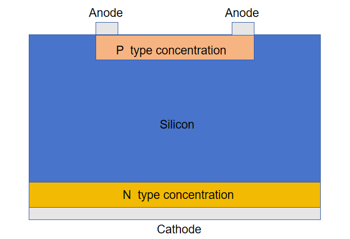
The basic structure of a commonly used PIN detector can be divided into three main regions: a P-type semiconductor (highly doped P-type semiconductor layer, hereinafter referred to as P layer), an intrinsic semiconductor (I layer), and an N-type semiconductor (highly doped N-type semiconductor layer, hereinafter referred to as N layer), which are stacked vertically (in the longitudinal direction).
As shown in Figure 1, the anode is located at the top of the device and typically receives the detected light signal from the anode aperture region. The anode is in direct contact with the P-layer, which has a higher doping concentration, and this region contains a large number of holes, which are the primary charge carriers. The intrinsic layer (I layer) is located between the P layer and the N layer; this region is intrinsic silicon (undoped region), which provides the photodetector's sensitivity to light. When light signals pass through this region, they excite electron-hole pairs, making it the core region for photoconversion. The cathode is located at the bottom of the device and is connected to the N-layer. This region contains a large number of free electrons, which are the primary charge carriers.
2.2. Principle of PIN detector
In a PIN detector, the reverse bias condition refers to the voltage applied between the P-type region and the N-type region, where the P-type region acts as the anode but is connected to the negative terminal of the external circuit, while the N-type region acts as the cathode but is connected to the positive terminal. Under this reverse bias, the direction of the applied electric field is the same as the direction of the built-in electric field within the semiconductor, both flowing from the N-type region to the P-type region. The energy bands in the P-type and N-type regions are bent as the electric field satisfies the relationship with the energy bands [4]:
The electric field in semiconductors (
Here,
Quantum efficiency is the ratio of the number of photogenerated carriers to the incident light [5]. Light-excited carriers drift toward their respective electrodes under the influence of an electric field. Under reverse bias, electrons and holes are accelerated, with electrons flowing toward the n-type region and holes flowing toward the p-type region, and are collected at the n-type and p-type electrodes, respectively. The collection process depends on the combined effects of drift and diffusion, and the finally collected electrons and holes form a current signal, which is the output signal of the PIN photodetector. The output current of the photodetector is directly proportional to the intensity of the incident light [6]. Therefore, the intensity of the incident light can be determined from the hole signal received at the anode. The greater the hole signal received at the anode, the greater the photocurrent, the more electron-hole pairs are stimulated, and the greater the intensity of the incident light. The principle of PIN detector is shown in Figure 2.
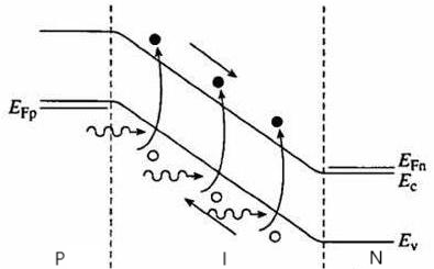
Figure 2: Principle of PIN detector
3. PIN simulation and characteristic analysis
3.1. Structure and simulation in dark state
This experiment was performed using Silvaco software. The PIN model structure was generated and environmental conditions were modified by writing code in Deckbuild to obtain Tonyplot images under different conditions for analyzing device characteristics. Figure 3 shows the PIN device plots. Subsequent changes in the simulation environmental parameters were based on changes in this model.
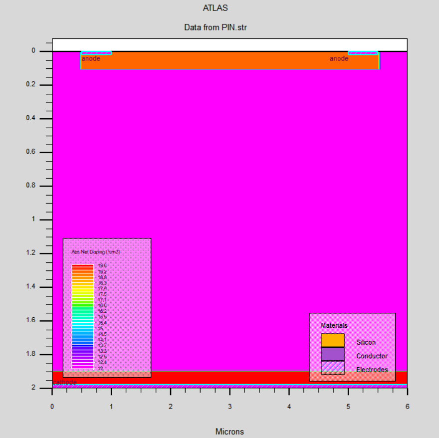
First, the silicon material region is defined, which is the entire device with a size of 6 μm in the x-direction and 2 μm in the y-direction. Within this region, uniform doping is applied to form the p-type, n-type and I-type regions of the PIN structure. The two anodes are located at 0.5 μm and 5 μm along the x-axis, with a width of 0.5 μm and a depth of 0.02 μm; the cathode depth is the same as the anode, but spans the entire device structure and is located at the bottom of the device. The p-type doping region is from 0.5 ≤ x ≤ 5.5 μm and 0 ≤ y ≤ 0.10 μm, with a doping concentration of
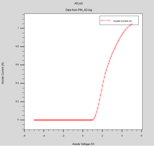
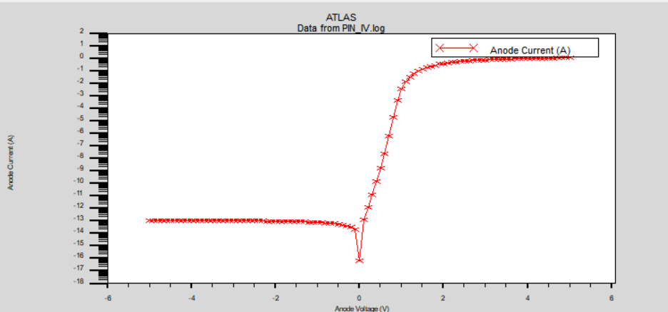
Set the anode voltage to rise from -5V to 0.2V. As shown in the I-V curve in Figure 4, in the dark state without illumination, when the PIN junction is reverse-biased, electrons and holes are attracted by the potential difference, resulting in a large depletion region and a high potential barrier. At this point, electrons and holes find it difficult to cross the PIN junction, resulting in high resistance and very low current. This indicates that the device generates almost no current in the dark state, with minimal current variation, consistent with the typical reverse saturation current characteristic.
As the reverse voltage gradually increases until it becomes positive, the current begins to gradually increase. Although the current variation is not particularly significant in this range, it gradually exhibits a more pronounced growth trend, especially as the voltage approaches or exceeds the threshold voltage (approximately 1.2V in this figure). Due to the increased injection and recombination of carriers in the PIN region, the device current exhibits a significant exponential increase, resulting in a current jump, demonstrating the unidirectional conductivity of the device [7]. The current characteristics can be described by the following formula:
Where I is the anode current flowing through the PIN junction (positive when forward-biased, negative during reverse bias);
3.2. Current characteristics under illumination
Based on the previous introduction to the principle of PIN photodetectors, PIN can detect light sources by measuring the magnitude of the output signal. When light strikes a PIN photodetector, photons are absorbed by the semiconductor material, producing photoelectrons and photoholes. These photogenerated carriers are separated by an electric field [8]. The photogenerated carriers interact with the electric field created by the reverse bias, are accelerated, and flow out through the electrodes, creating a current in the detector. The hole signal is received at the anode. As the parameters of the light change, such as wavelength, the number of carriers generated also changes, resulting in changes in the received signal.
In this experiment, a voltage of 24 V was applied to the cathode, i.e., a reverse bias voltage of 24 V. As analyzed earlier, under reverse bias, the region where the reverse current is very small shows minimal current changes, close to zero. When using linear coordinates, it can be difficult to see these subtle current variations. Using logarithmic coordinates can amplify and highlight these subtle current changes. As shown in Figure 5, the dark state voltage-current characteristics (logarithmic coordinates) indicate that the dark current is approaching
In the Figure 6, as the light wavelength increases from 0.2 μm to 0.5 μm (visible and ultraviolet light bands), the cathode current gradually increases with increasing wavelength, showing an upward trend [9]. This trend indicates that within this wavelength range, both light intensity and photoconversion efficiency gradually increase. The current reaches its maximum value at approximately 0.5 μm, indicating that the detector exhibits the strongest response to green light within this wavelength range. This is because this wavelength range typically corresponds to the green light region within the visible light spectrum, where silicon materials exhibit the highest light absorption and photoconversion efficiency.
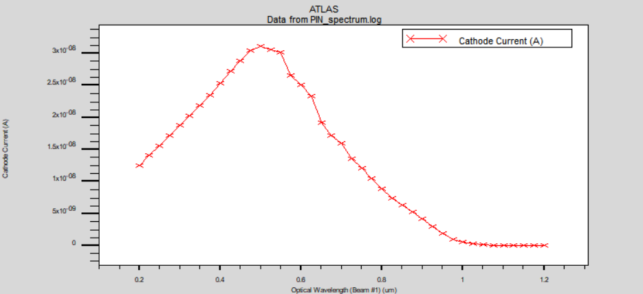
As the light intensity increases, the current may reach a saturation value and not increase significantly. From the peak, the current gradually decreases to near zero as the wavelength exceeds 0.5 μm. The PIN detector's ability to absorb light and convert it to electricity gradually decreases, with the rate of decrease becoming smaller and smaller until it levels off. At wavelengths near 1.2 μm (near infrared wavelength band), the cathode current reaches its minimum value and stabilizes, indicating that the device has entered the breakdown region. This is particularly pronounced at wavelengths above 1.2 μm. Silicon material exhibits extremely low absorption efficiency for long-wavelength light in this wavelength band, as photons beyond its effective light absorption range are unable to excite photogenerated carriers efficiently.
Overall, the PIN photodiode detector reaches its maximum response at 0.5 μm, indicating that the detector has the highest absorption and conversion efficiency for light at this wavelength. As the wavelength increases, the response of the photodetector gradually decreases, especially in the infrared region above 1.2 μm, where the response capability decreases significantly. In general, the absorption peak of silicon material typically occurs between 450 nm and 700 nm, which corresponds to the wavelength range where the cathode current peak is observed in the figure.
3.3. Electric field and potential distribution
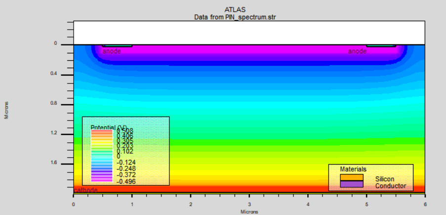
The details of the PIN detector under illumination conditions can be further analyzed by observing the potential and electric field distribution inside the detector. Since the reverse bias voltage supplied is 24 V, and the reverse bias voltage is applied from the cathode (high potential) to the anode (low potential), the potential gradually decreases in the direction from the cathode to the anode. As shown in the Figure 7, the highest potential at the cathode is approximately 0.5V, while the lowest potential near the anode is approximately -0.496V. As the distance from the cathode to the anode increases, the potential continues to decrease. The gradient direction of the potential change is from the cathode to the anode, which means that the direction of the electric field is also approximately from the cathode to the anode. This explains how light-induced charge carriers move toward the respective electrodes under the influence of the electric field. The hole signals are received at the anode. As shown in the figure, the potential at the anode is higher than the total potential of other regions in the P-type zone. This is because, under the influence of the electric field, the photo-excited carriers move and holes accumulate near the anode, causing the potential in this region to increase slightly and appear blue compared to the surrounding purple regions.
Under reverse bias, the electric field strength gradually changes throughout the semiconductor device. As shown in the Figure 8, the electric field strength is significant in the I-type region between the anode and cathode. Due to the extremely low carrier concentration in the I-type region, the electric field distribution in this region is relatively stable, and the electric field strength does not change because of the distribution or movement of the carriers. In other words, the electric field in the I-type region does not change due to charge accumulation or migration, and the electric field strength remains essentially constant [10]. Under illumination, the electric field acts on the photogenerated carriers in the I-type region, driving electrons toward the anode and holes toward the cathode. In the figure, especially in the P-type and N-type regions, where the carrier concentration is much higher than the intrinsic layer, the electric field strength is relatively high, which helps accelerate the movement of photo-excited carriers toward the electrodes and improves the response speed of the photodetector.
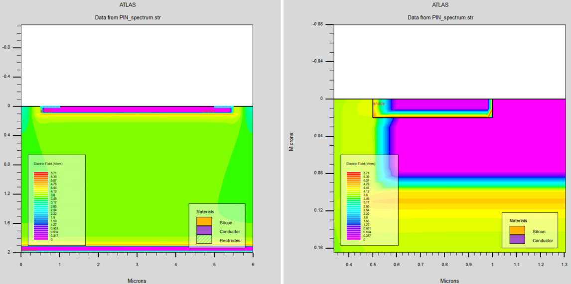
For the electric field in the electrode region, the electrode itself is a conductor with very high conductivity, so it quickly adjusts its internal potential to make the entire electrode surface an equipotential surface. Therefore, the potential in the electrode region remains essentially unchanged and the electric field is zero. However, between the electrode and the intrinsic semiconductor material, due to the accumulation of charges (e.g., between the anode and the semiconductor, where a large number of positively charged holes accumulate under the influence of a reverse bias voltage), the potential distribution in these regions is not continuous and smooth, but exhibits abrupt changes. Since E = -∇V, the electric field strength at the electrode-semiconductor interface also undergoes significant changes.
4. Conclusion
With the continuous advancement of optoelectronic detection methods, modern technology has placed new demands on the measurement range and response speed of PIN detectors. In this study, the operating characteristics of PIN photodetectors under different illumination conditions were systematically analyzed using Silvaco software, with special emphasis on their response performance in dark and illuminated states. First, the operating principle of PIN photodetectors under reverse bias was thoroughly investigated. Based on the Tonyplot images generated by the simulation analysis, the dark state characteristics of the device and the response regularity of current changes under different illumination wavelengths were revealed. Among them, the PIN detector exhibits the best response capability to green light at a wavelength of 0.5 μm and achieves the highest photoconversion efficiency. As the wavelength of light increases, the photoresponse of the device gradually weakens, especially in the near-infrared wavelength range, and shows a significant response decay trend. In addition, the distribution of potential and electric field further validated the drift mechanism of carriers under the influence of electric field in PIN photodetectors when excited by light, proving their efficient operation principle under different wavelength light sources.
This study provides a theoretical basis for the working mechanism of PIN photodetectors and offers practical data support for light source detection in different wavelength ranges. With ongoing advances in material science and fabrication processes, PIN photodetectors will continue to play an important role in high-sensitivity detection and high-speed data transmission applications.
References
[1]. Ramírez‐Jiménez F J. PIN diode detectors[C]//AIP Conference Proceedings. American Institute of Physics, 2008, 1026(1): 213-226.
[2]. Yu X, Marks T J, Facchetti A. Metal oxides for optoelectronic applications[J]. Nature materials, 2016, 15(4): 383-396.
[3]. Downs C, Vandervelde T E. Progress in infrared photodetectors since 2000[J]. Sensors, 2013, 13(4): 5054-5098.
[4]. Perlman S S, Feucht D L. PN heterojunctions[J]. Solid-State Electronics, 1964, 7(12): 911-923.
[5]. Song J, Wang O, Shen H, et al. Over 30% external quantum efficiency light‐emitting diodes by engineering quantum dot‐assisted energy level match for hole transport layer[J]. Advanced Functional Materials, 2019, 29(33): 1808377.
[6]. Barkelid M, Zwiller V. Photocurrent generation in semiconducting and metallic carbon nanotubes[J]. Nature Photonics, 2014, 8(1): 47-51.
[7]. Sah C T, Noyce R N, Shockley W. Carrier generation and recombination in pn junctions and pn junction characteristics[J]. Proceedings of the IRE, 2007, 45(9): 1228-1243.
[8]. Albery W J, Bartlett P N. The transport and kinetics of photogenerated carriers in colloidal semiconductor electrode particles[J]. Journal of the Electrochemical Society, 1984, 131(2): 315.
[9]. Konstantatos G, Clifford J, Levina L, et al. Sensitive solution-processed visible-wavelength photodetectors[J]. Nature photonics, 2007, 1(9): 531-534.
[10]. Lawrence E O, Linford L B. The Effect of Intense Electric Fields on the Photo-Electric Properties of Metals[J]. Physical Review, 1930, 36(3): 482.
Cite this article
Liu,X. (2025). Research and Characteristic Analysis of PIN Based on Simulation. Applied and Computational Engineering,169,25-34.
Data availability
The datasets used and/or analyzed during the current study will be available from the authors upon reasonable request.
Disclaimer/Publisher's Note
The statements, opinions and data contained in all publications are solely those of the individual author(s) and contributor(s) and not of EWA Publishing and/or the editor(s). EWA Publishing and/or the editor(s) disclaim responsibility for any injury to people or property resulting from any ideas, methods, instructions or products referred to in the content.
About volume
Volume title: Proceedings of CONF-MSS 2025 Symposium: Machine Vision System
© 2024 by the author(s). Licensee EWA Publishing, Oxford, UK. This article is an open access article distributed under the terms and
conditions of the Creative Commons Attribution (CC BY) license. Authors who
publish this series agree to the following terms:
1. Authors retain copyright and grant the series right of first publication with the work simultaneously licensed under a Creative Commons
Attribution License that allows others to share the work with an acknowledgment of the work's authorship and initial publication in this
series.
2. Authors are able to enter into separate, additional contractual arrangements for the non-exclusive distribution of the series's published
version of the work (e.g., post it to an institutional repository or publish it in a book), with an acknowledgment of its initial
publication in this series.
3. Authors are permitted and encouraged to post their work online (e.g., in institutional repositories or on their website) prior to and
during the submission process, as it can lead to productive exchanges, as well as earlier and greater citation of published work (See
Open access policy for details).
References
[1]. Ramírez‐Jiménez F J. PIN diode detectors[C]//AIP Conference Proceedings. American Institute of Physics, 2008, 1026(1): 213-226.
[2]. Yu X, Marks T J, Facchetti A. Metal oxides for optoelectronic applications[J]. Nature materials, 2016, 15(4): 383-396.
[3]. Downs C, Vandervelde T E. Progress in infrared photodetectors since 2000[J]. Sensors, 2013, 13(4): 5054-5098.
[4]. Perlman S S, Feucht D L. PN heterojunctions[J]. Solid-State Electronics, 1964, 7(12): 911-923.
[5]. Song J, Wang O, Shen H, et al. Over 30% external quantum efficiency light‐emitting diodes by engineering quantum dot‐assisted energy level match for hole transport layer[J]. Advanced Functional Materials, 2019, 29(33): 1808377.
[6]. Barkelid M, Zwiller V. Photocurrent generation in semiconducting and metallic carbon nanotubes[J]. Nature Photonics, 2014, 8(1): 47-51.
[7]. Sah C T, Noyce R N, Shockley W. Carrier generation and recombination in pn junctions and pn junction characteristics[J]. Proceedings of the IRE, 2007, 45(9): 1228-1243.
[8]. Albery W J, Bartlett P N. The transport and kinetics of photogenerated carriers in colloidal semiconductor electrode particles[J]. Journal of the Electrochemical Society, 1984, 131(2): 315.
[9]. Konstantatos G, Clifford J, Levina L, et al. Sensitive solution-processed visible-wavelength photodetectors[J]. Nature photonics, 2007, 1(9): 531-534.
[10]. Lawrence E O, Linford L B. The Effect of Intense Electric Fields on the Photo-Electric Properties of Metals[J]. Physical Review, 1930, 36(3): 482.