


1. Introduction
As the functionality and processing speed of digital chips continuously increase, their power consumption is also rising rapidly. This increase in power consumption leads to higher heat generation, especially in mobile consumer electronics where the demand for lower power consumption in digital chips is becoming more stringent. Excessive power consumption can significantly reduce the performance of the digital chip, making it unable to meet practical application requirements. Therefore, reducing power consumption without affecting performance has become a critical technology in chip development [1,2].
Currently, with the advancing technology of integrated circuits, the process size of semiconductor devices is continuously decreasing, and chip integration is increasing. This allows for more functional units to be integrated onto a single chip, leading to higher overall circuit power consumption. Additionally, the widespread use of battery-powered portable electronic products, such as PDAs, mobile phones, and laptops, has shortened battery life and exacerbated circuit thermal effects. Circuit power consumption has become a critical issue in circuit design, especially in VLSI design, which cannot be avoided.
As integrated circuit technology enters the deep sub-micron and ultra-deep sub-micron eras, power consumption has become another critical issue in the field of large-scale integrated circuit design, following performance and area. Therefore, research on low-power technology has taken on an extremely important role [3].
The mean time between failures (MTBF) of a product is related to its operating temperature, with MTBF = f(T), where f represents the average failure time period. Lower power consumption leads to a longer MTBF. Studies have shown that for every 10℃ increase in temperature compared to normal operating conditions, the failure rate of chips doubles, and the reliability of the entire circuit system significantly decreases. Thus, low-power design can effectively ensure that the circuit system avoids reliability degradation due to overheating.
The power consumption of digital integrated circuits consists of static power consumption caused by leakage current and dynamic power consumption caused by switching. Dynamic power consumption includes short-circuit power consumption, switching power consumption, and power consumption due to racing conditions caused by functional transitions. During the design process, designers often increase the static current to accelerate the speed of the unit circuit, which undoubtedly generates higher static power consumption. Additionally, the power consumption of digital integrated circuits is determined by the device’s operating voltage, operating frequency, load capacitance, and switching activity. Based on this, this article briefly analyzes the low-power optimization design of digital integrated circuits from the following aspects.
2. Power Consumption Composition of Digital Integrated Circuits
The power consumption of CMOS digital integrated circuits is composed of various factors and can be analyzed based on its types and components. Power consumption can be classified into dynamic power, static power, and surge power, with the proportion of each type varying according to application requirements and system architecture algorithms. The general classification of power consumption for CMOS digital integrated circuits is illustrated in figure 1.
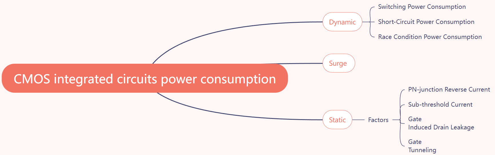
Figure 1: Composition of CMOS power consumption.
2.1. Dynamic power consumption
Dynamic power consumption can be further subdivided into switching power and short-circuit power based on its sources and characteristics [2], both of which have significant impacts on circuit design. Switching power, also known as toggle power, is primarily caused by the charging and discharging processes of capacitors. In digital circuits, especially CMOS (Complementary Metal-Oxide-Semiconductor) circuits, when the circuit state changes, the charge stored in the capacitors needs to be redistributed, leading to the generation of switching power [4]. Comparatively, short-circuit power, also referred to as internal power, arises from direct path currents that occur during circuit switching. This power consumption happens at the rising or falling edges of input signals when short-circuit paths may exist between low and high levels, resulting in instantaneous current flow and thus generating additional power consumption.
Although this article does not delve into the specific principles and formula derivations of dynamic power consumption in CMOS circuits, it is worth noting that the calculation formula for switching power and short-circuit power in CMOS inverters, as shown in Equation (1), indicates a direct proportional relationship between these two types of dynamic power and the switching activity factor (α), load capacitance (CL), the square of the operating voltage (V), and the operating frequency (f) . This implies that any changes in switching activity, operating frequency, or operating voltage during the design of CMOS circuits will directly affect the overall dynamic power consumption. Therefore, the magnitude of the load capacitance is determined by the standard cell library of the adopted process platform and the design constraints, requiring designers to find a balance among these factors.
Hence, the key to addressing dynamic power consumption in CMOS digital circuits lies in effectively managing the complex relationships between switching activity, operating frequency, operating voltage, and circuit functional modules [4]. By optimizing these parameters, designers can significantly reduce dynamic power consumption and improve energy efficiency of the circuits. Equation (1) not only provides a benchmark for power consumption calculation but also serves as a guiding tool in circuit design, assisting designers in making reasonable trade-offs and selections between functionality and power consumption.
P=α×CL× \( {V^{2}} \) ×f (1)
2.2. Static power consumption
Static power consumption refers to the energy dissipated by a circuit in the absence of any signal transitions, primarily arising from leakage currents. Leakage power encompasses several types:
First, PN-junction Reverse Current occurs due to the current generated when a PN junction is reverse-biased. Generally, this current is negligible under normal operating conditions; however, its impact becomes increasingly significant as process technologies shrink.
Second, Sub-threshold Current manifests when the gate voltage of a transistor falls below the threshold voltage. In this state, although the transistor is considered to be OFF, a certain proportion of charge carriers can still traverse the channel, resulting in leakage current.
Additionally, Gate Induced Drain Leakage (GIDL) constitutes an important component of static power consumption. This phenomenon affects the current flowing to the drain under the influence of gate voltage. It becomes particularly significant in modern technologies, where the scaling down of gate dimensions amplifies this leakage current[5].
Lastly, Gate Tunneling is a leakage phenomenon caused by quantum tunneling effects, especially pronounced in the presence of extremely thin oxide layers. The impact of this leakage current cannot be overlooked.
The magnitude and characteristics of static current are typically determined by the standard cell library associated with the employed process platform. Different process technologies utilize various materials and structures during fabrication, resulting in discrepancies in static power consumption. Therefore, in order to reduce static power consumption, design engineers must possess an in-depth understanding of the process platform and select appropriate design strategies to optimize circuit performance and enhance energy efficiency. Effectively managing these leakage currents presents a significant challenge in modern electronic design, particularly in the context of striving for higher integration levels and lower power consumption[6]. Through comprehensive study and understanding of various leakage currents, designers can formulate more effective power reduction strategies to meet the demands of contemporary electronic devices.
2.3. Inrush power consumption
Inrush power consumption refers to the energy dissipation caused by inrush current when powering on or waking up a device. Inrush current typically denotes the maximum current flowing through components during the initial power-up or when recovering from a low-power state. During these moments, the capacitors within the device require instantaneous charging, resulting in a rapid increase in current. This phenomenon is often referred to as “starting current.”
In many designs, inrush power consumption is frequently overlooked; however, this oversight can lead to abnormal issues during the power-on or wake-up processes. For instance, devices may experience failures or restarts due to an inability to withstand the transient spike in current. Moreover, excessive inrush current can potentially damage power components, connectors, and printed circuit boards (PCBs). Therefore, a thorough understanding of inrush power consumption is crucial for ensuring the stability and reliability of devices.
Effective management and design strategies for inrush power consumption place particular emphasis on the load capacity of the Power Management Unit (PMU). The design of the PMU must be capable of handling the high loads encountered during startup to ensure timely and stable power delivery when powering on or waking up the device. Additionally, digital logic timing synthesis design is closely related to inrush power consumption. In timing design, it is necessary to consider the circuit’s state during startup and the power supply’s response time to avoid timing instability or collisions during current surges[7].
Thus, strategies for optimizing inrush power consumption must extend beyond focusing solely on the power supply design; a system-level approach is required to ensure that all components operate in harmony, preventing excessive power consumption at critical moments. Through careful circuit design, appropriate component selection, and optimizing the load capacity of the PMU, designers can effectively mitigate the risks associated with inrush power consumption, thereby safeguarding the stable operation of devices.
3. Methods for reducing power consumption
Reducing power consumption in digital integrated circuits is of significant importance. On one hand, lowering power consumption can extend the usage life of battery-powered devices and enhance user experience. On the other hand, reducing power consumption helps in lowering system heat generation, thereby improving overall stability and reliability. Additionally, low-power design can reduce thermal management needs, simplifying cooling solutions and system design while saving costs. Lastly, in the context of environmental protection and sustainable development, reducing energy consumption also contributes to lowering carbon emissions, promoting the development of green electronic products. This article primarily introduces several methods for reducing power consumption, as illustrated in Figure 2 below.
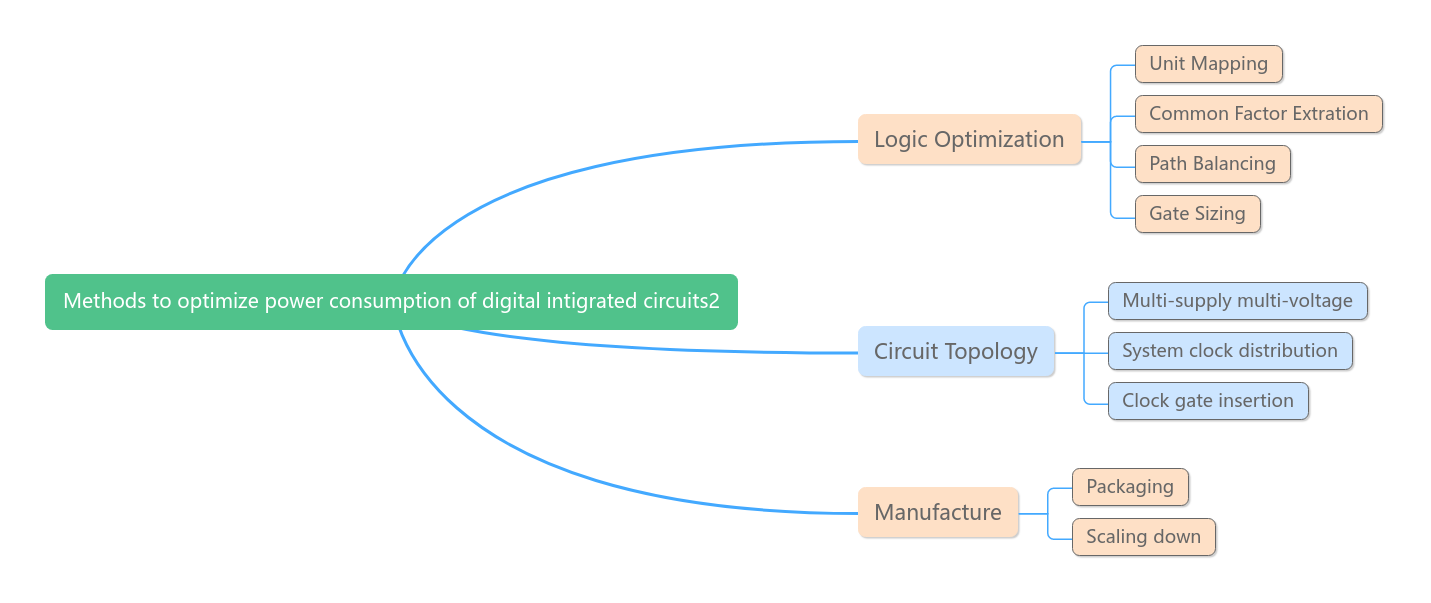
Figure 2: Approaches to optimize power consumption of digital circuits
3.1. Logic Optimization
Achieving low-power design in logic gate technology involves several aspects. Below are the primary strategies for reducing power consumption in digital integrated circuits.
3.1.1. Cell Mapping
At the gate-level description of a circuit, cell mapping is a crucial strategy for selecting logic gate units. Designers should utilize low-power logic gates provided in specific cell libraries. These gates are usually designed using advanced microarchitectures that can operate efficiently at lower voltages, significantly reducing power consumption. These low-power units not only optimize power usage but also ensure stability of the circuit during high-frequency operations. Additionally, by setting high-activity nodes inside the logic units, dynamic power consumption can be reduced while avoiding signal interference. Specific implementations include converting two-input logic gates into multi-input logic gates, which reduces the number of required logic layers, further lowering power consumption and increasing the speed and efficiency of data processing. This mapping method makes the design more flexible, allowing precise adjustments for different functional module requirements.
3.1.2. Common Factor Extraction
Common factor extraction is an important circuit simplification method that effectively reduces the operational cost and power consumption of the circuit. During the circuit design phase, a detailed analysis of the activity of each signal is required to identify frequently changing signals and low-activity signals. Designers can employ common factor extraction techniques to identify common parts among multiple signals and combine these common logic parts [8]. This not only reduces the number of logic gates required in the circuit but also simplifies interconnections and wiring, thereby reducing signal propagation delays and increasing power consumption. By optimizing signal transmission paths, the circuit can become more efficient, fully utilizing resources to achieve the dual goals of reducing power consumption and enhancing performance.
3.1.3. Path Balancing
Path balancing is a delay optimization technique aimed at ensuring that different input signals reach the same device input terminals at the same time. This design strategy can effectively reduce the additional switching phenomena caused by signal transmission delays, thereby lowering power consumption and improving circuit reliability. By adjusting path lengths or optimizing input signal wiring, designers can ensure that input signals arrive simultaneously, avoiding additional power consumption due to signal asynchrony. Furthermore, balancing path delays can also reduce timing issues in the circuit, improving the overall system performance. Combining path balancing with dynamic and static voltage adjustment strategies can further enhance the effectiveness of this technique, achieving significant reductions in power consumption.
3.1.4. Timing Adjustment
Timing adjustment is a flexible design strategy primarily achieved by repositioning registers within the circuit or adding new registers to optimize the time intervals for signal processing. This method can either extend the time interval for logic gate transitions or shorten the longest delay on the circuit, thereby effectively reducing power consumption generated during signal transitions. By optimizing the pipeline design, signal transmission between various logic gates becomes more coordinated, reducing multiple transitions at the input ports and enhancing information transmission efficiency. The optimized timing design not only reduces overall power consumption but also maintains zero error rates under high system loads, ensuring circuit stability under high-performance operating conditions [9]. Designers need to comprehensively consider circuit functional requirements and power consumption goals while conducting reasonable timing adjustments under the timing constraints [10].
3.1.5. Gate Size Optimization
Gate size optimization is a crucial aspect of power management, with the core idea being to reduce power consumption by intelligently adjusting the size of logic gates. Under conditions where circuit performance is not significantly impacted, appropriately reducing the size of logic gates on non-critical paths can significantly lower power consumption. For example, logic gates on non-critical paths can be designed to be smaller to reduce power consumption, while gates on critical paths should maintain an appropriate size to ensure the circuit’s response speed and stability. Additionally, for local circuits with large load capacitances, designers can choose larger units to optimize performance and use smaller units in later stages of the circuit to achieve overall power reduction. Common methods for gate size optimization include:
Linear Programming Method: Designers first linearize the timing constraints based on paths and then solve linear equations to obtain the optimal solution, primarily aiming to find the best combination of logic gate sizes.
Discrete Variation Optimization Method: Under time constraint conditions, optimization is carried out by gradually increasing the size of gates on critical paths until the constraints are met and activity is minimized. Additionally, under the premise of ensuring time constraints, the size of some gates can be appropriately reduced to achieve further power reduction.
Through these measures, designers can effectively implement low-power design in logic circuits. These strategies not only optimize circuit performance but also provide strong support for energy efficiency standards in modern electronic devices.
3.2. Circuit Structure Optimization
To reduce dynamic power consumption in chips, the most effective approach is to lower the operating voltage. This is because dynamic power consumption has a square relationship with the operating voltage, meaning that even a small reduction in voltage can significantly decrease power consumption. This section will introduce several major low-power voltage design techniques related to voltage.
3.2.1. Multi-Voltage Technology
Multi-voltage technology is an effective method for complex chips. Modern digital chips typically consist of multiple functional modules, each with different voltage requirements. Some modules, such as processor units, require higher operating voltages to ensure normal operation and high-frequency computing; other modules, like register units or memory units, only need lower voltages to perform basic functions [7]. Additionally, certain modules, such as control logic or counters, often operate at a stable medium voltage level.
By dividing different parts and modules of the chip into voltage regions according to their operating needs, demand-based power supply can be achieved. This is the core idea of multi-voltage technology. Each functional module can select the lowest power supply voltage that meets its performance requirements, thereby ensuring circuit performance while minimizing the dynamic power consumption of the entire chip. This design not only improves energy efficiency but also reduces chip heating and extends its lifespan.
3.2.2. Automatic Voltage Scaling Technology
Automatic voltage scaling technology further optimizes power management by designing a power management control unit in digital chips. This control unit monitors and controls the operating status of various modules in the chip. When the chip is in operation, the control unit automatically turns on the power for all modules and units related to the function to ensure the chip’s normal operation [8]. However, when the chip enters standby mode, the control unit automatically turns off the power for modules that do not need to work or lowers their operating voltage [9]. This process not only ensures the chip’s basic functions but also effectively reduces power consumption, achieving energy-saving goals.
When power supply modules no longer need to work, the control unit switches to a lower voltage to maintain the module in standby mode. This ensures that the module remains responsive without high-power processing. When these modules need to resume work, the control unit quickly wakes them up via the always-on power domain, ensuring they quickly enter operation mode. This flexible power management design ensures quick response from working modules while effectively reducing unnecessary energy consumption.
Moreover, register and memory modules in digital chips usually need to preserve their data after the system shuts down, so it can be used upon the next system power-up. When the system is off, registers and memories are no longer in operation and do not perform data read/write, so they do not require high operating voltages. At this time, the control unit can automatically lower the operating voltage to ensure that only enough power is input to maintain data storage, ensuring the system can effectively and quickly restart, immediately returning to the state before shutdown.
Through these low-power voltage design techniques, we can significantly reduce chip power consumption, enhance overall system performance and reliability, and drive modern electronic devices towards higher energy efficiency and performance standards.
In addition, dynamic power consumption has a direct proportional relationship with clock operating frequency. Therefore, by designing the clock reasonably, low-power goals can be effectively achieved. In integrated circuit design, chips often have conflicting clock demands: high clock frequency is needed for performance to enhance computing speed and processing capability, while low-frequency operation can effectively reduce power consumption. To meet performance requirements while minimizing power consumption, we can also consider clock gating technology.
Clock gating technology is an effective method to reduce power consumption by controlling the on/off state of the clock signal to reduce unnecessary energy consumption. Specifically, during certain periods when a module is idle or not working, its clock signal can be turned off. The core idea of this technology is “if not used, turn off,” reducing unnecessary clock signal transitions and lowering dynamic power consumption caused by the clock. In digital integrated circuit design, clock signal transitions are relatively frequent, typically accounting for about 20% of the entire chip’s power consumption. Traditional design methods usually keep the clock signal always active (always on) to ensure the chip can quickly respond at any time, but this also leads to significant power loss. Clock gating technology introduces a control signal into the design, which can gate the clock signal of unused modules based on actual needs, effectively reducing strategic point transitions and overall power consumption.
Figure 3 is a schematic diagram of a single clock gating design method, showing how the clock signal is managed through gating logic and how the control signal drives the activation and shutdown of modules.
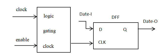
Figure 3: The design method of a single gated clock
3.3. Process Optimization
In the design of digital integrated circuits (ICs), achieving low-power design at the process level holds significant importance. This process primarily encompasses two core aspects: packaging technology and scaling technology. This article provides an in-depth exploration of these two technologies.
3.3.1. Scaling Technology
Scaling technology represents an effective method for reducing power consumption by increasing integration density. The integration density of a system is inversely proportional to the capacitance of devices and the communication volume between chips, indicating that higher integration density significantly reduces the required electrical energy while achieving the same functionality. Specifically, enhancing integration density can be achieved through several aspects:
Reduction of Device Quantity and Size: With technological advancements, the size of semiconductor devices has gradually decreased, allowing for the integration of more functional modules on a chip. For instance, adopting advanced transistor technologies (such as FinFET and Schmitt Trigger) can effectively enhance transistor switching logic while reducing power consumption. Increased integration density not only reduces the number of devices required in the circuit but also simplifies the wiring complexity needed to connect these devices. Multi-Layer Metal
Wiring Technology: As the process evolves, adopting a multi-layer metal wiring architecture has become an emerging trend. Using upper-layer metals for global interconnections not only reduces interconnect capacitance but also enhances signal transmission speed and stability. Multi-layered design allows for shorter interconnect paths, thus reducing signal delay, which is particularly important for high-speed operations. Additionally, the increase in metal layers enables more robust distribution of power and ground lines, improving power distribution and reducing signal-to-noise ratio.
Voltage Scaling: Under the premise of relatively stable device performance, moderately reducing the supply voltage is an effective strategy for reducing dynamic power consumption. The square relationship between dynamic power consumption and voltage indicates that a small reduction in supply voltage can achieve significant power reduction. For example, operating circuits at minimum working frequencies below a certain critical voltage can significantly extend the device’s operating time, especially crucial for mobile devices.
3.3.2. Packaging Technology
Within the entire circuit system, input/output (I/O) power consumption typically accounts for a significant portion of the overall system power, ranging from 25% to 50%. Therefore, when designing multi-chip systems, reducing I/O power consumption becomes a primary task. This can be achieved by reducing the capacitance of the I/O interface, such as reducing I/O capacitance: I/O capacitance directly impacts energy consumption during signal transitions. Adopting more efficient I/O interface designs and materials can effectively lower capacitance values. For example, using low-capacitance connectors and high-performance signal transmission lines can reduce power consumption due to capacitance while ensuring signal quality.
Signal integrity management can effectively optimize layout and wiring design to reduce the impact of parasitic capacitance and resistance on signal integrity. Techniques such as differential signal transmission can reduce power consumption and enhance immunity to interference, further improving I/O performance. Choosing appropriate packaging technology is also crucial. Multi-Chip Module (MCM) packaging is a packaging solution that significantly reduces power consumption generated by chip communication. MCM integrates multiple chips into a single package, significantly reducing the connection length between chips and thus lowering the inductance and capacitance of the lines, effectively reducing power consumption due to I/O.
When adopting MCM packaging technology, designers can also consider optimal interlayer interconnect layout, such as using micro-sized solder balls or adopting advanced packaging technologies like Chip Scale Package (CSP) and System in Package (SiP), which further enhance chip integration and overall performance.
Considering the future development, when implementing low-power design, multiple factors need to be taken into account, including the working environment of the circuit, practical application demands, and long-term reliability. For example, applications such as portable terminal devices require special attention to energy consumption to extend battery life, while in large data centers, reducing power consumption helps reduce operating costs and supports green environmental policies.
Looking ahead, with the development of emerging technologies such as the Internet of Things (IoT), Artificial Intelligence (AI), and 5G, the demand for low-power design will become increasingly urgent. Under the context of talent cultivation and new technology research and development, designers should continuously explore and research new processes and packaging technologies to address the growing challenges of power consumption and drive the entire industry towards higher energy efficiency standards.
In summary, implementing low-power design at the process level means effectively utilizing modern process and packaging technologies to achieve energy efficiency optimization in digital integrated circuits by enhancing integration density, reducing voltage, and decreasing I/O power consumption. These measures not only enhance the overall performance of the circuit but also provide strong support for the energy efficiency standards of the next generation of electronic devices.
4. Conclusion
This paper outlines the power consumption composition of CMOS digital integrated circuits and summarizes the currently mainstream power optimization methods from three aspects: logical gate optimization, circuit structure optimization, and manufacturing process improvement. It provides a comprehensive overview of digital integrated circuit optimization.
References
[1]. Shen, C. (2011). Research on key technologies of super dynamic voltage regulation for low-power SoC chips [D]. Southeast University, Jiangsu, China.
[2]. Rabaey, J. (2009). Low Power Design Essentials. Springer Berlin.
[3]. Aradhya, H. V. R., Kumar, B. V. P., & Muralidhara, K. N. (2012). Design of control unit for low power AU using reversible logic. Procedia Engineering, 30(9), 631-638.
[4]. Yang, B., Fan, Y. Y., Shi, Y. W., Guo, T., & Zhang, X. Q. (2018). Research on low-power voltage clock design for digital chips. Integrated Circuit Applications, 35(08), 17-19.
[5]. Srivastava, A. (2007). Statistical analysis and optimization for VLSI: Timing and power. Beijing: Science Press, 133-135.
[6]. Keating, M., Flynn, D., Aitken, R., Gibbons, A., & Shi, K. (2007). Low Power Methodology Manual for System on-Chip Design. Springer. Retrieved from http://www.synopsys.com/lpmm.
[7]. Chadha, R., & Bhasker, J. (2013). An ASIC low power primer-analysis. Techniques and Specification. Springer.
[8]. Veendrick, H., & Zhou, R. D. (2011). Nano CMOS integrated circuits: From basic principles to dedicated chip implementation. Beijing: Electronic Industry Press.
[9]. Sun, T. (2013). Low power design of mobile phone baseband chip [D]. Xidian University.
[10]. Rabaey, J. (2009). Low Power Design Essentials. Springer Berlin.
Cite this article
Yang,A. (2025). Low-Power Optimization Design Strategies for CMOS Digital Integrated Circuits. Applied and Computational Engineering,128,98-107.
Data availability
The datasets used and/or analyzed during the current study will be available from the authors upon reasonable request.
Disclaimer/Publisher's Note
The statements, opinions and data contained in all publications are solely those of the individual author(s) and contributor(s) and not of EWA Publishing and/or the editor(s). EWA Publishing and/or the editor(s) disclaim responsibility for any injury to people or property resulting from any ideas, methods, instructions or products referred to in the content.
About volume
Volume title: Proceedings of the 5th International Conference on Materials Chemistry and Environmental Engineering
© 2024 by the author(s). Licensee EWA Publishing, Oxford, UK. This article is an open access article distributed under the terms and
conditions of the Creative Commons Attribution (CC BY) license. Authors who
publish this series agree to the following terms:
1. Authors retain copyright and grant the series right of first publication with the work simultaneously licensed under a Creative Commons
Attribution License that allows others to share the work with an acknowledgment of the work's authorship and initial publication in this
series.
2. Authors are able to enter into separate, additional contractual arrangements for the non-exclusive distribution of the series's published
version of the work (e.g., post it to an institutional repository or publish it in a book), with an acknowledgment of its initial
publication in this series.
3. Authors are permitted and encouraged to post their work online (e.g., in institutional repositories or on their website) prior to and
during the submission process, as it can lead to productive exchanges, as well as earlier and greater citation of published work (See
Open access policy for details).
References
[1]. Shen, C. (2011). Research on key technologies of super dynamic voltage regulation for low-power SoC chips [D]. Southeast University, Jiangsu, China.
[2]. Rabaey, J. (2009). Low Power Design Essentials. Springer Berlin.
[3]. Aradhya, H. V. R., Kumar, B. V. P., & Muralidhara, K. N. (2012). Design of control unit for low power AU using reversible logic. Procedia Engineering, 30(9), 631-638.
[4]. Yang, B., Fan, Y. Y., Shi, Y. W., Guo, T., & Zhang, X. Q. (2018). Research on low-power voltage clock design for digital chips. Integrated Circuit Applications, 35(08), 17-19.
[5]. Srivastava, A. (2007). Statistical analysis and optimization for VLSI: Timing and power. Beijing: Science Press, 133-135.
[6]. Keating, M., Flynn, D., Aitken, R., Gibbons, A., & Shi, K. (2007). Low Power Methodology Manual for System on-Chip Design. Springer. Retrieved from http://www.synopsys.com/lpmm.
[7]. Chadha, R., & Bhasker, J. (2013). An ASIC low power primer-analysis. Techniques and Specification. Springer.
[8]. Veendrick, H., & Zhou, R. D. (2011). Nano CMOS integrated circuits: From basic principles to dedicated chip implementation. Beijing: Electronic Industry Press.
[9]. Sun, T. (2013). Low power design of mobile phone baseband chip [D]. Xidian University.
[10]. Rabaey, J. (2009). Low Power Design Essentials. Springer Berlin.