


1. Introduction
In recent years, metal halide materials have attracted significant attention as scintillators due to their high energy conversion efficiency, tunable wavelength and response time, and low fabrication cost. They have become star materials in the field of optoelectronic semiconductors. X-ray scintillation imaging is a key technology in medical diagnostics, industry, and security inspection. Indirect X-ray detection using scintillators converts high-energy X-ray radiation into low-energy ultraviolet/visible photons, which can be detected by conventional photodetectors to obtain digitized X-ray images [1, 2]. Scintillator-based X-ray imaging systems have become mainstream in the current market due to their relatively simple components and operational stability. However, traditional halide perovskite materials contain heavy metal lead (Pb) and toxic organic components, which severely limit their practical commercial application [3-5]. As a result, the synthesis and optical properties of lead-free halide perovskites have drawn increasing research interest. A new type of inorganic perovskite nanocrystal material, Cs₃Cu₂I₅, has emerged as a promising candidate due to its non-toxic nature and high stability, attracting considerable attention from researchers [6-8].
Colloidal scintillators composed of Cs₃Cu₂I₅ exhibit efficient radioluminescence and are promising for low-cost radiography and flexible X-ray imaging applications, and have received growing interest in recent years. However, there is still substantial room for improvement in the practical application of Cs₃Cu₂I₅ perovskite-based thin films:
First, the uniformity of transparent films with efficient radioluminescence is key to achieving high-resolution X-ray imaging. A major factor affecting film transparency is strong light scattering. Perovskite particles have a higher refractive index than typical organic and inorganic matrix materials, but how to efficiently extract light from scintillator particles within a polymer matrix with minimal loss remains a critical issue. Therefore, utilizing a semi-solid matrix with a refractive index close to that of the scintillator particles may offer a new approach to achieving higher light output.
Second, although Cs₃Cu₂I₅ has been extensively studied as a representative scintillator due to its excellent scintillation properties, its emission spectrum in the blue-light region aligns well only with the peak Quantum Efficiency (QE) of Photomultiplier Tubes (PMTs). In contrast, it is significantly mismatched with the peak QE of typical silicon-based photodetectors used in X-ray imaging, resulting in low scintillation photon collection efficiency. In follow-up studies, metal ion doping has demonstrated significant advantages in enhancing the light yield of scintillators, and spectral emission tuning can be achieved through doping strategies, structural adjustments, and compositional modulation. Rare-earth elements, in particular, have shown great potential in improving the optical performance of materials, effectively enhancing the luminescence efficiency and stability of scintillating films. However, despite their theoretical ability to deliver optimal luminescence performance, the practical application of rare-earth elements faces a series of challenges [9].
The high cost of rare-earth elements generally limits their feasibility for large-scale applications. Moreover, certain rare-earth elements exhibit a degree of toxicity, posing potential environmental and human health risks. This necessitates special attention to safety and environmental considerations during material production and usage. Therefore, there is an urgent need to develop a novel in-situ fabrication strategy that not only effectively reduces production costs but also improves the overall performance of Cs₃Cu₂I₅ nanocomposite scintillating films without compromising luminescence efficiency. Such a strategy would open broader prospects for future research and applications, driving the advancement of scintillation materials in a wide range of optoelectronic devices.
2. Preparation methods for polycrystals and scintillation screens
2.1. Preparation of Cs₃Cu₂I₅: Tb polycrystals
In this study, a scintillator polycrystal was synthesized using an in situ growth method, with the procedure detailed as follows:
To prepare the Cs₃Cu₂I₅: Tb polycrystal, copper (I) iodide (CuI, 98%, Aladdin), cesium iodide (CsI, 98%, Aladdin), and N, N-dimethylformamide (DMF, 99.9%, Aladdin) were used. First, TbCl₃•6H₂O was placed in a heating furnace and heated to 100 °C for 20 minutes to evaporate the water content, yielding a dried polycrystalline powder. Next, 1.5236 g (8 mmol) of CuI and 3.1178 g (12 mmol) of CsI were precisely weighed and added to a glass vial containing 5 mL of DMF, followed by 100 μL of hypophosphorous acid. The mixture was stirred at 60 °C on a magnetic hotplate for 30 minutes until fully dissolved into a transparent solution, forming the precursor solution. The Tb element was doped into the precursor solution at a specific molar ratio. Subsequently, the precursor solution was added dropwise into 5 mL of isopropanol as an anti-solvent. The transparent solution and isopropanol were mixed at a 1:5 ratio and stirred vigorously. The resulting mixture was centrifuged at 10,000 rpm for 5 minutes, leading to the precipitation of Cs₃Cu₂I₅: Tb polycrystals. The supernatant was discarded, and the precipitate was vacuum-dried at room temperature overnight. The resulting solid was ground thoroughly in an agate mortar to obtain the polycrystalline powder, as shown in Figure 1.
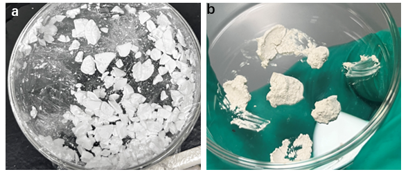
Figure 1. (a) Cs₃Cu₂I₅ polycrystalline powder and (b) Cs₃Cu₂I₅: Tb polycrystalline powder
2.2. Preparation of Cs₃Cu₂I₅: Tb scintillation film
The preparation process of Cs₃Cu₂I₅ thin films is illustrated in Figure 2. First, 2 g of Cs₃Cu₂I₅ polycrystalline powder (dried overnight in vacuum) was mixed with 0.6 g of carrier material and an appropriate amount of ethyl acetate. The mixture was stirred at 80 °C for 1 hour and collected as the precursor solution. This solution was then used to fabricate thin films by blade-coating onto a glass substrate that had been ultrasonically cleaned with acetone, ethanol, and deionized water for 30 minutes. The coated film was annealed on a hot plate at 75 °C. After the solvent fully evaporated, a Cs₃Cu₂I₅ scintillation film of a certain thickness was formed. Upon UV excitation, the fully crystallized film exhibited uniform blue luminescence and could be peeled off from the glass substrate. It is important to note that hotplate annealing can result in pinholes on the surface of the Cs₃Cu₂I₅ polycrystalline film after solvent evaporation, compromising film quality. Therefore, a constant-temperature oven annealing method was employed to allow faster and more uniform solvent evaporation, resulting in high-quality films. This improvement is attributed to the airflow in the oven, which promotes the rapid and even dispersion of DMF within the film, enabling simultaneous drying from the inside out and synchronous crystal growth of Cs₃Cu₂I₅ throughout the entire film.
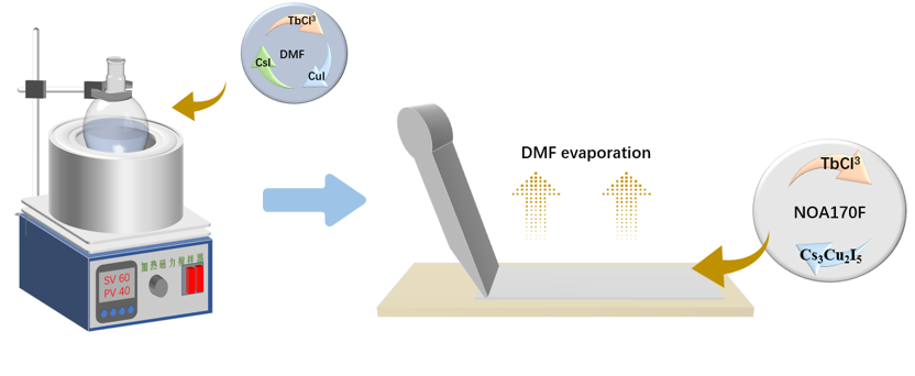
Figure 2. Preparation process of Cs₃Cu₂I₅: Tb film
When NOA170F was used as the carrier material, the preformed film was cured under nitrogen for 1 hour, as shown in Figure 3. Simultaneously, a 365 nm UV curing lamp with a power of 10 W was used for photopolymerization. After complete curing and solidification, the film could be peeled off.
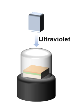
Figure 3. The carrier is cured as a NOA170F film
3. Phase analysis
3.1. Crystal structure of Cs₃Cu₂I₅: Tb
Due to the limited number of studies on Cu-based halide scintillators, there are no standard parameters such as PDF cards available for reference. Therefore, this study compares the obtained results with the information reported in relevant literature. While Cs₃Cu₂I₅ has been documented, no prior literature has reported the doping of Cs₃Cu₂I₅ with Tb. The experimental data presented here are provided for reference in future research.
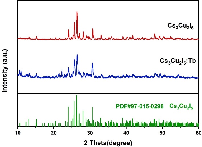
Figure 4. XRD patterns of (a) Cs₃Cu₂I₅ and (b) Cs₃Cu₂I₅: Tb
As shown in Figure 4, in the XRD pattern of Cs₃Cu₂I₅: Tb, the positions of the diffraction peaks correspond to the interplanar spacings of specific crystal planes. When compared with the standard XRD pattern of pure-phase Cs₃Cu₂I₅, a noticeable shift in the peak positions is observed, indicating the presence of Tb in Cs₃Cu₂I₅: Tb. This shift suggests that doping with Tb alters the lattice constants. The reason lies in the difference in ionic radii between Tb³⁺ and the substituted Cu⁺ ions, which leads to lattice distortion and an increase in the interplanar spacing. According to Bragg’s law, an increase in the interplanar spacing results in a decrease in the diffraction angle θ, which in turn causes the shift in the diffraction peak positions.
3.2. X-ray Photoelectron Spectroscopy (XPS)
The XPS spectra of both Cs₃Cu₂I₅ and Cs₃Cu₂I₅ doped with the rare earth element Tb are shown in Figure 5.
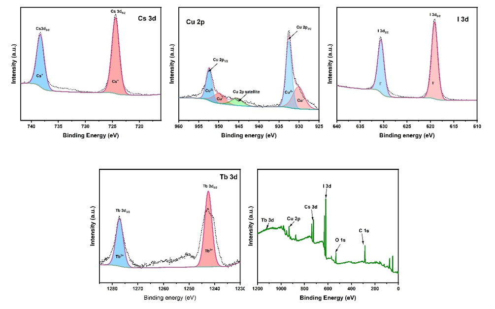
Figure 5. XPS spectra of Cs₃Cu₂I₅: Tb: (a) Cu 2p (b) I 3d (c) Cs 3d (d) Tb 3d (e) full spectrum
XPS analysis was used to further investigate the valence states of the elements in the material. As shown, the full spectra of both Cs₃Cu₂I₅ and Cs₃Cu₂I₅: Tb display characteristic peaks. High-resolution fitting reveals that in the Cu 2p spectrum, two distinct spin-orbit split peaks of copper’s 2p orbital are observed at 932.7 eV and 952.6 eV, with an energy separation of 19.9 eV. These correspond to Cu 2p₃/₂ and Cu 2p₁/₂, respectively, and match the binding energy of Cu⁺ in Cs₃Cu₂I₅. In the I 3d spectrum, the doublet peaks at 619.3 eV and 630.8 eV correspond to I 3d₅/₂ and I 3d₃/₂, with a separation of 11.5 eV. These values are consistent with the standard binding energies of iodide (I⁻). In the Cs 3d spectrum, the peaks at 724.6 eV and 738.6 eV represent Cs 3d₅/₂ and Cs 3d₃/₂, respectively, with a separation of 14 eV. These values correspond to Cs⁺, indicating that Cs exists in a single valence state. For the Tb spectrum in Cs₃Cu₂I₅: Tb, the peaks at 1230.5 eV and 1240.6 eV correspond to Tb 3d₃/₂ and Tb 3d₅/₂, respectively. The observed splitting of 10.1 eV is characteristic of Tb³⁺, and the peak positions align well with known values for Tb³⁺. Tb³⁺ has a higher positive charge than Tb²⁺, resulting in greater charge density and stronger attraction to surrounding electrons. This leads to higher binding energies for core electrons. As higher binding energy correlates with a shift of XPS peaks toward higher energy values, the absence of any noticeable shift toward lower binding energies suggests that Tb predominantly exists in the trivalent state, with no evidence of metallic or other valence states. Since XPS is a surface-sensitive technique and surface oxidation is common, the Cu 2p spectrum was examined for any signs of Cu²⁺ peaks. None were found, indicating that Cu⁺ is relatively stable and not easily oxidized, further supporting the material’s chemical stability. The above analysis confirms the presence of Cs, Cu, I, and Tb in the material, with Tb acting as a dopant and existing in the trivalent state.
4. Fluorescence characterization
After confirming that the material possesses a high-purity single phase, the optical properties of the material were further investigated. The optical performance of Tb-doped Cs₃Cu₂I₅ polycrystalline materials was examined, and the optimal doping concentration was selected for the fabrication of scintillator screens. Cs₃Cu₂I₅: Tb (15%) was taken as a representative sample to analyze the self-trapped exciton emission behavior of this material.
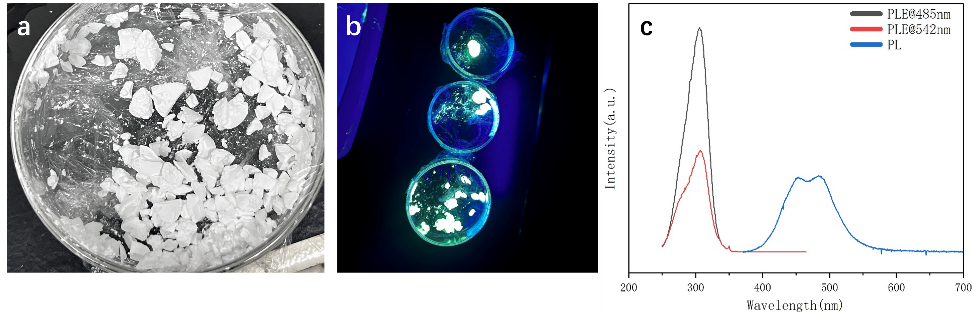
Figure 6. (a) Photographs of Cs₃Cu₂I₅: Tb polycrystalline under ambient light and ultraviolet light (254 nm); (b) Emission and excitation spectra
Emission spectra were first tested, as shown in Figure 6. The photographs reveal that Cs₃Cu₂I₅: Tb polycrystals appear pure white under ambient light, indicating negligible absorption in the visible range. Under UV excitation at 254 nm, the material emits a distinct blue-green light. Figure 6(c) presents the excitation spectrum of the Tb-doped Cs₃Cu₂I₅ polycrystalline material. The results show that Cs₃Cu₂I₅: Tb exhibits two prominent emission bands at 485 nm and 542 nm. The PL emission spectrum spans the entire visible range, with a strong and broad emission peak between 450–550 nm, indicating robust luminescence in this band and corresponding to the observed blue-green emission. The emission at 485 nm is similar to that of undoped Cs₃Cu₂I₅, which is attributed to self-trapped exciton luminescence, while the strongest characteristic emission peak at 542 nm corresponds to the ⁵D₄ → ⁷F₅ transition, a hallmark of Tb³⁺.
Using a dual-channel photoluminescence excitation spectrum analysis system, the energy level transition mechanisms of the emission bands at 485 nm (blue-green light) and 542 nm (yellow-green light) were studied in detail. As shown in the figure, both emission channels exhibit a broadened excitation band centered at 310 ± 2 nm, with highly consistent spectral profiles in the 295–325 nm range. This suggests that both emissions share a common matrix-activator charge transfer excitation pathway.
Through Jablonski diagram analysis, the corresponding Stokes shifts were calculated as Δλ_S (485) = 175 nm (ΔE = 1.72 eV) and Δλ_S(542) = 232 nm (ΔE = 2.01 eV), significantly exceeding those of typical inorganic scintillators. According to the Beer-Lambert law, the self-absorption coefficient α_self can be reduced to the order of 10⁻³ cm⁻¹, approximately two orders of magnitude lower than that of conventional scintillators. These findings provide critical evidence for subsequent analysis of potential energy transfer pathways and excitation relaxation mechanisms in Cs₃Cu₂I₅: Tb.
4.1. Fluorescence spectra of Cs₃Cu₂I₅: Tb
As shown in Figure 7, the PL spectra of Cs₃Cu₂I₅: Tb polycrystals with different doping concentrations under 254 nm UV excitation reveal that in the absence of Tb doping, the main emission peak appears between 445 nm and 540 nm, with the strongest emission at 445 nm, characteristic of the self-trapped exciton emission of pure-phase Cs₃Cu₂I₅. Upon Tb doping, as the concentration increases from 1% to 20%, the luminescence intensity increases significantly, indicating an energy transfer mechanism within the Tb-doped Cs₃Cu₂I₅ system. The excitation energy is gradually transferred to Tb³⁺ ions, and the strongest emission peak shifts to around 500 nm as doping increases, with bright green light observed. Additionally, a characteristic emission peak of Tb³⁺ ions emerges around 543 nm and intensifies with higher doping levels. This enhancement corresponds to the green emission associated with the ⁵D₄ → ⁷Fⱼ transition of Tb³⁺ ions. Generally, the ⁵D₄ → ⁷Fⱼ transition is a signature of Tb³⁺ ions. The luminescence of Tb³⁺ primarily originates from electronic transitions between its 4f–4f energy levels, especially the series of transitions from the excited state ⁵D₄ to the ground multiplet ⁷Fⱼ. Among these, the ⁵D₄ → ⁷F₅ transition corresponds to the strongest emission peak at 543 nm, which lies in the visible green region and finds broad application in display materials. This emission results from an electric dipole transition. Although 4f–4f transitions are forbidden in free ions, the symmetry breaking in crystals renders them partially allowed, resulting in strong luminescence. The spectral properties of this transition serve as a sensitive and stable optical probe for investigating energy transfer behavior in Tb³⁺-doped materials.
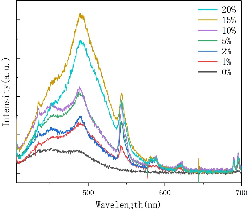
Figure 7. PL spectra of Cs₃Cu₂I₅: Tb polycrystalline at various concentrations under ultraviolet light (254 nm)
4.2. Fluorescence spectrum of Cs₃Cu₂I₅: Tb scintillation screen
As shown in Figure 8, the Photoluminescence (PL) spectra of Cs₃Cu₂I₅: Tb@NOA170F (15%) scintillator films with different thicknesses—220 μm, 310 μm, 330 μm, and 340 μm—are presented. By comparing the PL spectra of the films with varying thicknesses, it is evident that, since the scintillator polycrystalline powders are uniformly dispersed within the films, the loading of the scintillator powders varies with film thickness. Through repeated experiments with films of different thicknesses, it was found that the brightness of the scintillator films gradually increases with increasing thickness.
From the spectra, it can be observed that the PL emission intensity enhances progressively with the increase in film thickness. As the thickness increases from 220 μm to 340 μm, the emission intensity significantly improves. The PL intensity of the 220 μm film is relatively weak due to the lower absorption efficiency of the excitation light in thinner films. As a result, fewer Tb³⁺ ions are excited, leading to weaker emission. With increasing thickness, the penetration depth of the excitation light grows, allowing more Tb³⁺ ions to be excited and thus producing a stronger luminescent response. The emission intensity of the 340 μm film is nearly five times that of the 220 μm film. However, the emission intensity of the 340 μm film shows no significant increase compared to that of the 330 μm film, indicating that the enhancement trend is approaching saturation. This suggests that although thicker films can absorb more excitation light and activate more Tb³⁺ ions, the penetration of light becomes limited, especially in the inner layers of thicker films, where the absorption of excitation light diminishes. At this point, internal energy transfer and light scattering effects within the film slow the increase in emission intensity. Hence, further increasing film thickness may not effectively enhance luminescence performance, and oversizing the film can lead to saturation.
Regardless of whether the film is as thin as 220 μm or as thick as 340 μm, the emission peak remains within the same wavelength range, demonstrating stable luminescent characteristics. This emission peak stability indicates that the luminescence mechanism of the Tb³⁺-doped material is not significantly affected by variations in film thickness.
Moreover, although increasing the film thickness notably improves emission intensity, there are still several challenges and difficulties in the fabrication process of Cs₃Cu₂I₅ scintillator films doped with Tb and based on NOA170F. For instance, manufacturing thicker films is more difficult, and precise control over film thickness requires sophisticated techniques and depends heavily on manual blade-coating experience. Additionally, the uniformity and crystallinity of the material may be constrained by the growth conditions of thicker films. One of the key factors affecting image quality is the uniform dispersion of scintillator polycrystalline powders in the carrier. Although ethyl acetate is currently added to assist dispersion in industrial practice, its effectiveness remains limited. Finally, the film formation process for NOA170F-based scintillator films must be carried out in a vacuum or nitrogen-filled protective environment and cured with UV light at a wavelength of 365 nm. Therefore, there is still room for improvement in the mass industrial fabrication of such scintillator films. In actual production, it is necessary to consider the film thickness, emission intensity, and other physical properties comprehensively to achieve optimal scintillation performance.
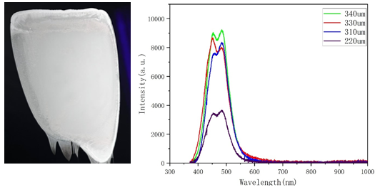
Figure 8. PL spectra of Cs₃Cu₂I₅: Tb@NOA170F (15%) scintillator films with different thicknesses and real image of the films
5. Imaging study of Cs₃Cu₂I₅: Tb scintillator screen
As demonstrated in the preceding sections, Cs₃Cu₂I₅ scintillator polycrystalline powder doped with rare earth element Tb exhibits characteristics such as high light yield, strong luminescence intensity, and a linear relationship with radiation energy, indicating its potential to serve as a high-performance scintillator. Consequently, this study developed a flexible Cs₃Cu₂I₅: Tb scintillator film featuring simple fabrication, high stability, excellent scintillation performance, and superior imaging resolution. In this section, a TPACI@NOA170F flexible scintillator film was fabricated using an insitu crystallization blade-coating method and evaluated using a laboratory-built X-ray imaging platform, demonstrating outstanding X-ray imaging performance. This work provides a promising approach for manufacturing high-resolution, flexible scintillator films.
Currently, no known industrial process uses NOA170F colloid as the host matrix for fabricating scintillator films. However, the preparation process resembles that of using PVDF as the film substrate. In 2016, Zhou et al. were the first to employ an in situ growth method to fabricate MAPbBr₃@PVDF composite films. The films were produced using a solvent casting–vacuum annealing method based on the non-solvent-induced phase separation mechanism. In the first stage, precursor molecules self-assemble: a 1.05:1 molar ratio of MABr/PbBr₂ and PVDF is co-dissolved in DMF, stirred magnetically at 800 rpm for four hours to obtain a stable colloidal solution with a zeta potential of +32 mV. This solution is then blade-coated onto an oxygen plasma-treated glass substrate to form a wet film.
The second stage involves controlling solvent evaporation kinetics: the wet film is transferred into a vacuum oven, where the DMF evaporation rate is modeled based on Fick’s second law. Drying is terminated when the residual solvent concentration falls below 0.1 wt%, resulting in a perovskite precursor framework encapsulated by β-phase PVDF. The third stage consists of in situ lattice reconstruction: topochemical conversion of MAPbBr₃ is performed in a nitrogen atmosphere annealing furnace. XRD analysis shows cooperative orientation growth between the cubic-phase perovskite and the PVDF (200) crystal plane.
In contrast, the fabrication of the Cs₃Cu₂I₅: Tb@NOA170F composite film differs in the second stage. After obtaining a uniform precursor coating, the film is cured under a nitrogen atmosphere for one hour using a UV curing lamp (wavelength 365 nm, power 10 W). Once fully solidified, the film can be peeled off.
Following the preparation of the Cs₃Cu₂I₅: Tb@NOA170F scintillator film with a doping concentration of 15%, X-ray imaging was conducted (see Figure 9). The spatial resolution of a scintillator is defined as the number of line pairs resolvable per millimeter. A line pair refers to a pair of equal-width bright and dark stripes or periodically spaced light-dark lines. Spatial resolution quantifies the film’s ability to resolve target details—the higher the resolution, the greater the detail discernibility.
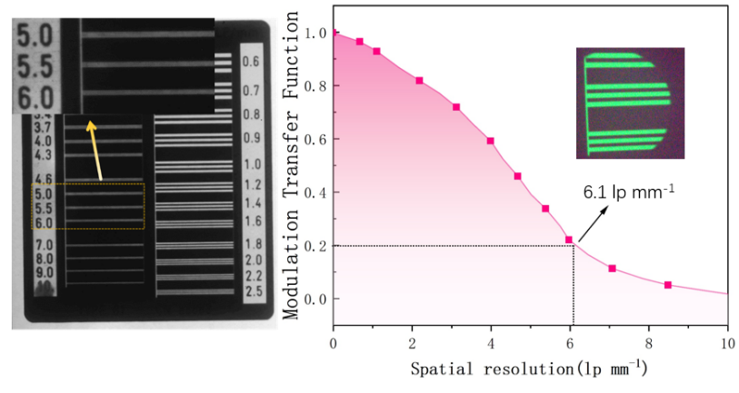
Figure 9. MTF curve of thin membrane
6. Conclusion
This study characterized the basic physical and luminescent properties of Cs₃Cu₂I₅ polycrystals doped with Tb and found that, compared to the pure-phase Cs₃Cu₂I₅, the doped material exhibits higher photoluminescence quantum yield and larger Stokes shift. Based on a doping concentration gradient, the optimal doping range for luminescence performance was determined, with a 15% doping level used as an example for STE luminescence analysis. Furthermore, the host matrix of the scintillator film was investigated and compared with commonly used matrices in the industry. The results show that NOA170F, as a film matrix, maximizes the luminescent performance of the scintillator film. The optimal doping ratio was established, and the resulting scintillator film exhibited excellent luminescent properties. It also demonstrated the capability for conformal X-ray imaging.
References
[1]. Liu, J., Shabbir, B., & Wang, C. (2019). Flexible, printable soft‐X‐ray detectors based on all‐inorganic perovskite quantum dots. Advanced Materials, 31(30), 1901644.
[2]. Sen, S., Tyagi, M., & Sharma, K. (2017). Organic-inorganic composite films based on Gd3Ga3Al2O12: Ce scintillator nanoparticles for X-ray imaging applications. ACS Applied Materials & Interfaces, 9(42), 37310-37320.
[3]. Lee, J. H., & Lee, J. W. (2022). Van der waals metal contacts for characterization and optoelectronic application of metal halide perovskite thin flms. ACS Energy Letters, 7, 3780-3787.
[4]. Qiao, L., Fang, W. H., & Prezhdo, O. V. (2022). Suppressing oxygen-induced deterioration of metal halide perovskites by alkaline earth metal doping: a quantum dynamics study. Journal of the American Chemical Society, 144, 5543-5551.
[5]. Zhao, F., Ren, A., &Li, P. (2022). Toward continuous-wave pumped metal halide perovskite lasers: strategies and challenges. ACS Nano, 16, 7116-7143.
[6]. Zhou, Y., Chen, J., &Bakr, O. M. (2021). Metal Halide Perovskites for X-ray Imaging Scintillators and Detectors. ACS Energy Letters, 6(2), 739-768.
[7]. Wu, H., Ge, Y., &Niu, G. (2021). Metal Halide Perovskites for X-Ray Detection and Imaging. Matter, 4(1), 144-163.
[8]. Jana, A., Cho, S., &Patil, S. A. (2022). Perovskite: Scintillators, Direct Detectors, and X-ray Imagers. Materials Today, 55, 110-136.
[9]. Dunlap-Shohl, W. A., Zhou, Y., Padture, N. P., & Mitzi, D. B. (2019). Chemical Reviews, 119, 3193.
Cite this article
Chen,H. (2025). Study on rare-earth element-doped copper halides. Advances in Engineering Innovation,16(6),35-42.
Data availability
The datasets used and/or analyzed during the current study will be available from the authors upon reasonable request.
Disclaimer/Publisher's Note
The statements, opinions and data contained in all publications are solely those of the individual author(s) and contributor(s) and not of EWA Publishing and/or the editor(s). EWA Publishing and/or the editor(s) disclaim responsibility for any injury to people or property resulting from any ideas, methods, instructions or products referred to in the content.
About volume
Journal:Advances in Engineering Innovation
© 2024 by the author(s). Licensee EWA Publishing, Oxford, UK. This article is an open access article distributed under the terms and
conditions of the Creative Commons Attribution (CC BY) license. Authors who
publish this series agree to the following terms:
1. Authors retain copyright and grant the series right of first publication with the work simultaneously licensed under a Creative Commons
Attribution License that allows others to share the work with an acknowledgment of the work's authorship and initial publication in this
series.
2. Authors are able to enter into separate, additional contractual arrangements for the non-exclusive distribution of the series's published
version of the work (e.g., post it to an institutional repository or publish it in a book), with an acknowledgment of its initial
publication in this series.
3. Authors are permitted and encouraged to post their work online (e.g., in institutional repositories or on their website) prior to and
during the submission process, as it can lead to productive exchanges, as well as earlier and greater citation of published work (See
Open access policy for details).
References
[1]. Liu, J., Shabbir, B., & Wang, C. (2019). Flexible, printable soft‐X‐ray detectors based on all‐inorganic perovskite quantum dots. Advanced Materials, 31(30), 1901644.
[2]. Sen, S., Tyagi, M., & Sharma, K. (2017). Organic-inorganic composite films based on Gd3Ga3Al2O12: Ce scintillator nanoparticles for X-ray imaging applications. ACS Applied Materials & Interfaces, 9(42), 37310-37320.
[3]. Lee, J. H., & Lee, J. W. (2022). Van der waals metal contacts for characterization and optoelectronic application of metal halide perovskite thin flms. ACS Energy Letters, 7, 3780-3787.
[4]. Qiao, L., Fang, W. H., & Prezhdo, O. V. (2022). Suppressing oxygen-induced deterioration of metal halide perovskites by alkaline earth metal doping: a quantum dynamics study. Journal of the American Chemical Society, 144, 5543-5551.
[5]. Zhao, F., Ren, A., &Li, P. (2022). Toward continuous-wave pumped metal halide perovskite lasers: strategies and challenges. ACS Nano, 16, 7116-7143.
[6]. Zhou, Y., Chen, J., &Bakr, O. M. (2021). Metal Halide Perovskites for X-ray Imaging Scintillators and Detectors. ACS Energy Letters, 6(2), 739-768.
[7]. Wu, H., Ge, Y., &Niu, G. (2021). Metal Halide Perovskites for X-Ray Detection and Imaging. Matter, 4(1), 144-163.
[8]. Jana, A., Cho, S., &Patil, S. A. (2022). Perovskite: Scintillators, Direct Detectors, and X-ray Imagers. Materials Today, 55, 110-136.
[9]. Dunlap-Shohl, W. A., Zhou, Y., Padture, N. P., & Mitzi, D. B. (2019). Chemical Reviews, 119, 3193.