


1. Introduction
Looking ahead to around 1960, Bell Labs and Fairchild Semiconductor successively invented silicon-based field-effect transistors and complementary metal oxide semiconductor technology, namely MOSFET and CMOS technology. After early exploration, the semiconductor integrated circuit industry followed the business rule of Moore’s Law, which states that the degree of silicon-based circuit integration will double every 18 to 24 months, and developed rapidly, ushering in a new era of silicon-based circuit development, and leading the information revolution, enabling the rapid development of the integrated circuit industry. However, since the 21st century, integrated circuits composed of silicon-based transistors have faced physical challenges [1]. The cost of scaling down silicon-based transistors has become increasingly high, the difficulty of scaling down has become increasingly greater, and the design of silicon-based semiconductors has become more complex. Although various emerging technologies have been invented to counteract the physical characteristics of silicon-based transistors, as we approach 2023, the cost of scaling down silicon-based transistors is becoming increasingly high, the speed is becoming slower, and the results obtained are becoming smaller, while the expenditure is seriously inadequate compared to the results obtained. At the same time, the physical process bottleneck of silicon-based integrated circuits is difficult to break through. The development speed of semiconductors, as the cornerstone of the integrated circuit industry and even the entire information industry, is gradually stagnating. While the industry is exploring further research directions for silicon-based semiconductors, it is also exploring more new materials. Among them, due to their excellent structural performance, carbon nanotubes have become a new type of semiconductor material that people attach great importance to, and people are also investing extensive attention and continuous research in carbon-based semiconductors.
This article will delve into silicon-based and carbon-based integrated circuits, explore the current research status and development direction of silicon-based and carbon-based semiconductors in the present era, compare the differences and advantages and disadvantages of the two materials in various performance aspects, summarize and generalize the current application scenarios of the two materials, and further explore the possible future application scenarios, looking forward to the development direction of the integrated circuit industry in the future.
2. Performance comparison between silicon-based integrated circuit and carbon-based integrated circuit
2.1. Silicon-based integrated circuit technical description
CMOS, as represented by silicon-based technology, has had high integration and low power consumption since its invention. Therefore, it is widely used in various modern electronic products. With the rapid development of integrated circuits, silicon-based technology has transitioned from micrometre to nanometre scale for large-scale integrated circuit manufacturing. The volume of field-effect transistors continues to decrease.
Currently, the latest manufacturing process has reached 3nm. However, the enhancement of circuit performance is progressively diminishing and nearing the physical limits attainable through silicon-based technology, while the gains in performance and efficiency achievable through advancements in the manufacturing process are becoming increasingly limited [2]. Furthermore, due to the different transistor structures, the performance differences of circuits under the same process with different structures gradually widen, placing higher demands on manufacturing processes.
2.2. Carbon-based integrated circuit research progress
Since its discovery in 1991, carbon nanotubes have been studied as a new type of material. As Moore’s Law gradually loses its effectiveness and silicon-based technology approaches its physical limit, people have discovered that carbon nanotubes have high-performance potential. Their intrinsic quantum capacity is relatively small, making them easy to gate-control, and their carrier screening length is short which helps to suppress the short channel effect of transistors. Experimental studies have shown that carbon nanotubes have high open state performance and can effectively inhibit leakage current, and reduce static power consumption, therefore, making them an attractive option as they balance high performance with low power. Thus, carbon nanotubes have high research and development potential as well as promising future application prospects.
As of now, there are mainly three types of carbon nanotube materials, namely, single-walled carbon nanotubes, carbon nanotube networks, and carbon nanotube parallel arrays. Among them, carbon nanotube arrays are the ideal material for carbon-based integrated circuit manufacturing. The dimensional confinement method proposed by the Peking University team is currently the theoretically densest and highest purity nanotube parallel array, which can basically meet the basic requirements of the carbon-based integrated circuits industry. CMOS manufactured under this material has a saturation current of 1.3 mA/µm, a peak transconductance of 0.9 mS/µm, and a steepness of 75 mV/dec at 1V operating voltage. The ring oscillator circuit speed can reach 8.06 GHz [9]. However, due to technological limitations, further research and development of carbon-based integrated circuit materials are required. The reliability and mass production optimization of the circuits still need to be further improved and studied, and various issues related to carbon-based integrated circuits need to be addressed. Moreover, there is currently a lack of standardized carbon nanotube materials and process specifications in the industry. The advantage of carbon nanotubes on integrated circuits is shown in figure 1 [2].
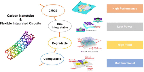
Figure 1. Advantage of carbon nanotube on integrated circuits [2].
2.3. Performance comparison and analysis
Currently, the core focus of research and development in the industry of Very Large Scale Integration (VLSI) is not only focused on reducing the size of CMOS circuits, improving circuit performance, and reducing power consumption, but also on reducing heat generation and unnecessary power consumption, improving circuit efficiency, and further reducing the size of peripherals (such as reducing the size of heat dissipation modules) required by the entire system. In recent years, various new transistor structures have emerged, but whether the carbon nanotube transistor structure mentioned in this paper has further application potential needs to consider whether it can address the main concerns of the industry. Experimental data shows that carbon nanotubes have high application potential.
According to relevant theories, simulations, and experiments, carbon nanotube transistors have a higher average carrier mean free path, higher low-field mobility, stronger high-field saturation velocity, and higher ballistic injection velocity. Compared to silicon-based transistors, they have a fourfold increase in high-field saturation velocity ( \( {4×10^{7}} \) cm/s) and more than a threefold increase in ballistic injection velocity ( \( {3×10^{7}} \) - \( {4×10^{7}} \) cm/s) [3-5]. The improvement of these performance parameters significantly enhances device performance and processing speed. Based on experimental results which been mentioned before, it has been demonstrated that carbon nanotube transistors with a gate length of 120 nm can achieve a current density of 1.18 mA/µm at a working voltage of 1 V, and the gate delay of the ring oscillator circuit can be reduced to 11.3 ps, surpassing the performance of silicon-based transistors of the same size. This study has proven the high research value of carbon nanotubes [6].
In summary, compared to CMOS, carbon nanotubes are a new type of material used to build CMOS, that combines high performance and low power consumption characteristics, and can further extend the effectiveness and meet the future requirements of Moore’s Law.
3. Analysis of Very Large Scale Integration (VLSI) applications
3.1. Current applications of silicon-based integrated circuits
In the past 60 years, the semiconductor integrated circuit with silicon as its core has rapidly promoted the development of the information revolution. Silicon-based circuits have undergone rapid iteration and have developed to their current state. Currently, silicon-based integrated circuits are common in electronic devices such as logic devices, storage devices, diodes, and transistors, and are mainly used in most consumer and commercial electronic devices such as mobile phones and computers. In recent years, they have become the cornerstone of Artificial Intelligence (AI) computing, 5G connectivity, Internet of Things (IoT), and other fields. Since the Bell Laboratory manufactured the first transistor in 1948, major companies have successively established themselves and begun to attack the integrated circuit industry [7]. The semiconductor process has gradually entered within 100nm from 10μm in 1971 to 14nm, 10nm, 7nm, 5nm, and the latest 3nm.
From the silicon-based technology been developed, and compared with other mainstream integrated circuit manufacturing solutions, it has lower process costs, higher integration, and can integrate the functions of signal processing and other digital modules. It has been widely used and researched in academia and industry. Taking the silicon-based RF millimetre-wave phase shifter as an example, due to the extremely crowded spectrum resources in the wireless communication industry, countries led by the United States have taken the lead in using millimetre-wave bands as a communication method for 5G communication. Although millimetre-waves currently face many challenges, silicon-based RF millimetre-wave phase shifters perform significantly better than traditional millimetre-wave solid-state phased array systems manufactured using compound semiconductor processes in terms of cost, integration, and production yield while having a smaller circuit size. Therefore, silicon-based RF millimetre-wave phase shifters have been widely used in emerging fields such as 5G communication. At the same time, as one of the core modules of the silicon-based phased array system, the silicon-based RF millimetre-wave phase shifter has also been continuously researched by a large number of scholars [8].
In the x86 processor field, chip companies led by Intel have gradually developed from the 4004 series processor with a 10μm process introduced in 1971, following Moore’s Law, to subsequent releases such as the 8086 series, Pentium series, Core series, Xeon series processors, etc. Starting in 2014, Intel released the first 14nm processor and suspended further research and development in chip processes. Instead, they continued to optimize the performance and process of the 14nm architecture, promote processor performance, and continue to maintain the ‘Number of transistors that can be accommodated on an integrated circuit will double every 18 to 24 months’ under the same standard process. However, it is obvious that the performance improvement and efficiency enhancement of both Intel and AMD in the field of processors are becoming less and less. Advanced integrated circuits require higher power consumption to achieve a performance improvement, and mobile PCs require stronger cooling performance to meet the higher cooling demand caused by high power consumption and low efficiency. The Development of Intel process technology is shown in figure 2 [9].
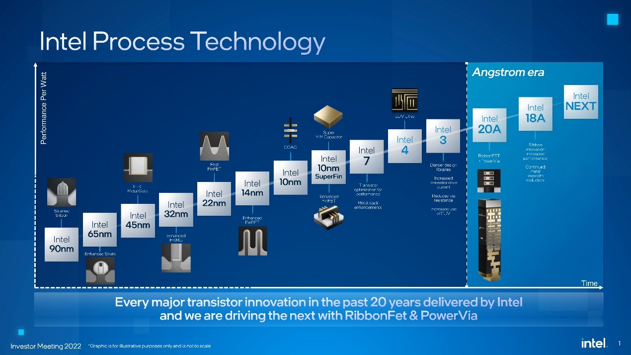
Figure 2. Development of Intel process technology [9].
3.2. Current Applications of Carbon-based Integrated Circuits
Although carbon-based electronic technology is not commonly seen in the consumer electronics industry, it has undergone long-term development. It not only has advantages in performance parameters and size but also has great application potential. It can not only replace most of the application scenarios of silicon-based integrated circuits but also show tremendous potential in some emerging industries.
In digital integrated circuits, carbon-based integrated circuits have excellent parameters due to the superior chemical properties of carbon nanotubes. As mentioned earlier, carbon-based integrated circuits have advantages such as high carrier mobility, high injection rate, and high strong-field saturation velocity compared to silicon-based integrated circuits. At the same time, the manufacturing process of carbon-based circuits is simpler than that of silicon-based circuits. These advantages enable carbon-based integrated circuits made of carbon nanotubes to better meet the requirements of future digital integrated circuits for circuit device performance and continue to align with the development of Moore’s Law. As the application direction with the highest technological value and commercial value in carbon-based electronic technology, the development of carbon-based integrated circuits in recent years mainly includes four aspects: the exploration of high-performance circuits, innovation of low-power devices, demonstration of complete digital logic functions, and research on large-scale integrated systems. In 2006, IBM constructed a CMOS five-stage oscillator on a carbon nanotube and achieved a maximum oscillation frequency of 52MHz, with a gate delay of only 1.9ns [10]. After research and development in the academic community, in 2020, the highest oscillation frequency of 8.06 GHz in a PMOS five-stage oscillator circuit with a gate length of 165 nm, and a gate delay of only 12.4 ps [11]. This experiment data surpasses the experimental data of commercially available silicon devices of the same size mentioned earlier, fully demonstrating the enormous application potential of carbon-based circuits in digital integrated circuits, and proving that the performance bottleneck of carbon-based circuits is not limited to this and its performance can be further explored and proven. At the same time, there is also greater optimization space for carbon based integrated circuits in terms of power consumption.
Currently, silicon-based circuits have physical bottlenecks in power consumption and process. In the past three years, Qualcomm’s mobile platform processors manufactured by Samsung Semiconductor have been known for their high power consumption. Taking Qualcomm’s Snapdragon 8 Generation 1 mobile platform processor launched in 2022 as an example, in experimental tests, the power consumption of Motorola mobile platform equipped with this processor even reached 11.10W, which is nearly doubled compared to iQOO mobile platform equipped with Qualcomm’s Snapdragon 870 processor launched in 2021, which had a power consumption of only 5.52W. Due to the significant increase in power consumption and the characteristics of mobile platforms, the motherboard generates excessive heat, ultimately seriously affecting performance [12]. The theoretical performance of mobile platforms equipped with Qualcomm’s Snapdragon 8 Generation 1 processor does not match its actual performance and even shows signs of regression compared with the last generation chip. Therefore, carbon nanotubes, as emerging materials for consumer and commercial integrated circuit products, have high research value.
4. The challenge facing the development of integrated circuits
Prior to achieving commercialization, the first hurdle to overcome is market restrictions. Currently, chip companies led by Intel are actively adopting silicon-based integrated circuits and hoping to further expand their performance to continue their development. Therefore, for carbon-based integrated circuits, new entrants lack consumer understanding and OEM manufacturers’ trust at the market level. At the same time, the failure mechanism of carbon-based integrated circuits is more complex and has a greater impact on the overall reliability of the device, especially compared to silicon-based integrated circuits with long-term development experience, presenting a certain deficiency. In addition, compared with typical design support such as EDA, automated design tools, and design toolkits in silicon-based integrated circuits, carbon-based integrated circuits lack these, and the industry needs a set of standards and professional tools to promote the development and commercialization of carbon-based integrated circuits [13].
Finally, regarding the standardization of carbon-based integrated circuits, the production and application of carbon nanotube materials are still in the laboratory stage, and the production methods and final application framework architecture are not unified. The industry requires a unified set of standards to develop production methods for carbon nanotubes, define reference ranges of specific parameter standards, and establish corresponding indicators to ensure that carbon-based integrated circuits made from carbon nanotubes can be mass-produced using strict semiconductor industry process standards. Only by completing all current challenges can carbon-based integrated circuits truly enter the commercialization stage of large-scale mass production with reliability and trust.
5. Conclusion
After more than 60 years of development, the integrated circuit industry has become an essential part of people’s daily lives, and the semiconductor industry is almost one of the fastest-growing industries. In less than 100 years, the silicon-based integrated circuit fabrication process has been developed to near the physical limit, while carbon-based integrated circuits based on carbon nanotubes have been developed for over 20 years and now have a certain application base. Various experimental data have proven that carbon nanotubes, as a highly potential and widely researched new semiconductor material, have research value in extending Moore’s Law, and they are ideal materials for replacing silicon semiconductors. They are also a cornerstone for the sustained development of the integrated circuit industry and the continued progress of the information revolution. Meanwhile, laboratory results have shown that integrated circuits made of carbon nanotubes can replace silicon-based integrated circuits and even exhibit performance data beyond that of silicon-based integrated circuits. This means that carbon-based integrated circuits have a high degree of commercial potential. In recent years, breakthroughs have been made in the preparation of carbon nanotubes in academia, and carbon-based integrated circuits have demonstrated advantages in multiple fields, whether it is the high-performance and low-power carbon-based integrated circuits or other efficient carbon-based circuit systems, all of which prove that the industrialization and commercialization of carbon-based integrated circuits are no longer impossible to achieve. Therefore, real success is still dependent on commercialization, and the challenges that need to be faced before industrialization include process standardization and the establishment of a professional software ecosystem. Carbon-based integrated circuits have obvious advantages, but further research and development of carbon-based semiconductors and the borrowing of successful experiences from silicon-based semiconductors, along with strong support from various companies, are needed to truly realize the industrialization and commercialization of carbon-based integrated circuits.
References
[1]. Zhichao Ye, Haiyan Jia, Zhangjun Huang, Chen Shen, Jinbao Long, Baoqi Shi... & Junqiu Liu. (2023). Foundry manufacturing of tight-confinement, dispersion-engineered, ultralow-loss silicon nitride photonic integrated circuits. Photonics Research (04),558-568.
[2]. Chao Xiang, Warren Jin & John E. Bowers. (2022). Silicon nitride passive and active photonic integrated circuits: trends and prospects. Photonics Research (06), 82-96.
[3]. Zhou Peigen, Chen Jixin, Tang Siyuan, Yu Jiayang, Wang Chen, Li Huanbo... & Hong Wei. (2022). Research on Silicon-Based Terahertz Communication Integrated Circuits. Chinese Journal of Electronics (03),516-533.
[4]. Xie Yunong & Zhang Zhiyong. (2021).Carbon nanotube-based CMOS transistors and integrated circuits. Science China Information Sciences (10).
[5]. Das Uttam Kumar & Hussain Muhammad M.. (2021).Benchmarking Silicon FinFET With the Carbon Nanotube and 2D-FETs for Advanced Node CMOS Logic Application. IEEE transactions on electron devices (7).
[6]. Swapnajit Chakravarty, Min Teng, Reza Safian & Leimeng Zhuang. (2021).Hybrid material integration in silicon photonic integrated circuits. Journal of Semiconductors (04),37-46.
[7]. Hu QingHao, Zhao WenSheng, Fu Kai, Wang DaWei & Wang Gaofeng. (2020). On the applicability of two‐bit carbon nanotube through‐silicon via for power distribution networks in 3‐D integrated circuits. IET Circuits, Devices & Systems (1).
[8]. P. V. Fontana, J. P. Decosterd & L. Wegmann. (2019).Investigations of Carbon Residues on Surfaces of Silicon Integrated Circuits. Journal of The Electrochemical Society (1).
[9]. Snyman Lukas W., Qian Jinchao, Xu Kaikai & Aharoni Herzl. (2020). Stimulation of 700–900 nm wavelength optical emission from Si AMLEDs and coupling into Si3N4 waveguides using a RF silicon integrated circuit process. OSA Continuum (4).
[10]. John E.Bowers. (2019). Silicon Photonic Integrated Circuits for Timing, Navigation and Data Communications..(eds.)Proceedings of the International Conference on Frontier Sciences(pp.90).Proceedings of the International Conference on Frontier Sciences.
[11]. Kai Fu, Jie Zheng, Wen Sheng Zhao... & Gaofeng Wang. (2019). Analysis of Transmission Characteristics of Copper/Carbon Nanotube Composite Through-Silicon Via Interconnects. Chinese Journal of Electronics (5).
[12]. Gangyi Hu, Hal Edwards & Mark Lee. (2019). Silicon integrated circuit thermoelectric generators with a high specific power generation capacity. Nature Electronics (7).
[13]. Qijun Lu, Zhangming Zhu, Yintang Yang & Ruixue Ding. (2013). Type of distortionless through silicon via design based on the multiwalled carbon nanotube. Micro & Nano Letters (12).
Cite this article
Wu,J. (2024). Performance comparison and analysis of silicon-based and carbon-based integrated circuits under VLSI. Applied and Computational Engineering,39,244-250.
Data availability
The datasets used and/or analyzed during the current study will be available from the authors upon reasonable request.
Disclaimer/Publisher's Note
The statements, opinions and data contained in all publications are solely those of the individual author(s) and contributor(s) and not of EWA Publishing and/or the editor(s). EWA Publishing and/or the editor(s) disclaim responsibility for any injury to people or property resulting from any ideas, methods, instructions or products referred to in the content.
About volume
Volume title: Proceedings of the 2023 International Conference on Machine Learning and Automation
© 2024 by the author(s). Licensee EWA Publishing, Oxford, UK. This article is an open access article distributed under the terms and
conditions of the Creative Commons Attribution (CC BY) license. Authors who
publish this series agree to the following terms:
1. Authors retain copyright and grant the series right of first publication with the work simultaneously licensed under a Creative Commons
Attribution License that allows others to share the work with an acknowledgment of the work's authorship and initial publication in this
series.
2. Authors are able to enter into separate, additional contractual arrangements for the non-exclusive distribution of the series's published
version of the work (e.g., post it to an institutional repository or publish it in a book), with an acknowledgment of its initial
publication in this series.
3. Authors are permitted and encouraged to post their work online (e.g., in institutional repositories or on their website) prior to and
during the submission process, as it can lead to productive exchanges, as well as earlier and greater citation of published work (See
Open access policy for details).
References
[1]. Zhichao Ye, Haiyan Jia, Zhangjun Huang, Chen Shen, Jinbao Long, Baoqi Shi... & Junqiu Liu. (2023). Foundry manufacturing of tight-confinement, dispersion-engineered, ultralow-loss silicon nitride photonic integrated circuits. Photonics Research (04),558-568.
[2]. Chao Xiang, Warren Jin & John E. Bowers. (2022). Silicon nitride passive and active photonic integrated circuits: trends and prospects. Photonics Research (06), 82-96.
[3]. Zhou Peigen, Chen Jixin, Tang Siyuan, Yu Jiayang, Wang Chen, Li Huanbo... & Hong Wei. (2022). Research on Silicon-Based Terahertz Communication Integrated Circuits. Chinese Journal of Electronics (03),516-533.
[4]. Xie Yunong & Zhang Zhiyong. (2021).Carbon nanotube-based CMOS transistors and integrated circuits. Science China Information Sciences (10).
[5]. Das Uttam Kumar & Hussain Muhammad M.. (2021).Benchmarking Silicon FinFET With the Carbon Nanotube and 2D-FETs for Advanced Node CMOS Logic Application. IEEE transactions on electron devices (7).
[6]. Swapnajit Chakravarty, Min Teng, Reza Safian & Leimeng Zhuang. (2021).Hybrid material integration in silicon photonic integrated circuits. Journal of Semiconductors (04),37-46.
[7]. Hu QingHao, Zhao WenSheng, Fu Kai, Wang DaWei & Wang Gaofeng. (2020). On the applicability of two‐bit carbon nanotube through‐silicon via for power distribution networks in 3‐D integrated circuits. IET Circuits, Devices & Systems (1).
[8]. P. V. Fontana, J. P. Decosterd & L. Wegmann. (2019).Investigations of Carbon Residues on Surfaces of Silicon Integrated Circuits. Journal of The Electrochemical Society (1).
[9]. Snyman Lukas W., Qian Jinchao, Xu Kaikai & Aharoni Herzl. (2020). Stimulation of 700–900 nm wavelength optical emission from Si AMLEDs and coupling into Si3N4 waveguides using a RF silicon integrated circuit process. OSA Continuum (4).
[10]. John E.Bowers. (2019). Silicon Photonic Integrated Circuits for Timing, Navigation and Data Communications..(eds.)Proceedings of the International Conference on Frontier Sciences(pp.90).Proceedings of the International Conference on Frontier Sciences.
[11]. Kai Fu, Jie Zheng, Wen Sheng Zhao... & Gaofeng Wang. (2019). Analysis of Transmission Characteristics of Copper/Carbon Nanotube Composite Through-Silicon Via Interconnects. Chinese Journal of Electronics (5).
[12]. Gangyi Hu, Hal Edwards & Mark Lee. (2019). Silicon integrated circuit thermoelectric generators with a high specific power generation capacity. Nature Electronics (7).
[13]. Qijun Lu, Zhangming Zhu, Yintang Yang & Ruixue Ding. (2013). Type of distortionless through silicon via design based on the multiwalled carbon nanotube. Micro & Nano Letters (12).