


1. Introduction
In the realm of technology, the advent of Artificial Intelligence (AI) has sparked a transformative era, fundamentally altering our interactions with digital systems and redefining the capabilities of machines. At the heart of this AI revolution lies a critical component: AI accelerators. These specialized hardware entities are meticulously crafted to tackle AI workloads with unparalleled efficiency, facilitating the rapid advancement of AI applications across diverse domains. AI accelerators encompass a spectrum of technologies, ranging from Graphics Processing Units (GPUs) to Field-Programmable Gate Array (FPGA) to custom-designed Application-Specific Integrated Circuits (ASICs). Each variant is uniquely tailored to address specific AI tasks, offering distinct advantages and trade-offs [1]. Hence, there exists significant value in undertaking an in-depth examination of the distinct attributes and application domains of various AI accelerators and making a comprehensive summary.
This comprehensive paper explores three key categories of hardware accelerators: Graphics Processing Units (GPUs), Field-Programmable Gate Arrays (FPGAs), and Application-Specific Integrated Circuits (ASICs). GPUs, originally designed for graphics and video processing, have evolved into versatile tools for diverse computationally intensive tasks due to their parallel computing capabilities and efficient memory usage. They find applications in fields like medical image analysis, scientific visualization, and gaming, though they can suffer from memory bandwidth limitations and high-power consumption at peak loads. In contrast, FPGAs offer reconfigurability, low latency, and parallel processing, making them suitable for applications in aerospace and neural network implementations. However, FPGAs can be costly and consume more power, demanding specialized expertise. ASICs, designed for specific functions, excel in performance and power efficiency for high-volume production but come with longer development timelines and significant design costs. The paper also provides practical application analyses, highlighting how these accelerators are utilized across various real-world scenarios.
2. Definition comparation of GPU, FPGA and ASIC
2.1. GPU
2.1.1. Definition of GPU
Graphics processing unit (GPU) is a specialized electronic circuit(chip) initially designed to accelerate computer graphics and process videos. A GPU is optimized for tasks that require a high degree of parallelism.
2.1.2. Basic Principles of GPU operation
Graphics Rendering Pipeline (converting 3D data into 2D image): in the vertex processing stage of 3D graphics rendering, the computer positions vertices in a simulated 3D space, projects them onto a 2D image plane, and records their vertical distances. This process is akin to observing stars in the night sky, where all stars appear on the same plane, making it difficult to gauge their distances. In primitive processing, related vertices are connected to form geometric shapes, similar to identifying constellations in the sky. Rasterization involves converting continuous lines and shapes into discrete pixels on the screen [2]. The fragment shader operates on these pixels, determining their final attributes, colours, and effects. Lastly, in the testing and blending stage, the vertical distances from the first step are combined with the results of the fragment shader, objects are sorted based on visibility, and the final graphics are sent to the screen for display. The graphics rendering pipeline is shown in figure 1.
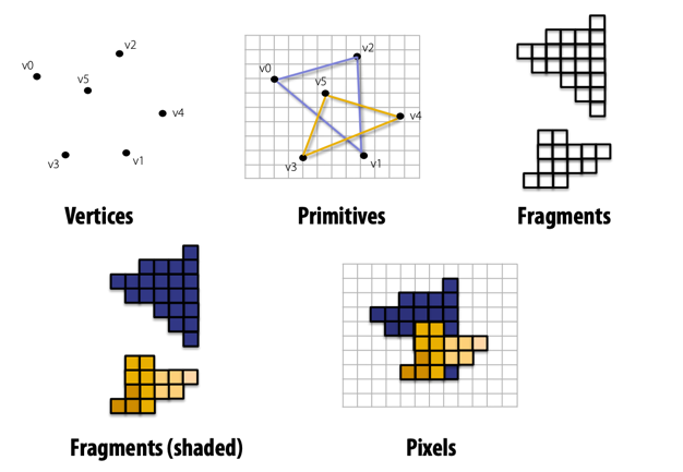
Figure 1. The graphics rendering pipeline [2]
2.1.3. Advantages, Disadvantages of GPU
GPUs are tailored for parallel computing, allowing multiple calculations or tasks to run simultaneously. GPUs have evolved from their initial role in 3D graphics to become highly flexible and programmable. GPUs enjoy widespread support from various deep learning frameworks and libraries, simplifying their integration into AI projects and making them accessible to developers.
But GPUs have the issue of limited memory bandwidth, which affects the speed at which data can move between the GPU's memory and its computation cores [3]. GPUs can be power-hungry, especially when running at maximum capacity, leading to increased operational costs compared to alternative AI accelerators like CPUs. GPUs also generate substantial heat during operation, necessitating efficient cooling solutions to prevent overheating. While GPUs excel at maximizing throughput by efficiently processing batches of tasks concurrently, they may not offer the lowest latency for individual tasks.
2.2. FPGA
2.2.1. Definition of FPGA
An FPGA (Field-Programmable Gate Array) is an integrated circuit that can be programmed or reconfigured after its initial manufacturing. It consists of an array of programmable logic blocks and interconnections that can be customized to perform various digital tasks
2.2.2. Basic Principle of FPGA operation
Logic-block Architecture: A Configurable Logic Block (CLB) serves as a fundamental component within an FPGA, providing the essential logic and storage capabilities necessary for a given application design. This core component can range from fine-grained transistors to coarse-grained processors, with trade-offs between resource efficiency and performance. The spectrum of basic logic blocks includes options like NAND gates, multiplexers, lookup tables (LUTs), and PAL-style wide input gates. LUT-based CLBs, employed by commercial vendors like Xilinx and Altera, strike a balance between granularity extremes, offering flexibility without excessive resource wastage. A basic logic element (BLE) typically consists of a LUT and a Flip-Flop, with a LUT-4, for instance, utilizing 16 SRAM bits to implement 4-input Boolean functions. CLBs can form clusters of interconnected BLEs, facilitating local routing networks for inter-BLE communication. While CLBs constitute the foundation, modern FPGAs often incorporate specialized blocks like memory, multipliers, and DSP blocks, optimized for specific tasks, but potentially leading to resource inefficiencies when unused [4].
Routing Architecture: In FPGA architecture, the computing capabilities are provided by programmable logic blocks interconnected through a configurable routing network. This network, comprising wires and programmable switches, is essential for implementing user-defined circuits. To cater to the diverse routing needs of different digital circuits, FPGA routing interconnects must be highly adaptable. While routing requirements vary, many designs exhibit a preference for short wires due to their locality, but they also require some longer connections. Therefore, designing FPGA routing interconnects must strike a balance between flexibility and efficiency. The organization of routing resources in relation to logic block placement, referred to as global routing architecture, greatly impacts overall efficiency. Additionally, the specific configuration of switch blocks at a detailed level, known as detailed routing architecture, plays a crucial role. The Architecture of FPGA is shown in figure 2.
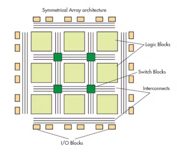
Figure 2. The Architecture of FPGA [4]
2.2.3. Advantages, Disadvantages of FPGA
FPGAs excel in time-critical applications like software-defined radio, medical devices, and mil-aero systems, making FPGAs more versatile for prototyping than ASICs. FPGAs also shine in parallel processing, ideal for tasks involving extensive data processing, such as embedded vision and measurement systems. FPGAs are reconfigurable chips, allowing their internal logic to be modified via software updates, bug fixes, or support for new protocols [5].
But FPGAs are costlier than microcontrollers or ASICs, especially in high-volume production scenarios, as the per-unit cost tends to be higher. FPGAs typically consume more power than ASICs and microcontrollers, which may be a concern in power-sensitive applications. The design process for FPGAs can be more intricate, demanding specialized expertise in hardware design, HDL, synthesis, and place-and-route tools.
2.3. ASIC
2.3.1. Definition of ASIC
An application-specific integrated circuit is an integrated circuit (IC) that's custom-designed for a particular task or application.
2.3.2. Basic Principle of ASIC operation
The working principle of ASIC chips is similar to regular integrated circuits, as they are both composed of multiple logic gates (such as AND gates, OR gates, NOT gates, etc.) and memory units (such as registers, TPS2051BDBVR memory, etc.). ASIC chips can be designed and manufactured according to specific application requirements, which allows them to have higher performance and lower power consumption. The workflow of an ASIC chip is roughly as follows: Input Signals: The ASIC chip receives input signals such as data, clock, control signals, etc; Logical Operations: The ASIC chip performs logical operations such as AND, OR, NOT, etc; Data Storage: The ASIC chip stores the calculation results in registers, memory units, and so on; Output Signals: The ASIC chip outputs the computed results, such as data, status signals, etc.
The design of an ASIC is carried out step by step, following a sequence known as the ASIC design flow [6]. The following flowchart outlines the steps of the design process:1. Design Input: In this step, the design's microarchitecture is implemented using hardware description languages like VHDL, Verilog, and System Verilog. 2. Logic Synthesis: During this stage, a netlist of the logic units to be used, along with interconnects and all other required components, is prepared using HDL. 3. System Partitioning: In this step, the larger-sized chip is divided into ASIC-sized portions. 4. Pre-layout Simulation: Simulation testing is performed at this stage to check for design errors. 5. Layout Planning: The netlist blocks are arranged on the chip in this step. 6. Placement: The positions of the units within the blocks are determined.7. Routing: Connections are established between blocks and units in this step. 8. Extraction: Electrical characteristics like resistance and capacitance values of the interconnects are determined. 9. Post-layout Simulation: This simulation is carried out to ensure that the system operates correctly under interconnect loads before manufacturing models are submitted. The ASIC design flow ensures that the ASIC is designed systematically and thoroughly, from the initial architectural design to the final testing and verification stages, before it goes into production. The Design step of ASIC is shown in figure 3.
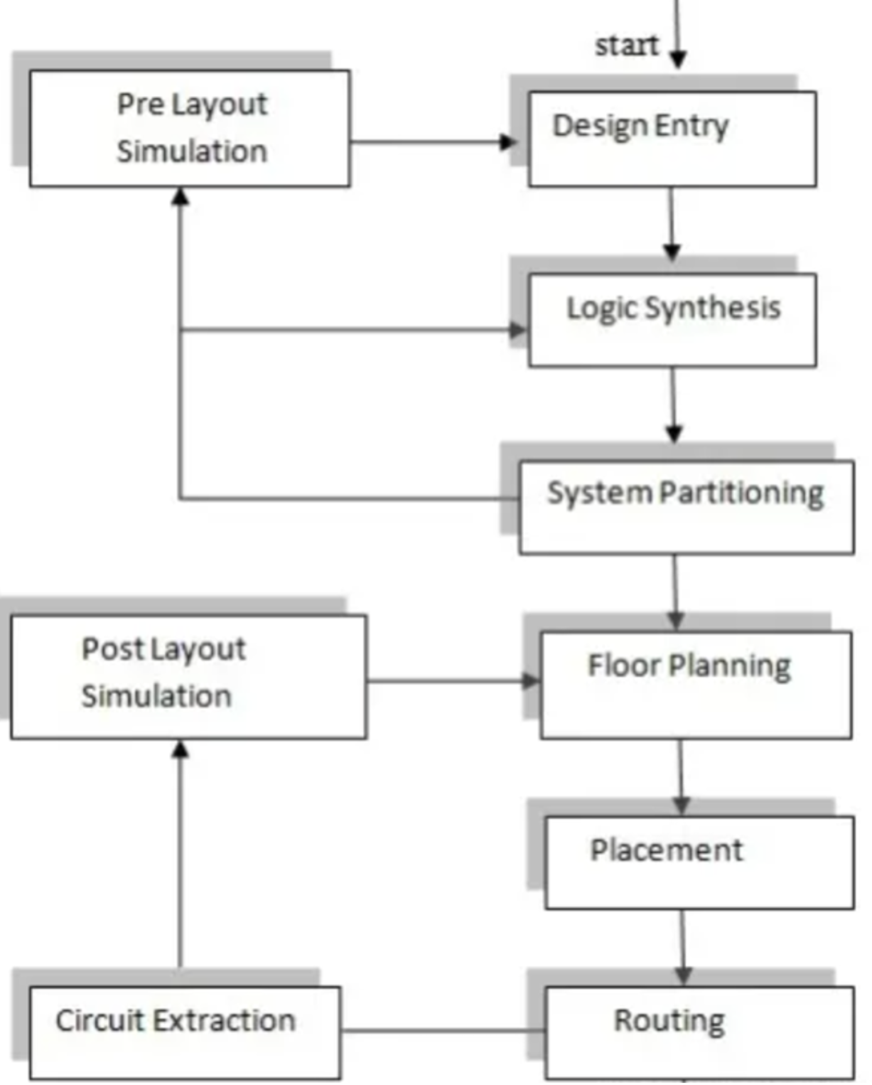
Figure 3. The Design step of ASIC [6]
2.3.3. Advantages, Disadvantages of ASIC
ASICs have significantly lower unit costs for high-volume designs, making it more cost-effective than FPGA implementation. ASICs provide faster performance and design flexibility, allowing for extensive speed optimizations. ASICs can be optimized for low power consumption, employing techniques like power gating, clock gating, and pipelining to achieve power efficiency.
But ASICs have lengthy development timelines, with some large ASICs taking a year or more to design. Designers must also address issues like Design for Manufacturability (DFM) and Signal Integrity, which are not as critical in FPGA development. ASIC design tools are expensive, requiring a substantial investment in Non-Recurring Engineering (NRE) costs [7].
2.4. Compare GPU, FPGA, and ASIC in a Chart
The Compare GPU, FPGA, and ASIC is shown in the table 1.
Table 1. Comparing GPU, FPGA, and ASIC.
Accelerator | GPU | FPGA | ASIC |
Overview | Initially intended for graphics and videos, these chips are now employed in a diverse array of computationally demanding tasks. | An integrated circuit that can be programmed or reconfigured after its initial manufacturing. | An integrated circuit (IC) that's custom-designed for a particular task or application. |
Strengths | Parallel computing; Flexible and programmable; Widespread support | Low latency; Adaptable; Parallel computing; reconfigurable | Lower unit cost; optimum performance and power consumption |
Weaknesses | Bottleneck; High power consumption; Generate substantial heat; May not offer lowest latency for individual task | Expensive in large production; Consume more power than ASIC; | Take long time to the market; Expensive design tools; Some design issues |
3. Application Analysis
3.1. Application Analysis for GPU
3.1.1. GPU CUDA programming in Medical Image Analysis
According to a research did by T. Kalaiselvi, P. Sriramakrishnan, K. Somasundaram, the application of GPUs (Graphics Processing Units) in medical image analysis is crucial due to the growing complexity of medical data and the need for high computational power [8]. In the field of medical image analysis, GPUs play a vital role in various aspects:
Image Denoising: Medical images, particularly those from MRI, often suffer from random noise introduced during acquisition, measurement, and transmission. Denoising algorithms, such as adaptive filtering, anisotropic diffusion, bilateral filtering, and non-local means filter, are used to enhance image quality and reveal hidden details. GPUs accelerate these denoising algorithms by leveraging data parallelism, making them efficient for processing large datasets.
Image Registration: Medical image registration is essential for aligning images from different modalities or time points, enabling accurate diagnosis and surgical planning. GPUs are particularly useful for image registration because they can accelerate operations like linear interpolation. Popular registration algorithms like block matching algorithm (BMA) and rigid transformation estimation (RTE) benefit from GPU hardware support.
Segmentation: Segmentation of medical images, which involves identifying and isolating specific structures or regions of interest (e.g., tumors, blood vessels, or bones), can be computationally intensive, especially with large datasets. GPUs can significantly speed up segmentation methods such as thresholding, region growing, morphology, and watershed, making them suitable for clinical applications that require both speed and accuracy.
Visualization: Visualization is a crucial component of medical image processing, as it allows healthcare professionals to interpret complex 2D, 3D, or 4D imaging datasets more effectively. GPUs are instrumental in creating real-time 3D visualizations of large medical datasets, improving diagnostic accuracy and surgical planning. Visualization techniques can be broadly categorized into surface rendering and volume rendering, both of which benefit from the parallel processing capabilities of GPUs.
3.1.2. Advanced GPU Ray casting
According to a research did by Henning Scharsach, GPU-based raycasting represents a paradigm shift in the realm of volume rendering and interactive 3D visualization. This technology capitalizes on the inherent strengths of modern graphics processing units, such as parallelism, fast memory access, and dedicated graphical instructions, to provide real-time rendering capabilities that were previously unattainable with CPU-based approaches. The optimizations discussed in the paper, including empty space skipping, hitpoint refinement, and geometry intersection, not only enhance rendering speed but also contribute to improved image quality, making this approach particularly suitable for applications in medical imaging, scientific research, and computer graphics [9].
One of the key advantages of GPU-based raycasting is its versatility. It allows for a wide range of applications beyond traditional volume rendering, including interactive fly-through simulations, augmented reality, and the integration of 3D models into real-world scenes. This technology opens up new possibilities for medical diagnosis, virtual endoscopy, and immersive data exploration, enabling users to interact with complex 3D datasets in real time.
Researchers and developers can continue to refine and optimize these techniques, making them even more memory-efficient and adaptable to different types of datasets. Moreover, advancements in GPU hardware will likely further enhance the capabilities of this technology, enabling the handling of even larger and more complex datasets. As a result, GPU-based raycasting is poised to play a pivotal role in advancing fields that rely on interactive and realistic 3D visualization, with the potential to revolutionize how we explore and interact with 3D data.
3.2. Application Analysis for FPGA
3.2.1. Neural Network Implementation Using FPGA
In this paper, the authors discuss the implementation of a single neuron in FPGA and address various issues related to hardware realization of neural networks. They focus on efficient implementation techniques, particularly for multi-input neurons with linear and nonlinear excitation functions. The paper also proposes a method for handling signed decimal numbers and improving the speed of operation using lookup tables (LUTs) [10].
This paper has delved into the intricate challenges and viable solutions linked to FPGA-based implementations of neural networks, underscoring the need for optimizing computational blocks, judicious resource allocation, and careful consideration of bit precision. Furthermore, it has provided a tangible illustration of FPGA's practical application in the development of a Space Vector Modulator for a Voltage Source Inverter. This case study vividly demonstrates FPGA's adaptability and versatility in enhancing the performance of complex systems, especially those reliant on parallel processing, rapid reconfiguration, and high-speed computation. In a rapidly evolving technological landscape, FPGA technology remains a cornerstone for engineers and researchers across an array of scientific and engineering domains, empowering them to push the boundaries of innovation and performance optimization in hardware-based applications.
3.2.2. FPGA in Aerospace Application
The paper discusses the challenges of using SRAM-based Field Programmable Gate Arrays (FPGAs) in aerospace applications, where radiation-induced faults, particularly Single Event Upsets (SEUs), can be problematic. It introduces a methodology for addressing these challenges using Xilinx XC4000 series FPGAs. The methodology follows a hierarchy of detection, mitigation, and correction:
Fault Identification and Mitigation: It starts by configuring three FPGAs identically and running them in parallel. A 3-State Voter compares their outputs to identify faults. If an issue is found, the faulty FPGA's outputs are disabled, and a redundant FPGA takes over without interrupting the system.
Soft-Fault Judgment and Correction: Readback capabilities of Xilinx FPGAs are used to assess configuration memory integrity. Soft faults or SEUs are detected, and corrective actions are taken to reconfigure the faulty FPGA.
Hard-Fault Location and Bypass: While rare, the methodology includes steps to locate and bypass hard faults under the control of a microcontroller.
The paper highlights the significance of FPGA technology in aerospace and offers a practical approach to enhance fault tolerance, ensuring continuous system operation in the presence of radiation-induced faults. It also suggests future work exploring newer FPGA series like Virtex for potential improvements in fault mitigation techniques [11].
3.3. Application for ASIC
3.3.1. Bitcoin Mining Using ASIC
BonanzaMine is a cutting-edge Application-Specific Integrated Circuit (ASIC) designed for Bitcoin mining, offering remarkable energy efficiency and high-performance capabilities. This ASIC operates at an incredibly low voltage of 355mV, significantly reducing energy consumption, a critical factor in Bitcoin mining economics.
Key features of BonanzaMine include a specialized message digest datapath optimized for Bitcoin's SHA256 double hash algorithm, resulting in a 33% reduction in dynamic power consumption compared to conventional implementations. It also employs a half-frequency scheduler datapath, further cutting power usage by 33% [12].
The ASIC utilizes a latch-based design, eliminating minimum-delay paths, simplifying the clocking system, and reducing sequential and clock power by 50%. Each BonanzaMine ASIC houses 258 mining engines, operating in parallel to compute SHA256 double hashes, resulting in impressive mining throughput.
Furthermore, its ability to operate at a range of voltages and adapt to changing energy cost scenarios allows miners to optimize energy efficiency. The system is composed of multiple hash boards, an Intel FPGA-based control unit, power supply, and cooling system, providing a self-contained solution capable of delivering a hash rate of 40THash/s while adhering to a thermal design power envelope of 3600W.
Manufactured using a 7nm CMOS process, BonanzaMine operates efficiently at frequencies between 1.35GHz to 1.6GHz and maintains an outstanding energy efficiency of 55J/THash. BonanzaMine represents a significant leap in ASIC technology for Bitcoin mining, offering miners a cost-effective solution to reduce operational expenses associated with energy consumption while achieving high mining throughput.
3.3.2. CAN-Based Aging Monitoring Technique for Automotive ASICs
In the rapidly evolving landscape of the automobile industry, the integration of self-driving technology and electronic components is becoming increasingly prevalent. This transition has led to a growing reliance on automotive Application-Specific Integrated Circuits (ASICs) to drive various vehicle functions, from safety features to enhanced fuel efficiency. However, despite the shift towards electronics, vehicles still require periodic maintenance to ensure their optimal functioning, both for mechanical parts and automotive electronics. To address this need for reliability, the paper proposes a Controller Area Network (CAN)-based Test Access Mechanism (TAM) for automotive ASICs. This mechanism not only enables regular maintenance but also tackles the critical issue of aging-induced defects, which can manifest in ASICs due to factors like temperature fluctuations and stress. These defects, difficult to detect with conventional in-field diagnostic techniques, can lead to performance degradation or even critical failures in automotive electronics [13].
To elaborate further on the proposed solution, the paper introduces an efficient aging monitoring scan flip-flop with soft-error resilience. This innovation enhances the ability to identify aging-induced defects, ensuring the continued reliability of automotive semiconductors throughout their lifecycle. The CAN-based TAM facilitates periodic maintenance and diagnostics, even after these chips are integrated into vehicles. In doing so, it addresses the challenges of detecting and diagnosing aging-related issues, which are crucial for maintaining the safety and functionality of modern automotive electronics. Overall, this work offers a comprehensive approach to safeguarding the reliability of automotive ASICs, ensuring they continue to perform optimally as electronic components become increasingly integral to the automotive industry.
4. Conclusion
GPU, FPGA, and ASIC stand out as the primary AI acceleration technologies, each distinguished by its distinct operational principles and a set of strengths and weaknesses that render them suitable for diverse applications. GPU CUDA programming has revolutionized medical image analysis, empowering tasks such as image denoising, image registration, segmentation, and visualization. These parallel processors effectively enhance image quality, align disparate images, expedite segmentation processes, and enable real-time 3D visualizations, bolstering medical diagnoses and surgical planning. Moreover, advanced GPU ray casting has ushered in a new era of interactive 3D visualization, with applications spanning medical imaging, scientific research, and augmented reality, promising innovative advancements in medical diagnostics and immersive data exploration. On the FPGA front, neural network implementation underscores FPGA's prowess in optimizing computational blocks for hardware-based neural networks. Additionally, FPGA finds practical application in aerospace, addressing radiation-induced faults through fault identification, mitigation, and correction strategies, ensuring uninterrupted system operation. Lastly, ASICs have showcased their prowess in Bitcoin mining, boasting remarkable energy efficiency and high-performance capabilities. This ASIC represents a significant leap forward, offering a cost-effective solution for miners aiming to reduce energy consumption while achieving high mining throughput. In the automotive industry, ASICs find utility in aging monitoring techniques, ensuring the reliability of automotive semiconductors amidst the integration of electronic components into vehicles. This comprehensive approach safeguards the functionality and safety of modern automotive electronics, marking a pivotal development in ASIC technology.
The global artificial intelligence chip market was valued at $11.2 billion in 2021 and is projected to reach $263.6 billion by 2031, growing at CAGR of 37.1% from 2022 to 2031. The development of AI chips is fast due to the rise of quantum computing and increased adoption of AI chips in robotics. Additionally, the market is expected to offer substantial growth prospects with the growing availability of autonomous robots from various companies. AI accelerators have a promising future: they excel in high-performance computing, edge computing for reduced latency, robotics for advanced tasks, and bolster security through rapid data analysis, especially in cybersecurity. However, AI accelerator development faces challenges like enhancing energy efficiency, optimizing for diverse workloads, and overcoming memory limitations. Achieving sustainable and secure integration across industries while managing privacy and ethical concerns is crucial for their future success.
References
[1]. Zhou G, Feng Y, Bo R, et al. GPU-accelerated batch-ACPF solution for N-1 static security analysis. IEEE Transactions on Smart Grid, 2016, 8(3): 1406-1416.
[2]. Hacker C, Aizenberg I, Wilson J. GPU simulator of multilayer neural network based on multi-valued neurons. 2016 International Joint Conference on Neural Networks (IJCNN). IEEE, 2016: 4125-4132.
[3]. Agullo E, Augonnet C, Dongarra J, et al. Dynamically scheduled Cholesky factorization on multicore architectures with GPU accelerators. Symposium on Application Accelerators in High Performance Computing (SAAHPC). 2010.
[4]. Bailey D G. Design for embedded image processing on FPGAs. John Wiley & Sons, 2023.
[5]. Zhang K, Chang Y, Chen M, et al. Computer organization and design course with FPGA cloud. Proceedings of the 50th ACM Technical Symposium on Computer Science Education. 2019: 927-933.
[6]. Trigilio P, Busca P, Quaglia R, et al. A SiPM-readout ASIC for SPECT applications. IEEE Transactions on Radiation and Plasma Medical Sciences, 2018, 2(5): 404-410.
[7]. Skup K R, Orleański P, Nowosielski W, et al. Mixed signal ASIC controller for satellite medium power DC/DC converters.2015 22nd International Conference Mixed Design of Integrated Circuits & Systems (MIXDES). IEEE, 2015: 359-363.
[8]. Kalaiselvi T, Sriramakrishnan P, Somasundaram K. Survey of using GPU CUDA programming model in medical image analysis. Informatics in Medicine Unlocked, 2017, 9: 133-144.
[9]. Scharsach H. Advanced CPU Raycasting. 2005.
[10]. Muthuramalingam A, Himavathi S, Srinivasan E. Neural network implementation using FPGA: issues and application. International Journal of Electrical and Computer Engineering, 2008, 2(12): 2802-2808.
[11]. Li Y, Li D, Wang Z. A new approach to detect-mitigate-correct radiation-induced faults for SRAM-based FPGAs in aerospace application. Proceedings of the IEEE 2000 National Aerospace and Electronics Conference. NAECON 2000. Engineering Tomorrow (Cat. No. 00CH37093). IEEE, 2000: 588-594.
[12]. Suresh V B, Katta C S, Rajagopalan S, et al. Bonanza mine: An ultra-low-voltage energy-efficient Bitcoin mining ASIC. 2022 IEEE International Solid-State Circuits Conference (ISSCC). IEEE, 2022, 65: 354-356.
[13]. Kim J, Ibtesam M, Kim D, et al. CAN-Based aging monitoring technique for automotive ASICs with efficient soft error resilience. IEEE Access, 2020, 8: 22400-22410.
Cite this article
Shi,Y. (2024). Unveiling the powerhouses of AI: A comprehensive study of GPU, FPGA, and ASIC accelerators. Applied and Computational Engineering,50,97-105.
Data availability
The datasets used and/or analyzed during the current study will be available from the authors upon reasonable request.
Disclaimer/Publisher's Note
The statements, opinions and data contained in all publications are solely those of the individual author(s) and contributor(s) and not of EWA Publishing and/or the editor(s). EWA Publishing and/or the editor(s) disclaim responsibility for any injury to people or property resulting from any ideas, methods, instructions or products referred to in the content.
About volume
Volume title: Proceedings of the 4th International Conference on Signal Processing and Machine Learning
© 2024 by the author(s). Licensee EWA Publishing, Oxford, UK. This article is an open access article distributed under the terms and
conditions of the Creative Commons Attribution (CC BY) license. Authors who
publish this series agree to the following terms:
1. Authors retain copyright and grant the series right of first publication with the work simultaneously licensed under a Creative Commons
Attribution License that allows others to share the work with an acknowledgment of the work's authorship and initial publication in this
series.
2. Authors are able to enter into separate, additional contractual arrangements for the non-exclusive distribution of the series's published
version of the work (e.g., post it to an institutional repository or publish it in a book), with an acknowledgment of its initial
publication in this series.
3. Authors are permitted and encouraged to post their work online (e.g., in institutional repositories or on their website) prior to and
during the submission process, as it can lead to productive exchanges, as well as earlier and greater citation of published work (See
Open access policy for details).
References
[1]. Zhou G, Feng Y, Bo R, et al. GPU-accelerated batch-ACPF solution for N-1 static security analysis. IEEE Transactions on Smart Grid, 2016, 8(3): 1406-1416.
[2]. Hacker C, Aizenberg I, Wilson J. GPU simulator of multilayer neural network based on multi-valued neurons. 2016 International Joint Conference on Neural Networks (IJCNN). IEEE, 2016: 4125-4132.
[3]. Agullo E, Augonnet C, Dongarra J, et al. Dynamically scheduled Cholesky factorization on multicore architectures with GPU accelerators. Symposium on Application Accelerators in High Performance Computing (SAAHPC). 2010.
[4]. Bailey D G. Design for embedded image processing on FPGAs. John Wiley & Sons, 2023.
[5]. Zhang K, Chang Y, Chen M, et al. Computer organization and design course with FPGA cloud. Proceedings of the 50th ACM Technical Symposium on Computer Science Education. 2019: 927-933.
[6]. Trigilio P, Busca P, Quaglia R, et al. A SiPM-readout ASIC for SPECT applications. IEEE Transactions on Radiation and Plasma Medical Sciences, 2018, 2(5): 404-410.
[7]. Skup K R, Orleański P, Nowosielski W, et al. Mixed signal ASIC controller for satellite medium power DC/DC converters.2015 22nd International Conference Mixed Design of Integrated Circuits & Systems (MIXDES). IEEE, 2015: 359-363.
[8]. Kalaiselvi T, Sriramakrishnan P, Somasundaram K. Survey of using GPU CUDA programming model in medical image analysis. Informatics in Medicine Unlocked, 2017, 9: 133-144.
[9]. Scharsach H. Advanced CPU Raycasting. 2005.
[10]. Muthuramalingam A, Himavathi S, Srinivasan E. Neural network implementation using FPGA: issues and application. International Journal of Electrical and Computer Engineering, 2008, 2(12): 2802-2808.
[11]. Li Y, Li D, Wang Z. A new approach to detect-mitigate-correct radiation-induced faults for SRAM-based FPGAs in aerospace application. Proceedings of the IEEE 2000 National Aerospace and Electronics Conference. NAECON 2000. Engineering Tomorrow (Cat. No. 00CH37093). IEEE, 2000: 588-594.
[12]. Suresh V B, Katta C S, Rajagopalan S, et al. Bonanza mine: An ultra-low-voltage energy-efficient Bitcoin mining ASIC. 2022 IEEE International Solid-State Circuits Conference (ISSCC). IEEE, 2022, 65: 354-356.
[13]. Kim J, Ibtesam M, Kim D, et al. CAN-Based aging monitoring technique for automotive ASICs with efficient soft error resilience. IEEE Access, 2020, 8: 22400-22410.