


1. Introduction
Gallium Nitride (GaN) has been recognized as an exceptionally promising candidate in the realm of semiconductor materials, owing to its remarkable attributes and extensive applicability in electronic device technology. The unique properties and advantages of GaN have catalyzed substantial research and investigative efforts to unravel its potential across diverse disciplines [1]. A comprehensive grasp of the developmental trajectory, present status, inherent challenges, and future perspectives of GaN materials is imperative for propelling technological advancements and fulfilling global requisites for efficient and sustainable electronic solutions.
This exhaustive review endeavors to dissect the complex domain of GaN materials by scrutinizing their intrinsic properties, historical development, current state of advancement, and prospective future directions. The discourse includes an in-depth examination of the distinctive characteristics and benefits proffered by GaN materials, highlighting their critical role in the realm of electronic device applications, and retracing the evolution of synthesis methodologies for GaN materials. It further ventures into the current progresses in the investigation of GaN material properties, encompassing structural analysis, characterization of crystal imperfections, and studies on optical properties and optoelectronic device functionalities. Additionally, the review addresses ongoing research trends in the arenas of large-scale production techniques, design optimization for high-efficiency power devices, and initiatives aimed at augmenting the sustainability and environmental friendliness of GaN materials. Moreover, it addresses the substantial challenges encountered, including cost-related concerns, reliability issues, complexities in design, and the exigency for process optimization. Lastly, it envisages the future landscape and potential application sectors that could leverage the transformative attributes of GaN materials.
2. Basic analysis of GaN materials
2.1. GaN material properties and advantages, structure
GaN is a compound semiconductor material of group III-V with many properties and advantages. GaN can exist in different structural forms, including crystalline, thin film and heterostructures. These different structural forms provide flexibility and versatility for the application of GaN in different fields, making it one of the research hotspots in the field of semiconductor device fabrication. The structure of GaN is shown in Figure 1 (a) and Figure 1 (b). The following are some structural advantages of GaN.
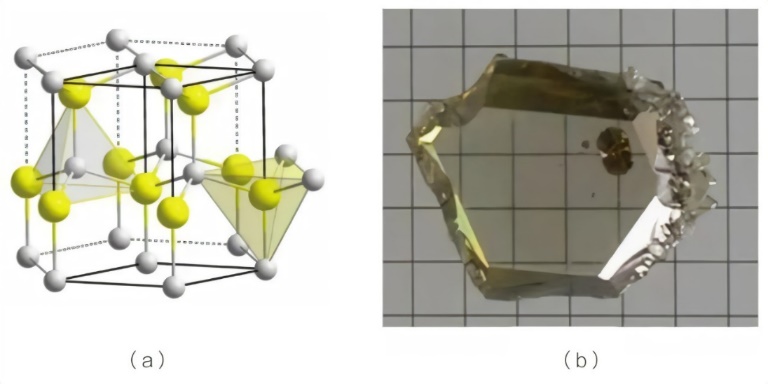
Figure 1. The structure of GaN [2].
Wide Bandgap Energy Gap: GaN has a large bandgap energy gap of approximately 3.4 eV, which provides a higher energy difference between the electronic energy band and the valence band compared to conventional materials such as silicon and germanium, allowing it to excel in high-power and high-frequency applications [2].
High Electron Flow Rate: GaN has a high electron saturation drift velocity, which is the maximum speed at which electrons can move through the material. The high electron flow rate allows GaN to operate at high frequencies for microwave, RF and power amplifier applications.
High Saturation Electron Mobility: GaN has a high saturation electron mobility, which is the maximum rate at which electrons can travel through the material. The high saturation electron mobility makes GaN perform well in high frequency applications, allowing for faster switching speeds and higher efficiencies.
2.2. Application of GaN materials in electronic devices
GaN is a kind of wide bandgap semiconductor material with many excellent properties, so it is widely used in the manufacture of electronic devices. The following are some common GaN materials used in electronic devices:
Power electronics: GaN is widely used in power electronics, such as high frequency switches, power amplifiers and converters. Due to GaN’s high saturation electron mobility and high breakdown field strength, it is able to provide higher efficiency and performance in high power density and high temperature environments [3].
Radio Frequency (RF) Devices: GaN is also widely used in RF applications, such as communication systems, radar systems, and amplifiers in the radio frequency band, etc. GaN’s high electron flow rate and good thermal conductivity make it ideal for high-power RF applications, enabling higher operating frequencies and lower power consumption.
Opto-electronic devices: GaN materials are also used in opto-electronic devices such as LEDs (light emitting diodes) and lasers, etc. GaN light-emitting devices have high luminous efficiencies and long lifetimes, and can be used in lighting, displays, and communications. GaN lasers [4]. On the other hand, have a narrow spectral linewidth and high power output, and are suitable for applications such as laser printing, optical communications and biomedicine.
2.3. Development history
The history of GaN materials dates back to the 1960s. There are the major milestones in the development of GaN materials: In 1969, American scientists Herbert P. Maruska and Jasprit Singh synthesised GaN crystals for the first time, and in 1987, a team of Japanese researchers succeeded in synthesising high-quality GaN films for the first time. 1993, Japanese company Nichia Chemical Industries succeeded in commercialising high-brightness blue light LEDs through an improved process of GaN material preparation. achieved the commercialisation of high-brightness blue LEDs. During the same period, other research institutes also made important contributions to the properties and applications of GaN materials. 2006, a US research team successfully fabricated the first high-power GaN-based RF electronic device using GaN materials. During this period, the research focus of GaN materials gradually shifted to the development and application of power electronic devices and RF devices. In 2014, a U.S. research team realised high-efficiency white LEDs in GaN materials, which opened up a wide range of applications of GaN materials in the field of lighting. During this period, GaN materials have made important progress in the field of power electronics and radio frequency, becoming an ideal choice for high-power, high-frequency electronic devices. During this period, GaN materials have made important progress in the field of power electronics and radio frequency, becoming an ideal choice for high-power and high-frequency electronic devices. The development history is shown in figure 2.
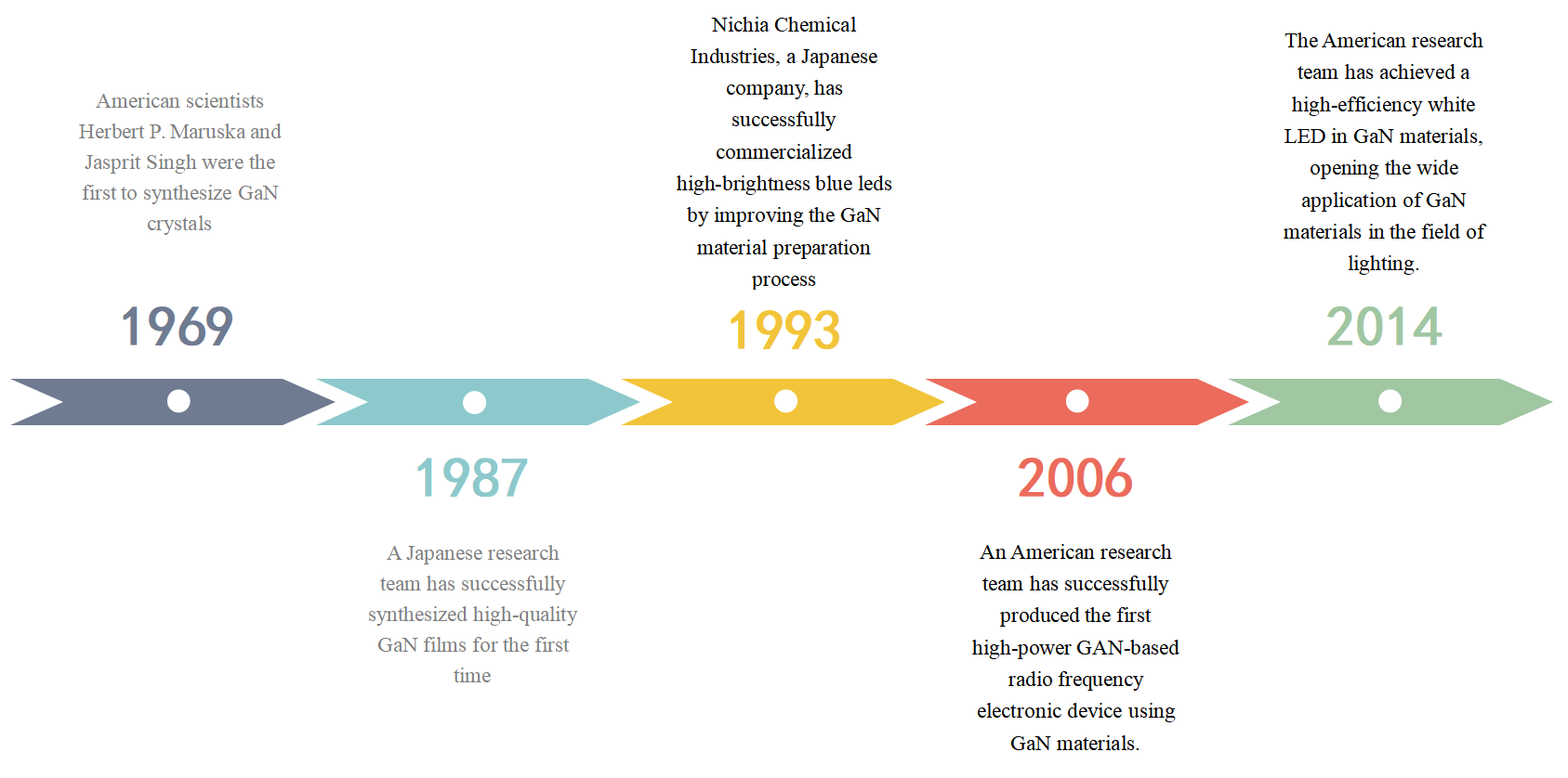
Figure 2. Development history (Photo/Picture credit: Original).
At the same time, the improvement and optimisation of the structure and growth methods of GaN materials also promoted their development in various applications [5].
With the continuous progress of technology and in-depth research, the application of GaN materials in the fields of LED lighting, communications, radar, wireless charging and solar energy has been rapidly developed. At present, GaN is still a research hotspot in the field of semiconductor materials, and there is more potential to be tapped in the future.
3. Development research and analysis of GaN materials
3.1. Progress in preparation technology of GaN materials
3.1.1. Gas phase epitaxy. Gas phase epitaxy of GaN materials is a commonly used preparation method for growing GaN thin films on the surface of substrates. The method can be summarised in the following steps: substrate preparation, reaction chamber environment preparation, raw material supply, pyrolysis and growth, cooling and crystallisation, and post-treatment. On GaN coated with a patterned mask, the GaN films were produced using either metalorganic vapour phase epitaxy (MOVPE) or hydride vapour phase epitaxy (HVPE) [6].
3.1.2. Hydrothermal process. Hydrothermal preparation of GaN materials is a commonly used method. Hydrothermal method means that the reaction solution or mixture is placed in a sealed container in the presence of water or other solvents at high temperature and pressure. For the hydrothermal preparation of GaN materials, the process may be as follows: first, a precursor solution of gallium nitride is prepared. Optionally, an inorganic salt or an organometallic compound may be used as the precursor material and dissolved in a suitable solvent. Next, the precursor solution is transferred to a sealed, high-pressure reaction vessel. Ensure that the reaction vessel is capable of withstanding the required high temperature and pressure conditions. The reaction vessel is then sealed and heated to the appropriate temperature. Meanwhile, during the heating process, the appropriate pressure is maintained and the reaction solution is kept stirred to promote the reaction. After a certain reaction time, the heating is stopped and the reaction vessel is cooled. This allows the growth and formation of GaN crystals in the reaction solution. Finally, the reaction product is filtered, washed and dried to obtain a pure GaN material.
3.1.3. Solution method. GaN preparation by solution method is a commonly used method, which can be achieved by dissolving the metal nitride precursor and making it deposited on the substrate under suitable conditions. Its preparation steps are preparation of metal nitride precursor, substrate preparation, solution preparation, deposition process, and annealing treatment.
3.2. Research progress of physical properties of GaN materials
3.2.1. Structure and crystal defect analysis. It has a hexagonal crystal system structure and consists of gallium and nitrogen atoms. In GaN crystals, lattice defects can have a significant impact on its properties and performance.
Common GaN crystal defects include point defects, line defects and surface defects. Point defects refer to individual atomic dislocations or vacancies that occur in the crystal, such as gallium dislocations, nitrogen dislocations, and nitrogen vacancies. These point defects can be detected and analysed by optical and electrical techniques [7]. Line defects are wire-like defects in crystals, such as helical dislocations and aligned faults. These line defects are usually caused by incomplete formation during crystal growth and can be observed and analysed by techniques such as transmission electron microscopy. Facet defects are planar defects in crystals, such as grain boundaries and stacking layer errors. A grain boundary is a boundary between two crystal particles with different lattice orientations, while a stacking layer error is an anomaly in the atomic stacking sequence in a crystal. These face defects can be studied by techniques such as high-resolution transmission electron microscopy and X-ray diffraction.
3.2.2. Optical properties and optoelectronic device performance. GaN materials have many excellent optical properties and optoelectronic device performance.
Optical properties: GaN has a wide bandgap, making it highly responsive to ultraviolet light. GaN has high transparency, which can be applied to the preparation of transparent electrodes or optical windows. GaN has a high refractive index, which is conducive to the guidance and transmission of light. GaN materials can be doped with different impurities to achieve luminescence, and therefore are widely used in LEDs (light-emitting diodes) and lasers, etc [8].
The optical device performance: GaN materials have high electron mobility, which facilitates high-speed electron transport, and is therefore suitable for high-frequency and high-power applications.
Optoelectronic device performance: GaN materials have high electron mobility, which is conducive to high-speed electron transport, and therefore suitable for high-frequency and high-power applications. GaN materials have a high carrier saturation drift speed, which helps to improve the device switching speed and operating frequency.
GaN materials have good thermal stability and high temperature resistance, making it possible to maintain good electrical performance in high temperature environments. The high saturation drift speed and high refractive index of GaN materials make them suitable for high power devices, such as power amplifiers and high frequency switches.
3.3. Research trends of GaN materials
3.3.1. Development of large-scale preparation technology. In recent years, many researches and innovations have been conducted for the development of large-scale preparation techniques for GaN materials. The following are several common techniques for large-scale preparation of GaN materials:
Hydrothermal method: Hydrothermal method is a method to generate GaN crystals by reacting metallic aluminium with ammonia or nitride. This method has the advantages of simplicity, low cost and high purity, but the crystal growth rate is slow.
Vapour phase deposition: Vapour phase deposition methods are divided into metal organic chemical vapour deposition (MOCVD) and molecular beam epitaxy (MBE). Both methods can deposit high quality GaN films on the substrate. They have the advantages of fast growth rate, good control, and can achieve the growth of multilayer films.
Sputtering: Sputtering is used to dissociate atoms from a target surface by bombarding the target surface with ions or neutral particles and depositing them on the substrate. This method enables the preparation of GaN thin films on large area substrates with high growth rate, better control and uniformity [9].
With the continuous development of technology, the research on large-scale preparation technology of GaN materials is still in progress. New preparation methods and processes continue to emerge, providing a broader prospect for the application of GaN materials.
3.3.2. Design and optimization of energy efficient devices. GaN materials are widely used in the design and optimisation of high efficiency energy devices. Following are some important aspects of GaN materials for the design and optimisation of high-efficiency energy devices:
High Electron Mobility: GaN materials have high electron mobility, which makes them exhibit excellent properties in power devices. The electron mobility can be further improved by optimising the crystal structure and controlling the impurity concentration.
Two-dimensional electron gas: GaN materials form a two-dimensional electron gas at the interface, which is critical to device performance. By adjusting the surface state density and interfacial quality of the material, the electron gas migration characteristics and carrier concentration can be improved [10].
Thermal stability: GaN materials have good thermal stability and can operate in high temperature environments. This gives GaN devices an advantage in high-power applications and makes it easier to design for heat dissipation.
3.3.3. Sustainable and environmentally friendly performance improvements. GaN materials have the potential for a number of improvements in sustainability and environmentally friendly properties. The first is an improvement in energy efficiency: GaN materials have high electron mobility and low leakage currents, which makes them more efficient for energy conversion in power electronic devices. By using devices made from GaN materials, energy waste can be reduced and system efficiency can be improved. Secondly, it saves resources: GaN materials allow for smaller size and lighter weight device designs than traditional silicon materials. This not only reduces the use of resources, but also reduces waste generation. It also offers long life and stability: GaN materials have excellent thermal conductivity and can effectively dissipate heat, thus extending the life of the device. In addition, GaN materials are highly resistant to environmental conditions such as high temperature, humidity and radiation, making them more stable and reliable in a variety of applications.
4. Challenges and prospects of GaN materials
4.1. Cost and reliability issues
Firstly, there is the issue of cost. At present, the production cost of GaN materials is relatively high, mainly due to the use of complex equipment and processes in the manufacturing process and the high cost of the materials themselves. However, with the advancement of technology and the realisation of scale effect, it is expected that the cost of GaN materials will gradually decrease.
The next issue is reliability. Although GaN materials have excellent electronic properties, such as high electron mobility and high saturation drift rates, it still has some challenges in terms of reliability. A common problem is the lattice mismatch nature of GaN materials, which can lead to crystal defects and stress accumulation, thus affecting the long-term stability of the device. In addition, GaN materials face challenges in thermal management and packaging, as heat in high-power applications puts additional stress on materials and devices [11]. However, with continued progress in research and engineering, efforts are being made to address the reliability of GaN materials.
4.2. Design and process optimization requirements
Enhancement of material properties: The design and process optimisation of GaN materials should aim to enhance their properties, such as increasing current-carrying capacity, improving electrical conductivity and thermal characteristics. This can be achieved by optimising the material’s components, crystal structure and preparation methods.
Reducing preparation costs: GaN materials are expensive to prepare, so ways to reduce costs should be sought. For example, consider using more cost-effective feedstocks, improving growth techniques to reduce waste and increase yields.
Improve material stability and reliability: GaN materials have good performance in high-power and high-temperature environments, but they are also susceptible to factors such as stress, fatigue and oxidation. Attention should be given to improving material stability and reliability to ensure stable long-term performance.
Enabling size and shape control: The size and shape of GaN materials are important for different applications. Design and process optimisation should enable precise control of material size and shape for different applications.
4.3. Future development prospects and potential application areas
GaN materials have a broad development prospect and potential application areas in the future. For example:
Optoelectronic devices: GaN materials have excellent optoelectronic properties and can be used to manufacture high-brightness LEDs, as well as for applications such as lighting, displays, and car lights. In addition, they can be used to manufacture lasers, photodetectors and optical communication devices.
Power electronics: Because GaN materials have a high electron saturation migration rate and a high breakdown field strength, it can be used to make highly efficient, high power density power switching devices. This includes applications for electric vehicles, solar inverters, server power supplies, and more [12].
RF Devices: The high electron mobility and high breakdown field strength of GaN materials make them ideal for use in radio frequency (RF) amplifier devices. This will help improve the performance of wireless communications, radar and satellite communications systems, and drive the development of new technologies such as 5G and millimetre wave communications.
5. Conclusion
In conclusion, Gallium Nitride (GaN) has emerged as a highly promising material for electronic devices due to its unique characteristics and advantageous properties. Its wide bandgap, high breakdown voltage, and electron mobility make it suitable for various applications in the field of electronics. The development of GaN material has seen significant progress in terms of preparation techniques, including advancements in vapor-phase epitaxy, hydrothermal and solution methods, and other emerging fabrication approaches. Moreover, extensive research on the material’s physical properties has led to a better understanding of its structural characteristics, crystal defects, optical behavior, and performance in optoelectronic devices.
Looking ahead, the focus of GaN material research is shifting towards large-scale production methods, the design and optimization of high-efficiency power devices, and enhancing sustainability and environmental friendliness. However, challenges such as cost, reliability, and the need for improved design and processing techniques must be addressed to fully realize the potential of GaN materials. Despite these challenges, the future prospects for GaN materials are bright, with potential applications in various fields such as power electronics, communication systems, lighting, and sustainable energy solutions. As research continues, the ongoing efforts to overcome challenges and capitalize on the potential of GaN materials are expected to lead to continued advancements and broadened applications in the near future.
References
[1]. Ueda D. Properties and advantages of gallium nitride. Power GaN Devices: Materials, Applications and Reliability, 2017: 1-26.
[2]. Wang Z, Wang G, Liu X, et al. Two-dimensional wide band-gap nitride semiconductor GaN and AlN materials: properties, fabrication and applications. Journal of Materials Chemistry C, 2021, 9(48): 17201-17232.
[3]. Ajayan J, Nirmal D, Mohankumar P, et al. Challenges in material processing and reliability issues in AlGaN/GaN HEMTs on silicon wafers for future RF power electronics & switching applications: A critical review. Materials Science in Semiconductor Processing, 2022, 151: 106982.
[4]. Pan Y. Influence of N‐vacancy on the electronic and optical properties of bulk GaN from first‐principles investigations. International Journal of Energy Research, 2021, 45(10): 15512-15520.
[5]. Mori Y, Imanishi M, Murakami K, et al. Recent progress of Na-flux method for GaN crystal growth. Japanese Journal of Applied Physics, 2019, 58(SC): SC0803.
[6]. Siche D, Zwierz R. Growth of bulk gan from gas phase. Crystal Research and Technology, 2018, 53(5): 1700224.
[7]. Lyons J L, Wickramaratne D, Van de Walle C G. A first-principles understanding of point defects and impurities in GaN. Journal of Applied Physics, 2021, 129(11).
[8]. Monemar B, Bergman J P, Buyanova I A. Optical characterisation of GaN and related materials. GaN and related materials. CRC Press, 2021: 85-139.
[9]. Furqan C M, Ho J Y L, Kwok H S. GaN thin film: growth and characterizations by magnetron sputtering. Surfaces and Interfaces, 2021, 26: 101364.
[10]. Cao Y, Guan Q, Jia W, et al. Effect of strain on the effective mass of GaN and the mobility of AlGaN/GaN two-dimensional electron gas. Materials Today Communications, 2023, 35: 105788.
[11]. Meneghini M, De Santi C, Abid I, et al. GaN-based power devices: Physics, reliability, and perspectives. Journal of Applied Physics, 2021, 130(18).
[12]. Ueda T. GaN power devices: current status and future challenges. Japanese Journal of Applied Physics, 2019, 58(SC): SC0804.
Cite this article
Gao,H. (2024). Advancements and future prospects of Gallium Nitride (GaN) in semiconductor technology. Applied and Computational Engineering,65,37-44.
Data availability
The datasets used and/or analyzed during the current study will be available from the authors upon reasonable request.
Disclaimer/Publisher's Note
The statements, opinions and data contained in all publications are solely those of the individual author(s) and contributor(s) and not of EWA Publishing and/or the editor(s). EWA Publishing and/or the editor(s) disclaim responsibility for any injury to people or property resulting from any ideas, methods, instructions or products referred to in the content.
About volume
Volume title: Proceedings of Urban Intelligence: Machine Learning in Smart City Solutions - CONFSEML 2024
© 2024 by the author(s). Licensee EWA Publishing, Oxford, UK. This article is an open access article distributed under the terms and
conditions of the Creative Commons Attribution (CC BY) license. Authors who
publish this series agree to the following terms:
1. Authors retain copyright and grant the series right of first publication with the work simultaneously licensed under a Creative Commons
Attribution License that allows others to share the work with an acknowledgment of the work's authorship and initial publication in this
series.
2. Authors are able to enter into separate, additional contractual arrangements for the non-exclusive distribution of the series's published
version of the work (e.g., post it to an institutional repository or publish it in a book), with an acknowledgment of its initial
publication in this series.
3. Authors are permitted and encouraged to post their work online (e.g., in institutional repositories or on their website) prior to and
during the submission process, as it can lead to productive exchanges, as well as earlier and greater citation of published work (See
Open access policy for details).
References
[1]. Ueda D. Properties and advantages of gallium nitride. Power GaN Devices: Materials, Applications and Reliability, 2017: 1-26.
[2]. Wang Z, Wang G, Liu X, et al. Two-dimensional wide band-gap nitride semiconductor GaN and AlN materials: properties, fabrication and applications. Journal of Materials Chemistry C, 2021, 9(48): 17201-17232.
[3]. Ajayan J, Nirmal D, Mohankumar P, et al. Challenges in material processing and reliability issues in AlGaN/GaN HEMTs on silicon wafers for future RF power electronics & switching applications: A critical review. Materials Science in Semiconductor Processing, 2022, 151: 106982.
[4]. Pan Y. Influence of N‐vacancy on the electronic and optical properties of bulk GaN from first‐principles investigations. International Journal of Energy Research, 2021, 45(10): 15512-15520.
[5]. Mori Y, Imanishi M, Murakami K, et al. Recent progress of Na-flux method for GaN crystal growth. Japanese Journal of Applied Physics, 2019, 58(SC): SC0803.
[6]. Siche D, Zwierz R. Growth of bulk gan from gas phase. Crystal Research and Technology, 2018, 53(5): 1700224.
[7]. Lyons J L, Wickramaratne D, Van de Walle C G. A first-principles understanding of point defects and impurities in GaN. Journal of Applied Physics, 2021, 129(11).
[8]. Monemar B, Bergman J P, Buyanova I A. Optical characterisation of GaN and related materials. GaN and related materials. CRC Press, 2021: 85-139.
[9]. Furqan C M, Ho J Y L, Kwok H S. GaN thin film: growth and characterizations by magnetron sputtering. Surfaces and Interfaces, 2021, 26: 101364.
[10]. Cao Y, Guan Q, Jia W, et al. Effect of strain on the effective mass of GaN and the mobility of AlGaN/GaN two-dimensional electron gas. Materials Today Communications, 2023, 35: 105788.
[11]. Meneghini M, De Santi C, Abid I, et al. GaN-based power devices: Physics, reliability, and perspectives. Journal of Applied Physics, 2021, 130(18).
[12]. Ueda T. GaN power devices: current status and future challenges. Japanese Journal of Applied Physics, 2019, 58(SC): SC0804.