


1. Introduction
With the development of the times, semiconductor materials have entered the third-generation semiconductor era. The third-generation semiconductor materials are led by wide bandgap materials such as SiC and GaN. The maturity of wide bandgap technology provides enormous opportunities to ameliorate fast switching capabilities, high blocking voltage abilities, and high temperature operating conditions for power devices [1]. SiC can be applied to make power electronic devices such as MOSFET and IGBT, while GaN is applied to HEMT components. SiC MOSFET is replacing Si IGBT, for its their great conduction resistance, switching speed, and wide operating temperature range [2]. GaN MOSFET also has high potential in Power Switch for its low loss of energy [3]. These components are widely used in a large number of radiation resistant and high-temperature resistant materials, for satellite communication, power electronics, aerospace and other fields.
But these materials also face many challenges now. The production of third-generation semiconductor materials is a major constraint on their development. But currently, third-generation semiconductors have significant performance advantages compared to previous semiconductors, so the development prospects of third-generation semiconductors are very broad. Firstly, this paper provides a detailed analysis of the structure, conductive mechanism, working principle, and characteristic curves of MOSFET and HEMT. Afterwards, the advantages and disadvantages of both were analyzed through examples, and their application scenarios were analysed. The development of semiconductor materials and their constituent electronic components.
2. Basic Analysis
2.1. Structure of MOSFET and its working principle
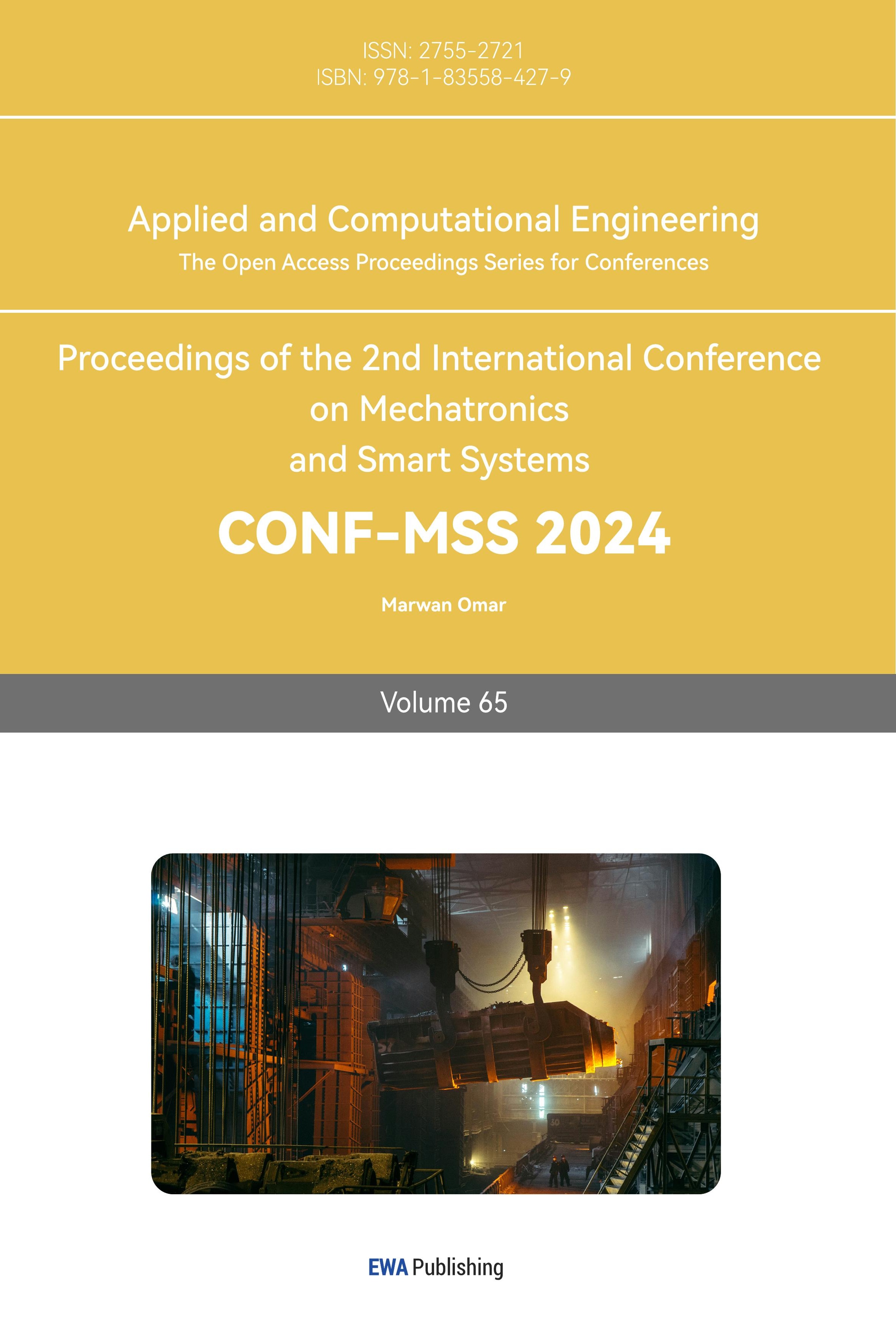
According to different conductive methods Metal-Oxide-Semiconductor Field-Effect Transistor (MOSFET) can be classified into Enhancement MOS and Depletion MOS. For each class of MOSFET, they can be classified into PMOS and NMOS. The N-channel enhanced MOSFET is basically a left-right symmetric topology structure.
It generates a layer of SiO2 thin film insulation layer on a P-type semiconductor, and then diffuses two highly doped N-type regions using photolithography technology, leading out the electrodes from the N-type region, one is the drain electrode D and the other is the source electrode S. A layer of metal aluminium is plated on the insulation layer between the source and drain electrodes as the gate G. An ohmic contact electrode is connected to the substrate and is called substrate electrode. The diagrammatic sketch is shown in Figure 1 [4].
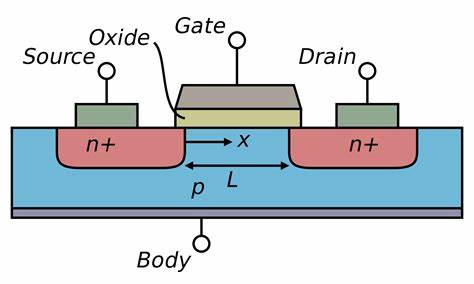
Figure 1. diagrammatic sketch of MOSFET [4]
When the voltage between gate and source ( \( {V_{GS}} \) ) is 0. The P-type semiconductor and the two regions diffused with N-type semiconductor can be regarded as 2 diodes that are connected back to back, which means there will be no current through the device.
When \( {V_{GS}} \) is higher than 0, for the source of the NMOS is connected to the substrate, there will be an electric field from gate to substrate. With the effect from electric field, the multi carrier holes in the P-type semiconductor near the gate are repelled downwards, resulting in a thin depletion layer of electrons. But when the voltage between gate and source is not big enough, the number of electrons between drain and source is not going to be big enough to form a current channel, which means the \( {V_{GS}} \) will keep 0.
When \( {V_{GS}} \) continue to increase to the threshold voltage ( \( {V_{TH}} \) ), most of the holes on the surface of the P-type semiconductor will be repelled and the amount of the electrons will be enough to change the surface of the P substrate into N-type layer, known as the “inverted layer”, and form a current channel between drain and source [4]. As shown in the figure 2.
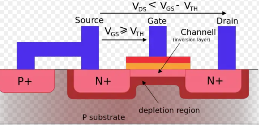
Figure 2. Inverter layer (Photo/Picture credit: Original)
The larger the \( {V_{GS}} \) , the thicker the channel. In that case, when there is a voltage between drain and source ( \( {V_{DS}} \) ), there will be current from drain to source.
For the resistance in the channel, the voltage drop exists. Gradually reduce the potential of each point in the channel from the source to the drain along the channel. The voltage in the drain is the smallest, which means the channel near the drain is the thinnest. In that case, the thickness of the channel is no longer uniform, and the entire channel is inclined. With the growth of the \( {V_{DS}} \) the channel near the drain will become thinner, and when it comes to a critical point.
\( {V_{DS}}={V_{GS}}-{V_{T}} \ \ \ (1) \)
The channel at the drain end disappears, leaving only the depletion layer, which is called “pre pinch off”. As shown in the figure 3.
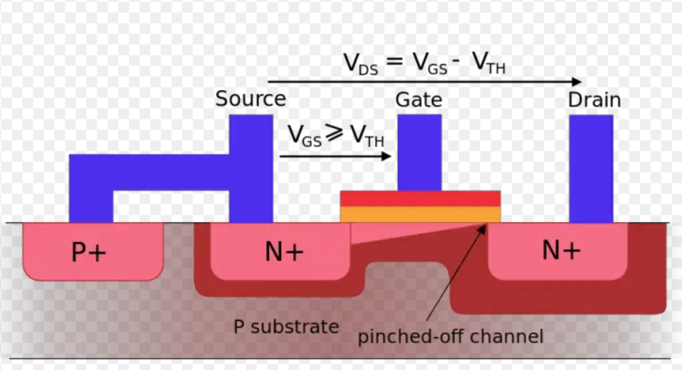
Figure 3. Pre pinch off (Photo/Picture credit: Original)
When \( {V_{DS}} \) keep growing, the pinch off point will keep moving from drain to source. As shown in figure 4.
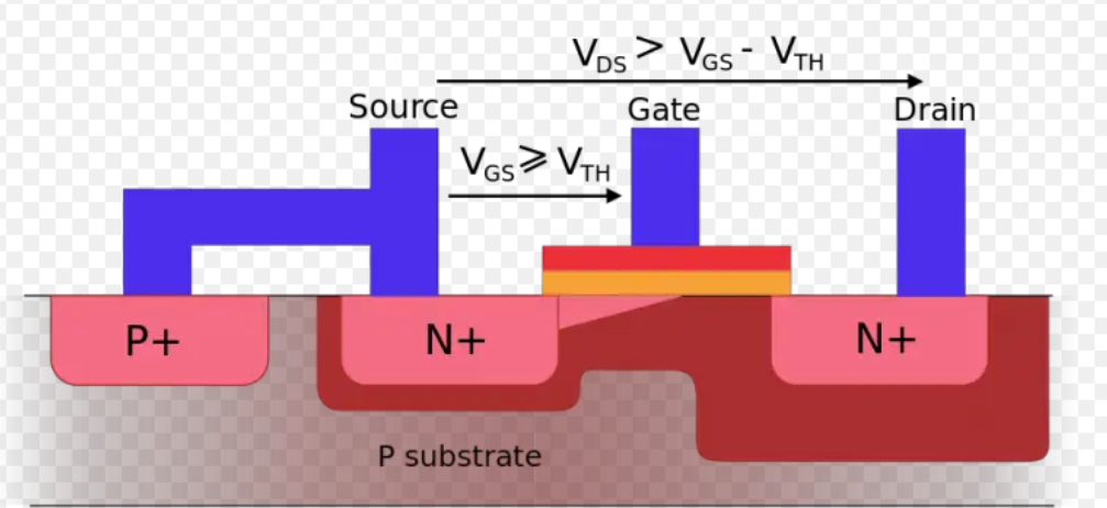
Figure 4. Moving of pinch off point (Photo/Picture credit: Original)
In that case, when \( {V_{DS}} \) keep growing, the drain current will no longer grow. The characteristic curves are shown in the following figure 5.
|
|
(a) | (b) |
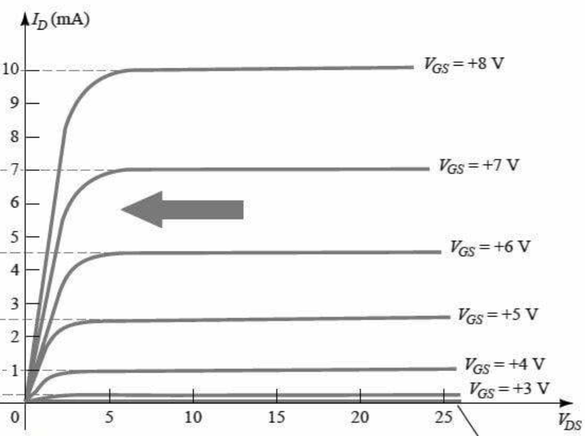
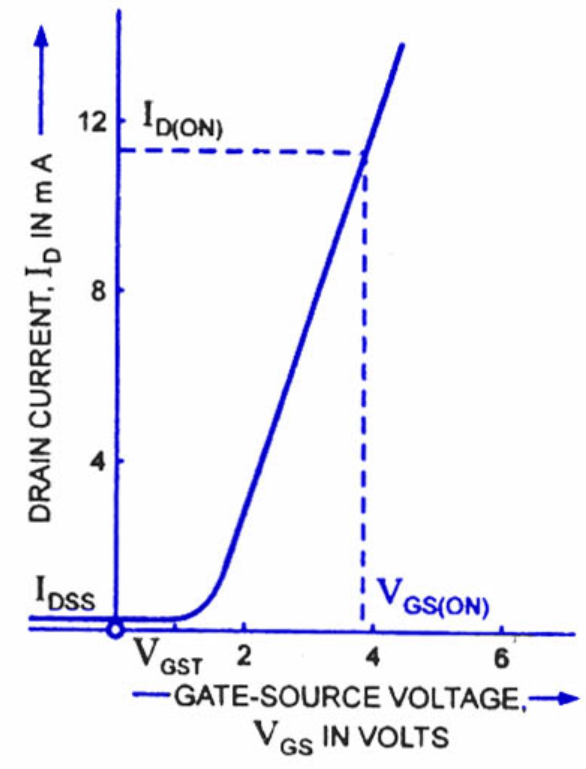
Figure 5. Work curves (Photo/Picture credit: Original)
The Enhancement PMOS is quite similar to NMOS, but the direction of current and voltage are opposite to NMOS.
The structure of Depletion MOS is similar to Enhancement MOS, but positive ions are implanted previously in its SiO2 insulation layer so that when \( {V_{GS}} \) is 0, the positive ions can still form an electric field from gate to substrate which attract enough electrons to form a channel from drain to source. When \( {V_{GS}} \) get lower than 0, the electric field will be
Weakened which make the channel thinner and reduce the current. When it comes to pinch off voltage \( {V_{P}} \) , the current will be 0. The characteristic curve is shown in the following figure 6.
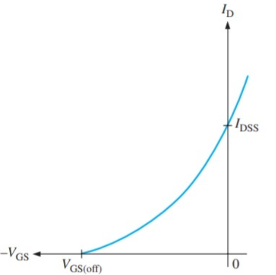
Figure 6. Work curve of Depletion MOS (Photo/Picture credit: Original)
2.2. Structure of GaN HEMT and its working principle
Structurally, GaN High electron mobility transistor9(HEMT) can be classified into horizontal structure and longitudinal structure. According to different conductive methods, it can be classified into normal on GaN HEMT and normal off GaN HEMT. The basic structure of a typical normal on GaN HEMT is shown in figure 7 [5].
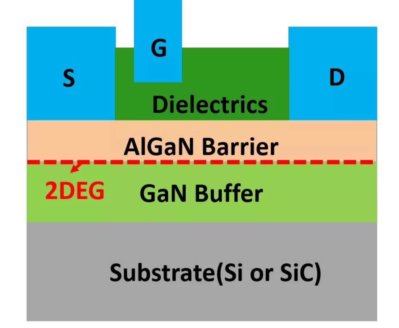
Figure 7. Structure of GaN HEMT [4]
The bottom layer of the device is the substrate layer, followed by the epitaxial growth of an N-type GaN buffer layer and the epitaxial growth of a P-type AlGaN barrier layer, forming an AlGaN/GaN heterojunction. Finally, the gate electrode is deposited on the AlGaN layer, and the source electrode and drain electrode are heavily doped and connected to the two-dimensional electron gas in the channel to form an ohmic contact.
In the GaN, there is huge Electronegativity difference between Ga and N, so that the N-GA covalent bond has strong polarization characteristics. The wurtzite structure of GaN is non centrosymmetric, and its covalent bond in the vertical direction is longer, so that it has spontaneous polarization phenomenon. For the lattice constant of GaN is larger than AlGaN, the GaN will give the AlGaN an outward stress, which cause the Piezoelectric polarization in AlGaN. For the AlGaN layer is much thinner than GaN, the stress given by AlGaN can be ignored. Totally, in AlGaN layer there is Piezoelectric polarization and spontaneous polarization, and in GaN layer there is only spontaneous polarization. So the electric field from up to down in AlGaN is stronger than GaN, so that the interface between two materials has positive charge. And the is band order difference between the energy bands of two materials. When they form the heterojunction, they have to rebalance the energy bands in order to make the Fermi energy levels equal. And the energy band of conduction band edge will bend, and that make it smaller than the Fermi energy level, which build a quantum well that collect many electrons. At the same time, the high potential barrier on one side of the wide bandgap AlGaN makes it difficult for electrons to cross the potential well, and electrons are restricted from moving laterally in the thin layer at the interface, which is called two-dimensional electron gas (2DEG) [4].
\( {V_{DS}} \) can build a lateral electric field, which activates 2DEG to form \( {i_{d}} \) . And \( {V_{GS}} \) can control the deepness of the quantum well which change the size of the two-dimensional electron gas surface density in the channel to control \( {i_{d}} \) . For normal on GaN HEMT, when \( {V_{GS}} \) is 0, 2DEG already exist. When \( {V_{GS}} \) is lower than 0, it will form a reverse electric field and cut off 2DEG. For normal off GaN HEMT, only when \( {V_{GS}} \) is higher than 0, the 2DEG exist. In that case, the working curves of HEMT are almost consistent with those of MOSFET.
3. The applications of MOSFET and HEMT
3.1. The advantages of MOSFET and its application
MOSFETs (Metal-Oxide-Semiconductor Field-Effect Transistors) exhibit several advantages including high input impedance, minimal on-resistance, rapid switching capabilities, absence of secondary breakdown, and a reduced noise figure. Traditionally, silicon (Si) has been the primary material for MOSFETs. However, recent advancements have seen the adoption of Silicon Carbide (SiC) in high-voltage power conversion applications due to its superior performance attributes.
Hai Xu critically examines and contrasts two MOSFET models: Cree’s second-generation SiC MOSFET (C2M0080120D) and IXYS’s Si MOSFET (IXFH24N90P) [6]. Experimental analysis reveals that SiC MOSFETs demonstrate lower on-resistance, indicating reduced power loss, alongside a decreased threshold voltage and augmented breakdown voltage, thereby enhancing blocking performance. These findings suggest that SiC effectively optimizes the inherent advantages of MOSFETs in terms of conduction resistance and stability.
In contemporary applications, SiC MOSFETs have become prevalent in switching devices due to their high operating junction temperature, elevated breakdown voltage, increased power density, higher switching frequency, and reduced switching power loss [7]. An illustrative example is a MOSFET-based bidirectional switching power pole (BSPP), which benefits from SiC MOSFETs through a power trace design that minimizes parasitic inductance and balances transient performance between high-side and low-side power MOSFETs, achieving optimal switching performance.
Beyond switching devices, MOSFETs are integral to power amplifiers, where cost-effectiveness, low distortion, and interference resistance are critical. While traditional Class AB amplifiers exhibit low efficiency, SiC MOSFETs are increasingly applied to Class B amplifiers. This study introduces an enhanced Baxandall quasi-complementary output circuit using SiC, complemented by auxiliary circuits such as output current detectors and BUCK topology control circuits. Simulation results indicate a maximum undistorted power output of 251.17W for the amplifier, with an efficiency improvement of 26% post-optimization [8].
3.2. The advantages of HEMT and its application
Power electronic devices, traditionally operated at standard ambient temperatures, acquire critical importance in specialized fields like aerospace and superconductivity where their performance in cryogenic environments is vital.
Chenyu Tian investigates key electrical parameters — threshold voltage, breakdown voltage, and on-resistance — of SiC MOSFETs and GaN HEMTs under low-temperature conditions (ranging from 300K to 77K) [9]. The baseline characteristics of the SiC MOSFET include a threshold voltage of 4V, breakdown voltage of 1200V, and on-resistance of 160Ω, while the GaN HEMT exhibits a threshold voltage of 1.4V, breakdown voltage of 600V, and on-resistance of 93.5Ω. At reduced temperatures, the SiC MOSFET displayed an increase in threshold voltage from 2.707V to 7.505V, a decrease in breakdown voltage from 1610.4V to 1079.2V, and an increase in on-resistance from 0.223Ω to 2.775Ω. The contrasting trends observed between the two components are attributed to their distinct structural properties. The study concludes that GaN HEMTs demonstrate superior electrical properties in low-temperature environments compared to SiC MOSFETs.
Further, the potential of GaN HEMTs in space exploration is explored. These devices are considered for use in communication and navigation satellites, where they could replace traveling wave tube amplifiers (TWTA) commonly used for their high output power capability above the L-band [10]. Despite a lower maximum output power compared to MOSFETs, GaN HEMTs offer advantages in terms of weight, size, and performance efficiency. The study involved testing the output power, linear gain, power increase efficiency of HEMTs in the L/S band, and designing a hybrid microwave integrated circuit with two-stage HEMT to optimize weight and size while enhancing efficiency. The device’s applicability in the S-band and its stability in various radiation environments were verified through DC High Temperature Operating Life Test (DC HTOL) and RF High Temperature Operating Life Test (RF HTOL), affirming its feasibility in space environments.
Finally, the paper discusses the prospects of GaN HEMTs in ultra high-speed wireless communication, high-sensitivity sensing, and imaging in millimeter-wave and terahertz-wave wireless communication within the domains of 5G and future-generation mobile communication systems. The exceptional electrical characteristics of GaN HEMTs, including a high current gain cutoff frequency (fT) reaching 450GHz and a maximum oscillation frequency (fmax) of 600GHz, underscore their potential in advancing wireless communication technology [11].
3.3. Comparison between HEMT and MOSFET
HEMT and MOSFET are both high-performance electronic components. The advantages of MOSFET lies in its fast switch speed, good stability, and its lower costs. It can be used in logic circuit, signal amplifier, and electric switching. His biggest problem is performance issues in ultra-high pressure and ultra-high temperature environments.
Although the SiC MOSFET solved the problem of high-pressure environment, the working condition in extreme temperature environments is still not ideal. Due to its unique 2DEG, GaN HEMT performs better in low-temperature environments than MOSFET. Its excellent output power, radiation resistance, and low quality make it have great prospects in the field of communication satellites, and space exploration. However, due to its high cost, its widespread application still faces certain difficulties. This table 1 represents the commonalities and differences between MOSFET and HEMT.
Table 1. Comparison between HEMT and MOSFET
MOSFET | HEMT | |
Commonalities | Fast switching speed, good stability | |
Advantage | Low cost, no secondary breakdown, low noise figure | Good performance in high-pressure and high-temperature environments |
Disadvantage | Poor performance in high-pressure and high-temperature environments | Expensive raw materials, high costs |
4. Conclusion
Based on the analysis above, the conclusion drawn in this article is as follows: both MOSFET and HEMT have gate, drain, source, and body structures. But there are significant differences in their conductive mechanisms. MOSFET mainly relies on the inversion layer formed by the upward shift of electrons caused by the voltage between the gate and source for conduction. HEMT mainly relies on the 2deg formed between the gate and drain due to material and other factors for conductivity. Although the two have different guiding principles, their working curves are relatively similar. MOSFET and HEMT are both high-performance semiconductor devices, with advantages such as good stability and fast switching speed. The unique advantage of MOSFET lies in its relatively mature production process and material cost, while HEMT has excellent advantages such as anti-interference, radiation resistance, and high temperature resistance. However, HEMT is relatively difficult to manufacture and has high costs.MOSFET is often used in circuit conversion switches and high-power amplifiers, while HEMT can be used in fields such as chargers and even satellites.
Semiconductor materials are the most important electrical materials in various fields in the 21st century, and their development is related to the progress of the world in high-tech industries. The main difficulties in the development of semiconductor materials are precision, integration, and production processes. The production process difficulties include single point production and batch production. At present, the number of transistors integrated on the chip has reached billions, and the precision of transistors has reached the nanometer level. With the continuous improvement of integration and precision, further technological development will inevitably become more difficult. The efficient parallel connection of multiple HEMTs and the reduction of energy loss are also worthy of research. The simulation models of SiC MOSFET and GaN HEMT have a significant impact on the reliability of their circuits. However, with the increasing demand for semiconductor materials, it is believed that investment in semiconductor technology breakthroughs will also continue to increase. The development of semiconductor technology will definitely have a decisive role in the development of all industries of humanity.
The demand for semiconductor materials in various industries around the world will definitely increase in the future. Semiconductor materials with more complex processes and better effects will definitely be created and applied with the advancement of human technology. This article only explores two widely used semiconductor materials, MOSFET and HEMT.
References
[1]. Al-bayati, Ali MS, et al. “A comparative design and performance study of a non-isolated DC-DC buck converter based on Si-MOSFET/Si-Diode, SiC-JFET/SiC-schottky diode, and GaN-transistor/SiC-Schottky diode power devices.” 2017 North American power symposium (NAPS). IEEE, 2017.
[2]. Kanale A, Baliga B J. Comparison of current suppression methods to enhance short circuit capability of 1.2 kV SiC power MOSFETs: A new approach using a series-connected, gate-source-shorted Si depletion-mode MOSFET vs reduced gate bias operation. IECON 2019-45th Annual Conference of the IEEE Industrial Electronics Society. IEEE, 2019, 1: 5114-5119.
[3]. Chen J, Hua M, Wang C, et al. Decoupling of forward and reverse turn-on threshold voltages in Schottky-type p-GaN gate HEMTs. IEEE Electron Device Letters, 2021, 42(7): 986-989.
[4]. Lu J, Hou R, Chen D. Loss distribution among paralleled GaN HEMTs. 2018 IEEE Energy Conversion Congress and Exposition (ECCE). IEEE, 2018: 1914-1919.
[5]. Tsukamoto H, Shintani M, Sato T. A study on statistical parameter modeling of power MOSFET model by principal component analysis. 2019 IEEE 32nd International Conference on Microelectronic Test Structures (ICMTS). IEEE, 2019: 107-112.
[6]. Hai Xu; Xiangyang Liu; Sen cao; Guoguang Li. Design of resonant converter based on silicon carbide devices and their drivers. power electronic technology, 2023,57(10):127-129+136.
[7]. Sayed H, Zurfi A, Zhang J. Design and experiments of a SiC power MOSFET bidirectional switching power pole. 2016 IEEE 25th International Symposium on Industrial Electronics (ISIE). IEEE, 2016: 460-464.
[8]. Weiheng Liu. Design of a Low Frequency Linear Power Amplifier Driven by SiC MOSFET. University of Electronic Science and technology, 2020.
[9]. Chenyu Tian; Wenyong Guo; Chuang Zhao; Wenju Sang; Suhang Yu. Low temperature characteristics testing and comparative analysis of SiC MOSFET and GaN HEMT. Cryogenics and Superconductivity,2022,50(07):39-43+76.
[10]. Satoh T, Osawa K, Nitta A. GaN HEMT for space applications. 2018 IEEE BiCMOS and Compound Semiconductor Integrated Circuits and Technology Symposium (BCICTS). IEEE, 2018: 136-139.
[11]. Watanabe I, Yamashita Y, Kasamatsu A. Research and development of GaN-based HEMTs for millimeter-and terahertz-wave wireless communications. 2020 IEEE International Symposium on Radio-Frequency Integration Technology (RFIT). IEEE, 2020: 19-21.
Cite this article
Li,Y. (2024). Comparative analysis of working principles and applications of MOSFET and HEMT. Applied and Computational Engineering,65,66-74.
Data availability
The datasets used and/or analyzed during the current study will be available from the authors upon reasonable request.
Disclaimer/Publisher's Note
The statements, opinions and data contained in all publications are solely those of the individual author(s) and contributor(s) and not of EWA Publishing and/or the editor(s). EWA Publishing and/or the editor(s) disclaim responsibility for any injury to people or property resulting from any ideas, methods, instructions or products referred to in the content.
About volume
Volume title: Proceedings of Urban Intelligence: Machine Learning in Smart City Solutions - CONFSEML 2024
© 2024 by the author(s). Licensee EWA Publishing, Oxford, UK. This article is an open access article distributed under the terms and
conditions of the Creative Commons Attribution (CC BY) license. Authors who
publish this series agree to the following terms:
1. Authors retain copyright and grant the series right of first publication with the work simultaneously licensed under a Creative Commons
Attribution License that allows others to share the work with an acknowledgment of the work's authorship and initial publication in this
series.
2. Authors are able to enter into separate, additional contractual arrangements for the non-exclusive distribution of the series's published
version of the work (e.g., post it to an institutional repository or publish it in a book), with an acknowledgment of its initial
publication in this series.
3. Authors are permitted and encouraged to post their work online (e.g., in institutional repositories or on their website) prior to and
during the submission process, as it can lead to productive exchanges, as well as earlier and greater citation of published work (See
Open access policy for details).
References
[1]. Al-bayati, Ali MS, et al. “A comparative design and performance study of a non-isolated DC-DC buck converter based on Si-MOSFET/Si-Diode, SiC-JFET/SiC-schottky diode, and GaN-transistor/SiC-Schottky diode power devices.” 2017 North American power symposium (NAPS). IEEE, 2017.
[2]. Kanale A, Baliga B J. Comparison of current suppression methods to enhance short circuit capability of 1.2 kV SiC power MOSFETs: A new approach using a series-connected, gate-source-shorted Si depletion-mode MOSFET vs reduced gate bias operation. IECON 2019-45th Annual Conference of the IEEE Industrial Electronics Society. IEEE, 2019, 1: 5114-5119.
[3]. Chen J, Hua M, Wang C, et al. Decoupling of forward and reverse turn-on threshold voltages in Schottky-type p-GaN gate HEMTs. IEEE Electron Device Letters, 2021, 42(7): 986-989.
[4]. Lu J, Hou R, Chen D. Loss distribution among paralleled GaN HEMTs. 2018 IEEE Energy Conversion Congress and Exposition (ECCE). IEEE, 2018: 1914-1919.
[5]. Tsukamoto H, Shintani M, Sato T. A study on statistical parameter modeling of power MOSFET model by principal component analysis. 2019 IEEE 32nd International Conference on Microelectronic Test Structures (ICMTS). IEEE, 2019: 107-112.
[6]. Hai Xu; Xiangyang Liu; Sen cao; Guoguang Li. Design of resonant converter based on silicon carbide devices and their drivers. power electronic technology, 2023,57(10):127-129+136.
[7]. Sayed H, Zurfi A, Zhang J. Design and experiments of a SiC power MOSFET bidirectional switching power pole. 2016 IEEE 25th International Symposium on Industrial Electronics (ISIE). IEEE, 2016: 460-464.
[8]. Weiheng Liu. Design of a Low Frequency Linear Power Amplifier Driven by SiC MOSFET. University of Electronic Science and technology, 2020.
[9]. Chenyu Tian; Wenyong Guo; Chuang Zhao; Wenju Sang; Suhang Yu. Low temperature characteristics testing and comparative analysis of SiC MOSFET and GaN HEMT. Cryogenics and Superconductivity,2022,50(07):39-43+76.
[10]. Satoh T, Osawa K, Nitta A. GaN HEMT for space applications. 2018 IEEE BiCMOS and Compound Semiconductor Integrated Circuits and Technology Symposium (BCICTS). IEEE, 2018: 136-139.
[11]. Watanabe I, Yamashita Y, Kasamatsu A. Research and development of GaN-based HEMTs for millimeter-and terahertz-wave wireless communications. 2020 IEEE International Symposium on Radio-Frequency Integration Technology (RFIT). IEEE, 2020: 19-21.