


1. Introduction
Uninterruptible Power Supply (UPS), is a kind of power protection equipment containing energy storage device, inverter as the main unit, voltage stabilization and frequency stabilization output [1]. UPS has three major features of voltage stabilization, filtering and uninterruptibility. When the utility power is normal, the UPS will utility voltage stabilization for load use, while charging the battery; once the utility power is abnormal. Such as blackout, over-voltage under-voltage, UPS immediately release the electrical energy in the battery, the output voltage to the outside, so that the load works normally and is protected. Therefore, the UPS can supply uninterrupted, safe and stable power to the power equipment, and is now widely used in the electronic information industry, aerospace and many other fields.
2. Main circuit design
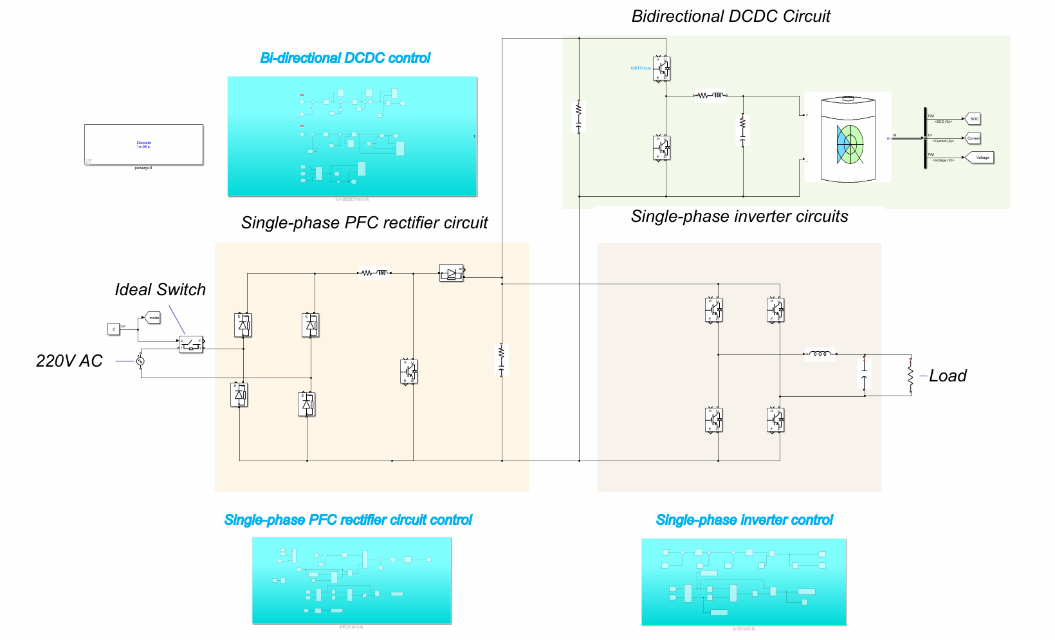
The single-phase on-line interactive uninterruptible power supply (UPS), as shown in Figure. 1, consists of three parts: a power factor correction circuit, an inverter circuit and a bidirectional DC/DC circuit.
The uninterruptible power supply system consists of two working modes: normal operation and energy storage power supply. When the system is in normal operation, i.e., the utility power can be supplied normally, 220V AC power is rectified to DC through the power factor correction circuit, and the DC is supplied to the load through the inverter circuit, and at the same time, the DC is supplied to the battery through the bi-directional DC/DC circuit; when the system is in the storage power supply, i.e., the utility power is abnormal, the battery is discharged, and the power is supplied to the load through the bi-directional DC/DC circuit and the inverter circuit. Therefore, the uninterruptible power supply system can ensure uninterrupted and stable operation of the load.
|
Figure 1. Simulation circuit diagram of uninterruptible power supply system |
2.1. Fundamental principle
2.1.1. Power Factor Correction Circuit. To reduce the pollution of the grid by harmonic currents and to improve the power quality, the power factor needs to be improved [2]. In circuits containing nonlinear devices such as diodes, the power factor (PF) is often calculated using equation (1):
\( PF=\frac{P}{S}=\frac{{U_{1}}{I_{1}}cos{{φ_{1}}}}{UI} \) (1)
Where \( {U_{1}},{I_{1}} \) for the input voltage, current base wave RMS, respectively, respectively \( U,I \) for the AC voltage, current RMS, \( {φ_{1}}{φ_{1}} \) for the phase difference between the base wave voltage and base wave current.Since the grid voltage distortion rate is small, \( {U_{1}}=U \) , it can be obtained by combining the definition of total harmonic distortion rate (THD):
\( PF=ξcos{{φ_{1}}}=\frac{1}{\sqrt[]{1+TH{D^{2}}}}cos{{φ_{1}}} \) (2)
From equation (2), it can be seen that to improve the power quality and power factor, it is necessary to reduce the distortion rate of the current, and at the same time correct the phase of the voltage and current. In this paper, single-phase PFC Boost is used as the power factor correction circuit, when the utility power is normal, the AC power is rectified and stabilized by the Boost circuit to boost the voltage, and then through the control strategy to make the input voltage and current present sinusoidal waveforms with the same phase change, to achieve the function; when the utility power is abnormal, the single-phase PFC Boost circuit does not work.
2.1.2. Inverter circuit. Inverter is a way of transforming and controlling electrical energy, which converts direct current into alternating current. In this paper voltage source type full bridge inverter circuit is used.
2.1.3. Bidirectional DC/DC Circuit. Bidirectional DC/DC converter circuit can realize bidirectional voltage increase and decrease, the module has two working modes, respectively, Buck (battery charging) and Boost (battery discharging), when the circuit is in the Buck mode, when the utility power is normal to supply power for the load, and at the same time charging the battery; when it is in the Boost mode, the utility power is abnormal, and the battery is discharged.
2.2. Circuit Parameter Design
The simulation model of the UPS system is built, the topology is shown in Figure. 1 and the system parameters are shown in Table 1.
Table 1. System parameters
Name | Symbols | Numerical value |
Rated output power | Po | 20kW |
Rated Input Voltage | U | 220V |
Grid frequency | f | 50Hz |
Switching frequency | fs | 20kHz |
DC bus voltage | Ubus | 600V |
Battery bank voltage | Ubat | 400V |
2.2.1. Power Factor Correction Circuit. For the inductor value of the power factor correction circuit, the inductor current ripple coefficient is generally taken to be 0.2, so the inductor value is satisfied:
\( L≥\frac{5{U_{dc}}{U_{max}}}{8{f_{s}}{P_{o}}} \) (3)
Where \( {U_{max}} \) is the peak value of the frontal input voltage. The inductance value \( L≥291.56μH \) is calculated according to equation (3), so the inductance is set to \( 300μH \) in the simulation circuit.
For the filter capacitance, the maximum ripple peak value is less than 3%, and the permissible voltage fluctuation \( ΔU \) is within 18V, the output side capacitance value formula can be obtained.
\( C≥\frac{{P_{o}}}{2ωΔU{U_{o}}} \) (4)
Substituting the parameters gives \( C≥2.9mF \) , setting the capacitance \( C=3mF \) in the simulated circuit.
2.2.2. Inverter Circuit. The inductance and capacitance of the inverter circuit can affect the waveform of the output voltage, and the filter inductance is calculated as [3]:
\( L=\frac{{U_{dc}}{T_{si}}}{8{λ_{L}}{I_{rms}}} \) (5)
In the above equation \( {T_{si}}=\frac{1}{{f_{si}}} \) , \( {I_{rms}} \) are the effective values of the output current of the inverter circuit. Considering \( {λ_{L}}≤20\% \) , yields the inductance \( L≥206.25μH \) and hence \( L=300μH \) is chosen.
In the capacitance design, it is considered that at the fundamental frequency, the filter capacitor absorbs reactive power less than 5% of the active power of the system. Therefore the maximum value of filter capacitance is obtained:
\( {C\frac{0.05{P_{o}}}{2π{f_{o}}U_{c}^{2}}_{max}} \) (6)
Where \( {U_{c}} \) is the voltage across the filter capacitor and \( {f_{o}} \) is the rated frequency. The maximum value of the filter capacitor is \( 65.77μF \) , and \( 50μF \) is selected for this simulation.
2.2.3. Bidirectional DC/DC Circuit. The UPS system designed in this paper has the current in continuous mode of operation (CCM). When in Buck mode, the duty cycle DBuck=2/3 at this time, in addition to the inductor current and voltage ripple need to be less than 6%, so the inductor and capacitor in this mode can be obtained [4]:
\( \begin{cases} \begin{array}{c} L≥\frac{{U_{bus}}{D_{Buck}}(1-{D_{Buck}})}{Δ{i_{L}}{f_{s}}}=2.2mH \\ C≥\frac{1-{D_{Buck}}}{8Lf_{s}^{2}×2\%}=2.367uF \end{array} \end{cases} \) (7)
When in Boost mode, the minimum load power is specified to be 1/10 of the rated power and it is assumed that there is no power loss, so the inductance is satisfied:
\( L≥\frac{{U_{bus}}}{2{Is_{bat-min}}{{{D_{Boost}}_{Boost}}^{2}}} \) (8)
For the DC bus-side equivalent resistance \( R=\frac{U_{bus}^{2}}{P}=18Ω \) , the bus-side capacitance is therefore obtained:
\( {C_{dc}}≥\frac{{D_{Boost}}}{0.02R{f_{s}}}=463μF \) (9)
In summary, since the bidirectional DCDC has two modes, the inductance needs to be full of both Equation. (7) and Equation. (8), so the inductance parameter is selected as 2.21 mH, the battery-side capacitance parameter is 10.5 mF, and the dc bus-side parameter is 0.12 F in the simulation.
3. Control strategy analysis
In order to further provide stable and uninterrupted power to the load, the three main circuits in the UPS system designed in this paper correspond to three control modules, and their control principles are shown in Figure. 2.
|
Figure 2. UPS system overall control block diagram |
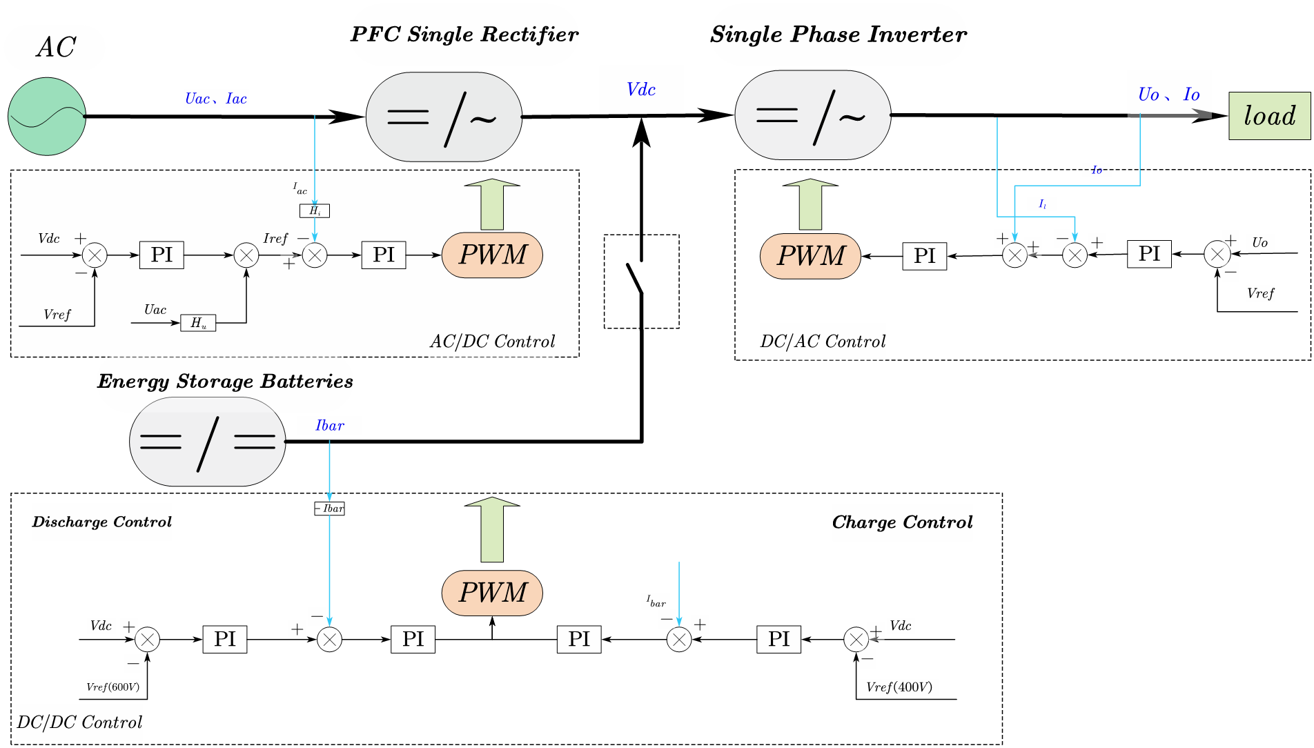
3.0.1. Power factor correction circuit control. The single-phase power factor correction circuit control link adopts a double closed-loop structure, with the outer ring being the voltage ring and the inner ring being the inductor current ring. The outer loop compares the output voltage ring with the reference voltage 600V, calculates the quotient of the input voltage divided by the peak value of the AC grid, and the voltage ring is multiplied by the PI regulator with the quotient value as the reference value of the current ring to realize that the output voltage is constant with the given voltage; the inner loop compares the inductor current with the above reference value of the current, and then, after the adjustment of the PI regulator, generates a pulse signal to control the on-off of the IGBTs by means of the PWM pulse generator module, which realizes the inductance current control of the IGBTs and the inductance current control of the inductor. The inner loop compares the inductor current with the above current reference value and then generates the pulse signal to control the on-off of IGBT through the PWM pulse generator module to realize the in-phase operation of voltage and current. After simulation, the PI parameters of the voltage loop are P=15,1=90, and the PI parameters of the current loop are P=500, I=1.
3.0.2. Single-phase inverter circuit control. The single-phase inverter circuit control link has a double closed-loop structure, with the outer loop being the voltage loop and the inner loop being the current loop. The outer loop compares the output voltage with the set ideal sinusoidal waveform, calculates the difference between the inductor current and the load current, and adds the outer voltage loop to this difference through the PI regulator, and takes this difference as the reference value of the inner loop, which is regulated by the PI regulator of the inner loop through the PWM pulse generator module to produce two complementary control signals. After simulation adjustment, the PI parameters of the outer loop can be obtained as P=1, I=250; the PI parameters of the inner loop are P=27.066, I=6.67.
3.0.3. Bidirectional DC/DC converter control. The bidirectional DCIDC control link is divided into two parts, charging control and discharging control, which specifies that the inductor current reference is positive when the battery is charging and negative when discharging [5]. Both the charging control link and the discharging control link use a double closed-loop structure, and the difference between the two is that the reference value of the outer voltage loop is different. When the circuit is in the charging link, the reference voltage is the rated voltage of the battery pack 400 V. When the circuit is in the discharging link, the reference voltage is the bus voltage 600 V. However, the inner loop of both control modes is the current loop, which ultimately generates the control signals through the PWM pulse module. After simulation adjustment, the PI parameters of the outer ring of the charging control link are: P=100, I=200; the PI parameters of the inner ring are: P=1,1=0.5, the PI parameters of the outer ring of the discharging control link are: P=0.0001,I=8:the PI parameters of the inner ring are: P=0.002.I=0.008.
4. Performance analysis
4.1. Circuit Parameter Design
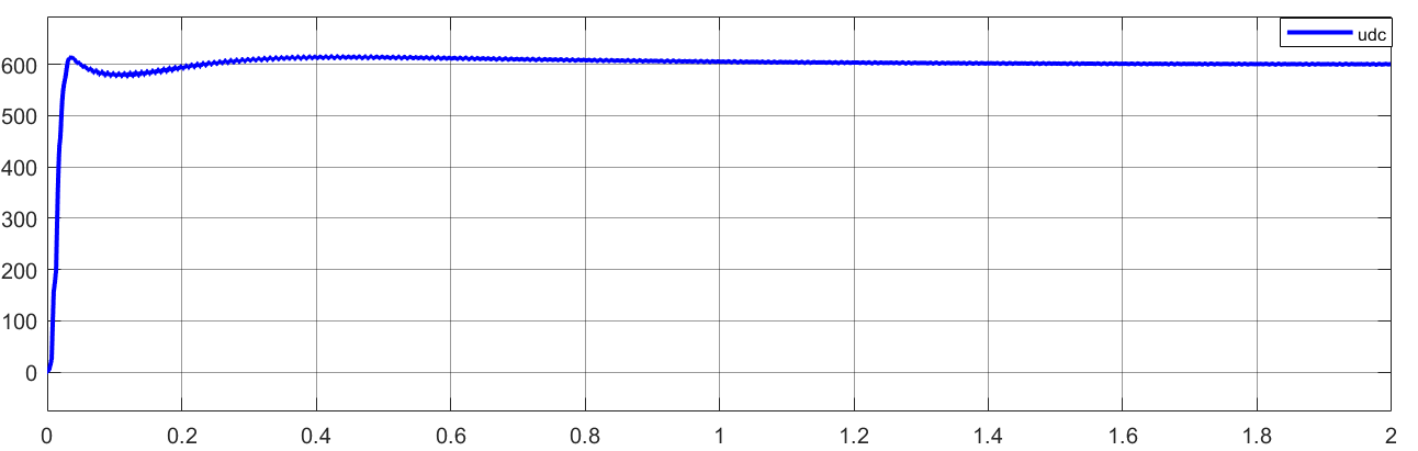
When the utility power is normal, 200V AC is rectified by the power factor correction circuit to output 600V DC, and the voltage waveform is shown in Figure 3.
|
|
Figure 3. PFC output voltage | Figure 4. Diagram of rectifier voltage and inductor current |
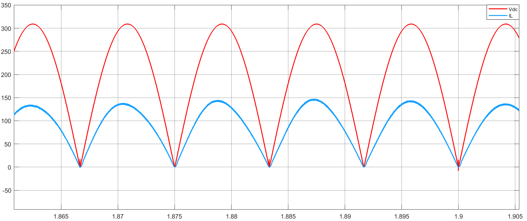
After the system enters the steady state, the current harmonic distortion rate THD of the power factor correction circuit is 2.58%, and the power factor is about 0.966. The output voltage of the rectifier part of the circuit and the waveform of the inductor current are shown in Figure. 4, which indicates that at this time, the voltage and the current are in the same phase, and it achieves the purpose of correcting the power factor and improving the quality of power.
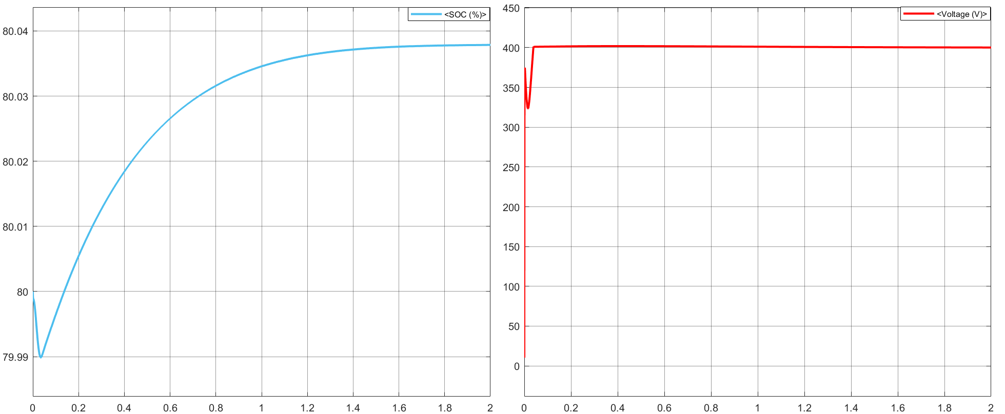
Set the initial battery voltage of 380V, the initial capacity of 80%, at this time the PFC electrical output of 600V DC through the bi-directional DC/DC Buck circuit to the battery charging, battery SOC curves and terminal voltage image in Figure 5 and Figure 6.
|
| |
Figure 5. Battery SOC curve (charging) | Figure 6. Terminal voltage (charging) |

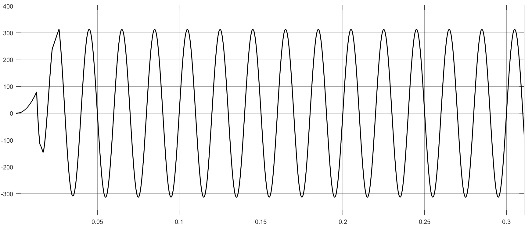
The 600V DC output from the PFC is converted to 220V AC by the inverter circuit to supply power to the load, and the waveform of the voltage at both ends of the load is shown in Figure. 7.
|
| |
Figure 7. Load-side voltage (utility normal) | Figure 8. FFT analysis diagram |
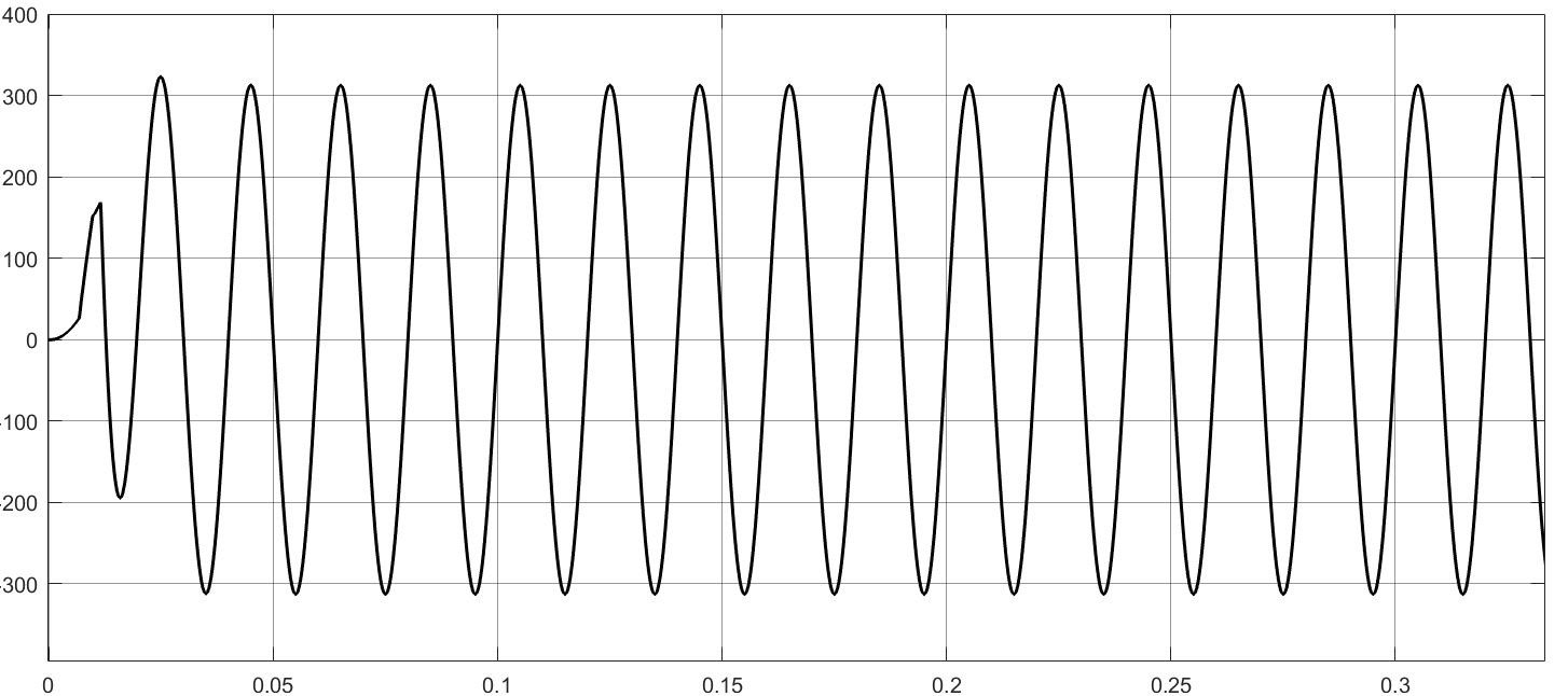
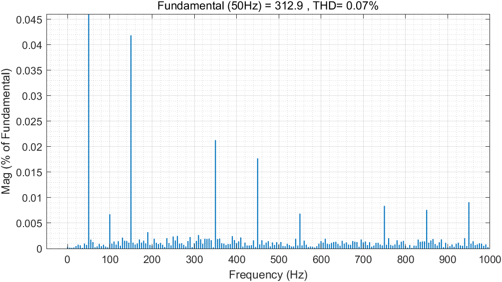
After entering the steady state, the peak value of the load-side voltage is about 311 V. The FFT analysis of the load-side voltage at this time is performed, and the result of FFT analysis is shown in Figure. 8, the total voltage harmonic distortion rate is 0.07%, there is no dc component, and the power factor is 1, which indicates that the sinusoidal degree of the load-side voltage is good.
4.2. Energy Storage Power Mode
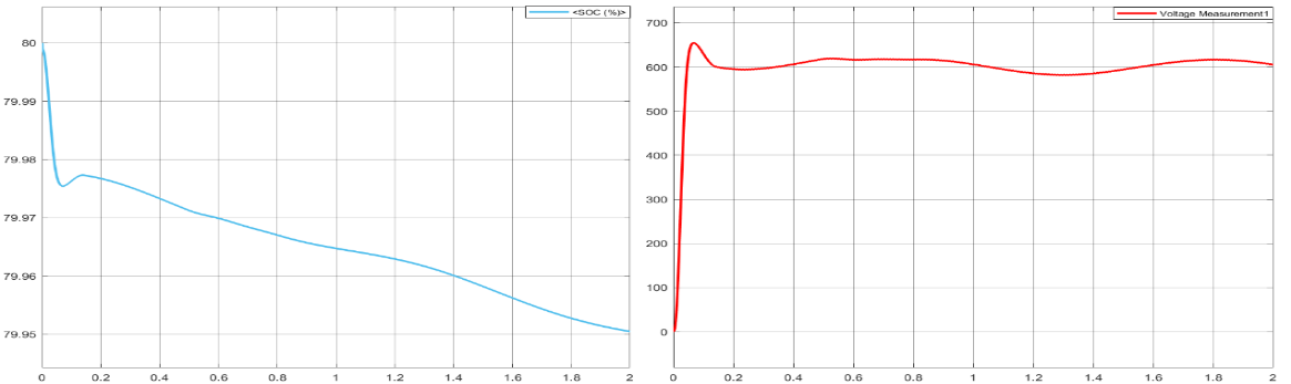
When the utility cannot be normal power supply, 400V battery pack through the bidirectional DC/DC Boost circuit output 600V DC, at this time the battery SOC curve and the output voltage waveform in Figure 9 and Figure 10.
|
| |
Figure 9. Battery SOC curve (discharged) | Figure 10. Busbar voltage (discharged) |

After calculation, the steady-state error of the output voltage of the bidirectional DC/DC circuit is less than 2%, and the inductor current ripple is about 1.7%, which meets the requirements. The 600V DC output from the bidirectional DC/DC goes through the inverter circuit and outputs 220V AC as shown below.
|
Figure 11. Load-side voltage (utility anomaly) |
From the above Figure, it can be seen that when the utility power cannot be supplied normally, the battery pack can be discharged quickly and the adjustment time is short. After entering the steady state, the output AC peak value is about 311V, analyzed by FFT, the total voltage harmonic distortion rate is 0.07%, there is no DC component, and the power factor is 1, which indicates that the load-side voltage waveform is better at this time.
5. Conclusion
In this paper, a single-phase on-line UPS is designed, which contains three parts: single-phase PFC rectifier circuit, inverter circuit and bidirectional DC/DC circuit, focusing on the working principle of each main circuit and control circuit, in addition to analyzing the two modes of operation of the system, and verifying that it is able to provide the loads with continuous and uninterrupted pure sinusoidal alternating current (AC) power, and is therefore usually applied to the environments such as critical computers and important power network equipments.
Acknowledgments
Time flies when a white horse passes, and the writing of this article is nearing its end. From choosing the topic, building the simulation to finalizing the article, it took nearly a month in total. During this period, thanks to all the members, it is our cooperation with each other and not giving up lightly that finally completed this article.
References
[1]. Zhenyuan Dong. Principle and design of single-phase on-line uninterruptible power supply[J]. Electronic Technology and Software Engineering,2021,(10):211-213.
[2]. Xiaolei Song. Improvement and research based on single-phase power factor correction system[D]. Southeast University,2016.
[3]. Suhong Yuan. Design of inverter power supply for vehicle[D]. Beijing Jiaotong University,2019.
[4]. Dongdong Fan. Research on bidirectional DC/DC converter for battery energy storage system[D]. Anhui University of Technology,2017.
[5]. Xvdong Yan . Design and research of a bidirectional DC-DC converter[D]. Nanjing Forestry University,2012.
Cite this article
Xu,Z.;Zhang,Z.;Ren,R.;Wang,W. (2024). Single-phase online interactive uninterruptible power supply design. Applied and Computational Engineering,78,60-66.
Data availability
The datasets used and/or analyzed during the current study will be available from the authors upon reasonable request.
Disclaimer/Publisher's Note
The statements, opinions and data contained in all publications are solely those of the individual author(s) and contributor(s) and not of EWA Publishing and/or the editor(s). EWA Publishing and/or the editor(s) disclaim responsibility for any injury to people or property resulting from any ideas, methods, instructions or products referred to in the content.
About volume
Volume title: Proceedings of the 2nd International Conference on Mechatronics and Smart Systems
© 2024 by the author(s). Licensee EWA Publishing, Oxford, UK. This article is an open access article distributed under the terms and
conditions of the Creative Commons Attribution (CC BY) license. Authors who
publish this series agree to the following terms:
1. Authors retain copyright and grant the series right of first publication with the work simultaneously licensed under a Creative Commons
Attribution License that allows others to share the work with an acknowledgment of the work's authorship and initial publication in this
series.
2. Authors are able to enter into separate, additional contractual arrangements for the non-exclusive distribution of the series's published
version of the work (e.g., post it to an institutional repository or publish it in a book), with an acknowledgment of its initial
publication in this series.
3. Authors are permitted and encouraged to post their work online (e.g., in institutional repositories or on their website) prior to and
during the submission process, as it can lead to productive exchanges, as well as earlier and greater citation of published work (See
Open access policy for details).
References
[1]. Zhenyuan Dong. Principle and design of single-phase on-line uninterruptible power supply[J]. Electronic Technology and Software Engineering,2021,(10):211-213.
[2]. Xiaolei Song. Improvement and research based on single-phase power factor correction system[D]. Southeast University,2016.
[3]. Suhong Yuan. Design of inverter power supply for vehicle[D]. Beijing Jiaotong University,2019.
[4]. Dongdong Fan. Research on bidirectional DC/DC converter for battery energy storage system[D]. Anhui University of Technology,2017.
[5]. Xvdong Yan . Design and research of a bidirectional DC-DC converter[D]. Nanjing Forestry University,2012.