


1. Introduction
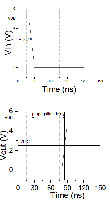
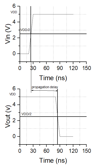
Propagation delay refers to the duration required for a signal to traverse from the input of a circuit or component to its output while undergoing necessary processing or transitions. Propagation delay is a fundamental attribute of electronic circuits and plays a critical role in comprehending the timing and performance of digital circuits. This research specifically aims to investigate the propagation delay in CMOS inverters, which is defined as the duration between when the input changes its logic state halfway ( \( \frac{{V_{dd}}}{2} \) ) and when the output changes its logic state halfway ( \( \frac{{V_{dd}}}{2} \) ) in inverters. Regarding the transmission delay of CMOS inverters, there are two scenarios. In the first scenario, the input of the CMOS inverter transitions from a low voltage level to a high voltage level (rising ramp), while the output transitions from a high voltage level to a low voltage level (falling ramp). In the second scenario, the opposite occurs, where the input of the CMOS inverter transitions from a high voltage level to a low voltage level (falling ramp), and the output transitions from a low voltage level to a high voltage level (rising ramp). The definition of the propagation delay in both scenarios is demonstrated in Fig1 and Fig2. The propagation delay analysis in these two scenarios is symmetric, yielding similar results [1]. Therefore, in the analysis conducted in this paper, we will focus on the case of input transitioning on the rising ramp for discussion.
|
|
Figure 1. Propagation delay of input falling ramp. | Figure 2. Propagation delay of input rising ramp. |
Propagation delay is inevitable due to several factors, such as the input signal propagation delay of the preceding stage, the switch response times of the transistors, and the load capacitance of the subsequent stage circuit. These factors are objectively present and cannot be completely eliminated in the current scientific theory. Therefore, it is impossible to completely eliminate the propagation delay in the CMOS inverter, but it can be reduced to a certain extent through various methods.
Reducing propagation delay is a critical objective in integrated circuit design because it directly impacts the speed at which circuits operate. By minimizing the time required for signals to propagate through inverters, designers can enhance the overall performance and efficiency of CMOS circuits. Faster operation speeds can improve functionality, increase data transfer rates, and enhance system responsiveness, highly desirable in modern electronic devices. Thus, by developing methods to reduce propagation delay, designers can push the boundaries of circuit performance and enable the creation of faster and more efficient electronic systems.
2. CMOS inverters
Before delving into the discussion of the transmission delay of CMOS inverters, it is necessary to gain a comprehensive understanding of their internal architecture and operational principles for subsequent analysis.
A CMOS inverter is a fundamental building block in integrated circuits (ICs) and digital logic circuits. It converts binary signals between logic high and logic low states (represented as ‘1’ and ‘0’). A schematic diagram of a CMOS inverter is illustrated in Fig3. The CMOS inverter consists of a p-type metal-oxide-semiconductor (PMOS) transistor and an n-type metal-oxide-semiconductor (NMOS) transistor connected in series between the power supply voltages ( \( {V_{DD}} \) ) and ground (GND). The drain of the PMOS transistor is connected to VDD, while its source is connected to the drain of the NMOS transistor. The source of the NMOS transistor is connected to GND. Both transistors have their gate terminals receiving the input signal ( \( {V_{in}} \) ), and the common connection point of the PMOS and NMOS transistor drains serves as the output signal ( \( {V_{out}} \) ). The functioning of NMOS and PMOS transistors in a CMOS inverter revolves around the control of voltages applied to their gate terminals relative to the source terminals, enabling the activation and deactivation of these transistors. During the turn-on process, a positive voltage (logic high) is supplied to the NMOS gate terminal, establishing an electric field that attracts electrons toward the channel, creating a conductive pathway between the source and drain. In contrast, for PMOS turn-on, a negative voltage (logic low) is applied to the gate terminal. This results in the creation of a conductive pathway as holes are pulled towards the channel. The turn-off process involves applying voltage conditions that repel electrons in the NMOS channel and holes in the PMOS channel, thereby interrupting the conductive pathways and transitioning both transistors into a non-conducting state. Through precise manipulation of the on/off states of the NMOS and PMOS transistors, the CMOS inverter effectively performs its basic operation of inverting input signals at the output. This essential function enables efficient and reliable digital signal processing. When the input voltage is low, the NMOS transistor is off (with no current flowing from drain to source), and the PMOS transistor is on (enabling current from drain to source). This allows \( {V_{DD}} \) to be connected to the output, resulting in \( {V_{out}} \) = 1 (logic high state). Conversely, when the input voltage is high, the NMOS transistor is turned on, and the PMOS transistor is turned off. This connects the output to GND, resulting in \( {V_{out}} \) = 0 (logic low state).
In our discussion on the transmission delay of a CMOS inverter, during the rising ramp of \( {V_{in}} \) , the NMOS transistor is turned off, while the PMOS transistor is turned on. This situation can be considered as discharging the load capacitance through a resistor. We proceed with further analysis and derivation based on this assumption.
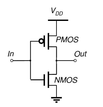
Figure 3. Schematic diagram of a CMOS inverter.
3. Analysis of propagation delay
In the preceding paragraph, we have defined the propagation delay and indicated that this article discusses the analysis of input rising ramps. To further analyze the propagation delay, it is necessary to define the rise and fall times. The rise time ( \( {t_{r}} \) ) is defined as the duration it takes for the output signal level of a circuit to transition from 0.1 \( {V_{DD}} \) to 0.9 \( {V_{DD}} \) . This definition is established to capture the signal voltage transition process from high to low, taking into account practical experience and engineering applicability. The fall time ( \( {t_{f}} \) ) is similarly defined as the duration taken for the output signal level to fall from 0.9 \( {V_{DD}} \) to 0.1 \( {V_{DD}} \) . It can be inferred from this that the propagation delay ( \( {t_{d}} \) ) consists of two components: the rise delay of the preceding stage. So, in most cases, the propagation delay of a CMOS inverter can be approximated as half the sum of the rise time and fall time [2], so the delay can be defined as:
\( {t_{d}}=\frac{{t_{r}}}{2}+\frac{{t_{f}}}{2} \ \ \ (1) \)
Fig 4 is the graphical illustration about these definitions.
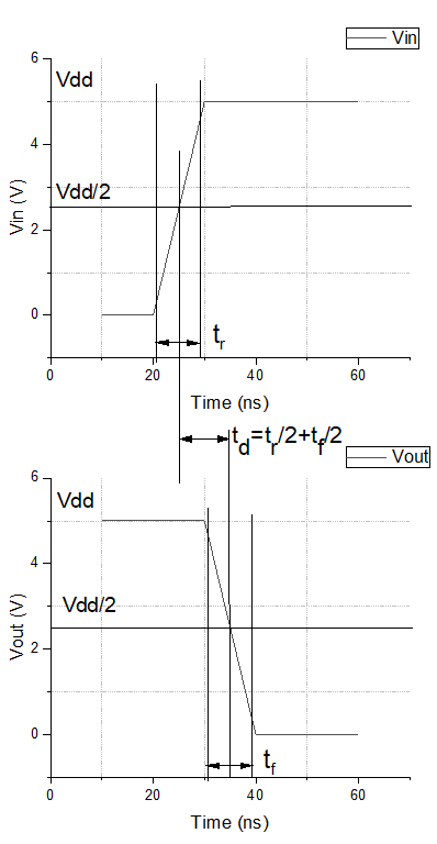
Figure 4. Rise time, fall time, and propagation delay.
According to the switching response characteristics of a CMOS inverter, we can deduce that the fall time \( {t_{f}} \) is composed of two parts. One part is the fall time \( {t_{s}} \) when the NMOS transistor operates in the saturation region, and the other part is the fall time \( {t_{l}} \) when the NMOS transistor operates in the linear region. In the saturation region of an NMOS transistor, the output voltage decreases from 0.9 \( {V_{DD}} \) to \( {V_{DD}} \) - \( {V_{TH}} \) . And in the linear region, the output voltage of the NMOS transistor decreases from \( {V_{DD}} \) - \( {V_{TH}} \) to 0.1 \( {V_{DD}} \) . And according to the output characteristics of an NMOS transistor, when the NMOS transistor operates in the saturation region (0< \( {V_{GS}} \) - \( {V_{TH}} \) ≤ \( {V_{DS}} \) ):
\( {I_{DS=0.5β{({V_{GS}}- {V_{TH}})^{2}}}} \ \ \ (2) \)
And when the NMOS transistor operates in the linear region ( \( {V_{GS}} \) - \( {V_{TH}} \) > \( {V_{DS}} \) ):
\( {I_{DS}}=β[({V_{GS}}-{V_{TH}}){V_{DS}}-{{V_{DS}}^{2}}]\ \ \ (3) \)
So according to Equations (2) and (3):
\( {t_{s}}=\int _{{V_{DD}}-{V_{TH}}}^{0.9{V_{DD}}}\frac{{C_{L}}}{{I_{DS}}}{dV_{out}}=2\frac{{C_{L}}}{{{β_{n}}({V_{DD}}-{V_{TH}})^{2}}}\int _{{V_{DD}}-{V_{TH}}}^{0.9{V_{DD}}}{dV_{out}}=\frac{2{C_{L}}({V_{TH}}-0.1{V_{DD}})}{{β_{n}}{({V_{DD}}-{V_{TH}})^{2}}} \ \ \ (4) \)
\( \begin{array}{c} {t_{l}}=\int _{0.1{V_{DD}}}^{{V_{DD}}-{V_{TH}}}\frac{{C_{L}}}{{I_{DS}}}{dV_{out}}=\frac{{c_{L}}}{{β_{n}}({V_{DD}}-{V_{TH}})}\int _{0.1{V_{DD}}}^{{V_{DD}}-{V_{TH}}}\frac{{dV_{out}}}{\frac{{{V_{out}}^{2}}}{2({V_{DD}}-{V_{TH}})}-{V_{out}}} \\ =\frac{{C_{L}}}{{β_{n}}({V_{DD}}-{V_{TH}})}ln{(\frac{19{V_{DD}}-20{V_{TH}}}{{V_{DD}}})} \ \ \ (5) \end{array} \)
Thus, we can get the fall time \( {t_{f}} \) :
\( {t_{f}}={t_{s}}+{t_{l}}=2\frac{{C_{L}}}{{β_{n}}{V_{DD}}(1-\frac{{V_{TH}}}{{V_{DD}}})}[\frac{10\frac{{V_{TH}}}{{V_{DD}}}-1}{10-10\frac{{V_{TH}}}{{V_{DD}}}}+\frac{1}{2}ln{(19-20\frac{{V_{TH}}}{{V_{DD}}})}]\ \ \ (6) \)
Based on the derivation of the fall time mentioned above, similarly, an analogous expression for the rise time \( {t_{r}} \) can be obtained:
\( {t_{r}}=2\frac{{C_{L}}}{{β_{P}}{V_{DD}}(1-\frac{{V_{TH}}}{{V_{DD}}})}[\frac{(10\frac{{V_{TH}}}{{V_{DD}}}-1)}{10-10\frac{{V_{TH}}}{{V_{DD}}}}+\frac{1}{2}ln{(19-20\frac{{V_{TH}}}{{V_{DD}}})}]\ \ \ (7) \)
From Equations (1), (6) and (7), the propagation delay \( {t_{d}} \) can be calculated:
\( {t_{d}}=\frac{{C_{L}}}{({V_{DD}}-{V_{TH}})}[\frac{10\frac{{V_{TH}}}{{V_{DD}}}-1}{10-10\frac{{V_{TH}}}{{V_{DD}}}}+\frac{1}{2}ln{(19-20\frac{{V_{TH}}}{{V_{DD}}})}](\frac{1}{{β_{n}}}+\frac{1}{{β_{p}}})\ \ \ (8) \)
It is worth noting that this computational method serves as a rough estimation technique, and there might be some discrepancies with the actual propagation delay. For more accurate calculations, reference can be made to [3].
4. Sources of propagation delay
So far, we have presented a comprehensive model and an estimation equation (8) for propagation delay, along with its mathematical analysis. Since we have essentially completed the mathematical analysis, we analyze the sources of propagation delay. According to equation (8), we can determine that the propagation delay of a CMOS inverter is primarily influenced by three factors: load capacitance, device gain, and power supply voltage. Therefore, we can conclude that the sources of propagation delay are large load capacitance, small transconductance parameter, and inadequate power supply voltage.
4.1. Load Capacitance
Load capacitance refers to the external capacitive load connected to the output node of a circuit. It represents the total capacitance that the output stage of a device needs to drive and is typically represented as \( {C_{L}} \) , it plays a significant role in determining the propagation delay in a CMOS inverter. When an input signal transitions, whether from a logic low to a logic high or vice versa, the load capacitance needs to be charged or discharged accordingly, depending on the logic level being switched. This charging or discharging process takes time and introduces a delay in the signal propagation. The time required to complete the charging or discharging of the load capacitance is affected by two primary factors: the current capability of the CMOS inverter and the magnitude of the capacitance itself. In essence, a larger load capacitance demands a greater amount of charge or discharge current, which in turn prolongs the propagation delay. This is because the CMOS inverter needs more time to transfer the necessary charge to or from the load capacitance. The relationship between the load capacitance, the CMOS inverter’s resistance, and the propagation delay can be encapsulated by the time constant τ. A larger load capacitance results in a more time constant, which, in practical terms, implies that it takes a longer duration to attain the desired voltage level. Consequently, this extended time to reach the target voltage level translates into an increased propagation delay.
4.2. Transconductance Parameter
The transconductance parameter β is an important factor in MOSFET modeling and characterization. In a MOSFET, β is defined as the ratio of the change in \( {I_{DS}} \) to the associated change of \( {({V_{GS}}-{V_{TH}})^{2}} \) . It is often denoted as the symbol β or k, and its value depends on the specific characteristics of the MOSFET, such as its geometry, oxide thickness, and mobility of the carriers. In a CMOS inverter, there are two different parts: the transconductance parameter of NMOS \( {β_{n}} \) and the transconductance parameter of PMOS \( {β_{p}} \) . They both affect various aspects of the device’s behavior, including its gain, output characteristics and operating region together. When examining the relationship between the transconductance parameter and the propagation delay of a CMOS inverter, it’s known that the transconductance parameter (β) affects the channel conductance and, thus, the speed at which the transistors can charge or discharge the load capacitance. A higher value of β indicates a higher channel conductance and, consequently, a faster charging or discharging process. This leads to a shorter propagation delay because the voltage at the output node can change more quickly in response to an input signal transition. On the other hand, a lower value of β results in a slower charging or discharging process and a longer propagation delay. The voltage at the output node takes more time to respond to the input signal change. Therefore, the relationship between β and propagation delay is such that a larger transconductance parameter generally corresponds to a shorter propagation delay, while a smaller transconductance parameter leads to a longer propagation delay.
4.3. Power Supply Voltage
The propagation delay of a CMOS inverter is significantly influenced by the power supply voltage ( \( {V_{DD}} \) ). The strength of the electric field across the gate of the MOS transistors in a CMOS inverter is directly impacted by the power supply voltage. Higher power supply voltages result in stronger electric fields, which enable faster charge/discharge of the transistor capacitances, leading to shorter propagation delays. On the other hand, lower power supply voltages reduce the electric field strength, resulting in slower charge/discharge of the transistor capacitances and longer propagation delays.
It’s important to note that a trade-off is associated with power supply voltage selection. While higher power supply voltages can reduce the propagation delay, they also increase power consumption and may lead to higher heat dissipation. Lower power supply voltages can help improve energy efficiency but at the cost of longer propagation delays. Especially in submicron and deep submicron electronic devices, using a higher power supply voltage may more likely lead to increased power consumption and other problems like device reliability issues and compatibility constraints. As the feature size shrinks [4], the available on-chip area for power supply pads and routing becomes limited. This limitation can restrict the power supplied to the device, leading to a voltage drop when the power demands exceed the supply capability. In fact, because of the factors mentioned above, the decrease in power supply voltage is one of the most crucial problems that will limit the performance of an integrated circuit [5]. Therefore, designers must carefully balance the voltage to optimize performance while mitigating voltage drop issues. In designing a CMOS inverter, the power supply voltage must be carefully chosen to strike a balance between achieving desired performance such as shorter propagation delay and managing power consumption and heat dissipation.
5. Reduction
After analyzing the propagation delay of CMOS inverters and discussing its sources, we can further explore methods for reducing propagation delay. In this article, we propose three approaches: high-k gate dielectrics, low-resistance interconnects, and layout design techniques, all of which can contribute to the reduction of propagation delay to a certain extent. Next, we will provide further explanations for each of the aforementioned methods.
5.1. High-k Gates Dielectrics
First, In the context of semiconductor materials and electronics, “k” refers to the relative permittivity or dielectric constant (also known as the “k-value”) of a material. The dielectric constant is an indicator of how well a material can store electrical energy in an electric field. It quantifies a material’s capacity to polarize in reaction to an applied electric field. A high-k dielectric material has a higher dielectric constant compared to traditional materials like silicon dioxide (SiO2). High-k materials can be used as gate dielectrics in CMOS transistors to improve performance by reducing gate capacitance. Also, when a high-k material is used, a thicker effective oxide layer can be achieved, enabling better gate control and higher drive currents in the transistor. This leads to faster switching speeds and reduced propagation delay in CMOS circuits. In the fabrication of CMOS inverters, commonly accepted high-k materials can be employed, such as Hafnium oxide (HfO2), aluminum oxide (Al2O3), and tantalum oxide (Ta2O5). According to [6], the property of SiO2, HfO2 and Ta2O5 is given in Table1 to show the comparison (especially difference in the dielectric constant) between high-k materials and the traditional materials (SiO2). Moreover, high-k materials have been extensively tested in manufacturing practices, and the utilization of these materials has shown promising improvements in reducing propagation delay. According to research findings, transistors utilizing High-K/Metal Gate Stack technology exhibit over a 25% enhancement in drive current when contrasted with the traditional SiO(N)/poly-Si baseline [7].
Table 1. The property of SiO2, HfO2 and Ta2O5 [6].
Material | \( {ε_{r}} \) | Conduction Band Offset | Stability with Si |
SiO2 | 3.9 | 3.5 | yes |
HfO2 | 22 | 1.5 | yes |
Ta2O5 | 25-30 | 0.3 | no |
5.2. Low-resistance Interconnects
In the context of a CMOS inverter, low-resistance interconnect refers to the wiring or metal interconnect layers that connect the different components of the inverter circuit, such as transistors, resistors, and capacitors. These interconnects are typically made of conductive materials, such as copper or aluminum, and are used to transmit electrical signals between the various components. In CMOS inverters, low-resistance interconnects are critical in reducing propagation delay by minimizing the voltage drop and energy loss caused by resistance. They enable faster and more efficient transmission of signals, resulting in improved overall performance of the CMOS inverter. When low-resistance interconnects are used, the voltage drop along the interconnect is minimized. This means that the output voltage of the inverter can reach its final value faster, resulting in a shorter propagation delay. Conversely, with higher interconnect resistance, more voltage is lost along the interconnect, causing a slower rise or fall time of the output voltage and thus increasing the propagation delay.
In addition, low-resistance interconnects also help to reduce RC (resistance-capacitance) delay, which is caused by the combined effect of interconnect resistance and parasitic capacitance. The reduced resistance in the interconnects lowers the RC time constant and allows for faster charging and discharging of parasitic capacitances associated with the interconnects.
Currently, multilayer graphene (MLG) and carbon nanotubes (CNT), which are promising materials with lower resistance, can be utilized as alternatives to traditional materials like copper and aluminum to achieve a reduction in propagation delay. MLG and CNT are anticipated to serve as alternative materials for downsized interconnects with nanometer-scale widths, owing to their exceptional properties [8-10]. MLG, a two-dimensional sheet of carbon atoms arranged in a hexagonal lattice, exhibits remarkable electrical conductivity, surpassing that of copper. It possesses high carrier mobility and near-ballistic transport behavior, allowing for efficient electron flow through the material. MLG also has high mechanical strength, chemical stability, and excellent thermal properties. These attributes make MLG a promising candidate for interconnects, as it can potentially offer lower resistance and enable faster signal propagation. Similarly, CNTs, which are one-dimensional carbon structures with a cylindrical shape, exhibit outstanding electrical properties. They possess extremely high current carrying capacity and low resistivity due to their unique ballistic transport behavior. CNTs also have superior mechanical strength and excellent thermal conductivity. The nanometer-scale diameter of CNTs makes them compatible with the scaled-down dimensions of interconnects in nanoscale electronic devices. These properties make CNTs an attractive option for interconnect applications, potentially leading to reduced resistance and improved performance of nanometer-scale interconnects. Both MLG and CNTs offer the potential to overcome the limitations of traditional materials such as copper and aluminum in terms of resistance, scalability, and electrical performance.
5.3. Layout Design Techniques
The layout design of a CMOS inverter is of instrumental importance in influencing the propagation delay of the circuit. The layout design comprises several crucial factors that impact the delay between input signal changes and corresponding output signal changes. For example, transistor sizing and placement are vital in determining drive strength and current capacity, ensuring balanced rise and fall times to minimize propagation delay. The lengths of interconnects and metal wires connecting the transistors affect overall delay, as longer wiring introduces additional resistance and capacitance. Effective routing techniques and minimizing wire lengths help reduce delays. Careful layout techniques, such as optimized spacing, shielding, and low-resistance materials, can mitigate parasitic effects. Efficient power supply and ground connections are fundamental to minimizing voltage fluctuation and resistance-related delay. Symmetry and matching in transistor and interconnect layout enhance overall delay performance.
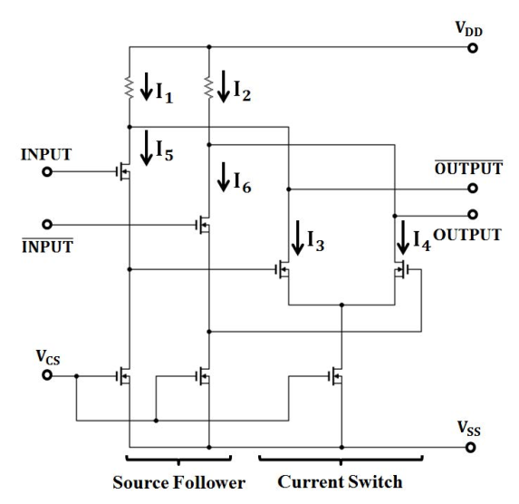
Figure 5. The Source Follower [11].
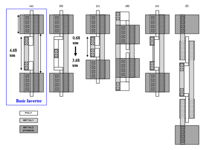
Figure 6. Basic inverter layout and case-by-case inverter layout [12].
By considering these factors and employing proper layout design techniques, such as careful transistor sizing, component placement, routing optimization, and minimizing parasitic effects, it is possible to achieve faster propagation through the CMOS inverter. For instance, employing a method known as the “source follower” technique can result in a decrease of approximately 40% in the 0.18-μm CMOS SCL circuit [11]. This layout design technique can help enhance switch current thus reduce the propagation delay. Fig5. is the demonstration of this “source follower” layout design technique. And another technique called “case-by-case” can also reduce the propagation delay 7.318% in a 0.18-μm CMOS circuit by changing the width and length of input and output nodes and the metal power position [12]. Fig6. Is the demonstration of this “case-by-case” layout design technique and the difference between the basic inverter layout. By tailoring our circuit designs based on specific requirements, and employing various appropriate layout design techniques, we can reduce propagation delay to meet our circuit’s speed requirements.
6. Conclusion
This paper provides a comprehensive and detailed discussion of the propagation delay in CMOS inverters, including mathematical analysis, sources, and reduction techniques. Through mathematical analysis, the underlying mechanisms and sources of the propagation delay are comprehensively explored, enabling the identification of potential improvement strategies based on these sources. The major sources of propagation delay in CMOS inverters encompass large load capacitance, small transconductance parameters, and inadequate power supply voltage. Meanwhile, methods to reduce propagation delay include: utilizing high-k dielectric gate materials, implementing low-resistance interconnects, and employing advanced layout design techniques. By reducing the propagation delay in CMOS inverters, we can enhance the operational speed of digital integrated circuits and improve circuit performance.
References
[1]. L. Bisdounis, S. Nikolaidis, and O. Koufopavlou. (1998) Analytical Transient Response and Propagation Delay Evaluation of the CMOS Inverter for Short-Channel Devices. IEEE J. Solid-State Circuits, 33:302-306.
[2]. Zhongjie Xue. (2002) Empirical Models and Estimation of Delay Time in CMOS Gate Circuits. China Integrated Circuit, 33:52-57.
[3]. T. Sakurai and A. R. Newton. (1990) Alpha-power law MOSFET model and its applications to CMOS inverter delay and other formulas. IEEE J. Solid-State Circuits, 25: 584–594.
[4]. Liqiong Wei and Kaushik Roy. (2000) Low Voltage Low Power CMOS Design Techniques for Deep Submicron ICs. In: Wireless and Digital Imaging in the Millennium, Proceedings of 13th International Conference on VLSI Design. Calcutta. pp.12.
[5]. Tomohiro Fujitu and Hidetoshi Onoderu. (2000) Statistical Delay Calculation with Vector Synthesis Model. In: 2000 IEEE International Symposium on Circuits and Systems. Geneva. pp.473-476.
[6]. Mitashra Gupta and Ashutosh Nandi. (2017) Impact of Matched High-K Gate Dielectric based DG-MOSFET on SRAM performance. In: 2017 4th International Conference on Power, Control & Embedded Systems (ICPCES). Allahabad. pp.1-5.
[7]. M. Chudzik, et al. (2007) High-Performance High-K/Metal Gates for 45nm CMOS and Beyond with Gate First Processing. In: Proceedings of 20th International Conference on VLSI Design. Bangalore. pp.97-198.
[8]. J. Kong, E. Yenilmez, T. W. Tombler, W. Kim, and H. Dai. (2001) Quantum Interference and Ballistic Transmission in Nanotube Electron Waveguides. Phys. Rev. Lett., 87:6801.
[9]. J. Hone, M. Whitney, C. Piskoti, and A. Zettl. (1999) Thermal conductivity of single-walled carbon nanotubes. Phys. Rev. B, 59: 2514.
[10]. Zhen Yao, Charles L. Kane, and Cees Dekker. (2000) High-Field Electrical Transport in Single-Wall Carbon Nanotubes. Phys. Rev. Lett., 84: 2941.
[11]. Yuki Hagita and Kiyoshi Ishii. (2012) Circuit Technique for Improving Propagation Delay Times in CMOS Source-Coupled Logic Circuits. In: 2012 IEEE International Symposium on Intelligent Signal Processing and Communication Systems. Tamsui. pp.615-618.
[12]. Ji-Hak Yu, Chan-Keun Kwon, Junil Moon and Soo-Won Kim. (2015) An Inverter Layout Technique for Propagation Delay Minimization. In: 2015 IEEE International Symposium on Consumer Electronics. Madrid. pp.1-2.
Cite this article
Lan,Z. (2024). On the propagation delay of CMOS inverters. Applied and Computational Engineering,84,163-172.
Data availability
The datasets used and/or analyzed during the current study will be available from the authors upon reasonable request.
Disclaimer/Publisher's Note
The statements, opinions and data contained in all publications are solely those of the individual author(s) and contributor(s) and not of EWA Publishing and/or the editor(s). EWA Publishing and/or the editor(s) disclaim responsibility for any injury to people or property resulting from any ideas, methods, instructions or products referred to in the content.
About volume
Volume title: Proceedings of the 4th International Conference on Materials Chemistry and Environmental Engineering
© 2024 by the author(s). Licensee EWA Publishing, Oxford, UK. This article is an open access article distributed under the terms and
conditions of the Creative Commons Attribution (CC BY) license. Authors who
publish this series agree to the following terms:
1. Authors retain copyright and grant the series right of first publication with the work simultaneously licensed under a Creative Commons
Attribution License that allows others to share the work with an acknowledgment of the work's authorship and initial publication in this
series.
2. Authors are able to enter into separate, additional contractual arrangements for the non-exclusive distribution of the series's published
version of the work (e.g., post it to an institutional repository or publish it in a book), with an acknowledgment of its initial
publication in this series.
3. Authors are permitted and encouraged to post their work online (e.g., in institutional repositories or on their website) prior to and
during the submission process, as it can lead to productive exchanges, as well as earlier and greater citation of published work (See
Open access policy for details).
References
[1]. L. Bisdounis, S. Nikolaidis, and O. Koufopavlou. (1998) Analytical Transient Response and Propagation Delay Evaluation of the CMOS Inverter for Short-Channel Devices. IEEE J. Solid-State Circuits, 33:302-306.
[2]. Zhongjie Xue. (2002) Empirical Models and Estimation of Delay Time in CMOS Gate Circuits. China Integrated Circuit, 33:52-57.
[3]. T. Sakurai and A. R. Newton. (1990) Alpha-power law MOSFET model and its applications to CMOS inverter delay and other formulas. IEEE J. Solid-State Circuits, 25: 584–594.
[4]. Liqiong Wei and Kaushik Roy. (2000) Low Voltage Low Power CMOS Design Techniques for Deep Submicron ICs. In: Wireless and Digital Imaging in the Millennium, Proceedings of 13th International Conference on VLSI Design. Calcutta. pp.12.
[5]. Tomohiro Fujitu and Hidetoshi Onoderu. (2000) Statistical Delay Calculation with Vector Synthesis Model. In: 2000 IEEE International Symposium on Circuits and Systems. Geneva. pp.473-476.
[6]. Mitashra Gupta and Ashutosh Nandi. (2017) Impact of Matched High-K Gate Dielectric based DG-MOSFET on SRAM performance. In: 2017 4th International Conference on Power, Control & Embedded Systems (ICPCES). Allahabad. pp.1-5.
[7]. M. Chudzik, et al. (2007) High-Performance High-K/Metal Gates for 45nm CMOS and Beyond with Gate First Processing. In: Proceedings of 20th International Conference on VLSI Design. Bangalore. pp.97-198.
[8]. J. Kong, E. Yenilmez, T. W. Tombler, W. Kim, and H. Dai. (2001) Quantum Interference and Ballistic Transmission in Nanotube Electron Waveguides. Phys. Rev. Lett., 87:6801.
[9]. J. Hone, M. Whitney, C. Piskoti, and A. Zettl. (1999) Thermal conductivity of single-walled carbon nanotubes. Phys. Rev. B, 59: 2514.
[10]. Zhen Yao, Charles L. Kane, and Cees Dekker. (2000) High-Field Electrical Transport in Single-Wall Carbon Nanotubes. Phys. Rev. Lett., 84: 2941.
[11]. Yuki Hagita and Kiyoshi Ishii. (2012) Circuit Technique for Improving Propagation Delay Times in CMOS Source-Coupled Logic Circuits. In: 2012 IEEE International Symposium on Intelligent Signal Processing and Communication Systems. Tamsui. pp.615-618.
[12]. Ji-Hak Yu, Chan-Keun Kwon, Junil Moon and Soo-Won Kim. (2015) An Inverter Layout Technique for Propagation Delay Minimization. In: 2015 IEEE International Symposium on Consumer Electronics. Madrid. pp.1-2.