


1. Introduction
In recent years, with the rapid development of modern science and technology, there is a growing demand for efficient and accurate imaging technology in society [1]. From medical imaging to virtual reality, from autonomous driving to the protection of cultural heritage [2], 3D imaging technology has played its unique importance and wide application potential in many fields, 3D imaging technology has played its unique importance and wide application potential in many fields. Although traditional 2D images can provide certain information, they are far less accurate and informative compared with 3D imaging. By capturing the three-dimensional structural information of an object, 3D imaging technology can provide more comprehensive and accurate image data, thus significantly improving performance and effect in various applications.
Under this background, image sensor technology is also progressing and evolving. CMOS sensors, as an emerging type of image sensors, are rapidly taking over the market and gradually replacing traditional sensors. This is due to their high resolution, low power consumption, small size, and high integration. They have gained significant attention in various applications over the past decade [3]. CMOS sensors are not only widely used in consumer electronics such as digital cameras and phones, but also play an important role in areas like industrial testing, autonomous driving, and scientific research. However, how to fully utilize the advantages of CMOS sensors to develop high-precision and real-time 3D imaging technology is still a technical challenge to be solved around the world. Current 3D imaging technologies mainly include time-of-flight, structured light, stereo vision, and other methods [4]. However, each of these methods has its own advantages and disadvantages in terms of accuracy, real-time performance, and cost. A lot of research and exploration are still required to find the optimal balance in practical applications.
Based on this background, this paper will focus on real-time 3D imaging technology based on CMOS sensors. It will first introduce how CMOS sensors work. CMOS sensors convert light into electrical signals using photodiodes and amplify and digitize these signals with internal circuitry. Then there is an introduction to the real-time 3D imaging technology. Real-time 3D imaging technology captures the three-dimensional structure of objects using optical, electronic, and computational techniques. Finally, the real-time 3D imaging technology based on CMOS sensors is introduced. This technology utilizes the high resolution and fast response characteristics of CMOS sensors, combined with advanced image processing algorithms, to achieve accurate and efficient 3D imaging. This research aims to introduce innovative concepts and technical supports to advance related fields, thereby fostering the broader adoption and implementation of 3D imaging technology in various practical applications.
2. CMOS sensors
RadhaKrishna et al. provide a thorough review of the working principles and comparative advantages of CMOS and CCD (Charge-Coupled Device) image sensors, which are essential components in modern digital imaging devices such as cameras and mobile phones [5]. The paper presents a comprehensive overview of how image sensors convert photons into electrical signals, a fundamental process for digital imaging and explains the different mechanisms employed by CMOS and CCD sensors for this conversion. CMOS sensors convert photon intensity directly to voltage, while CCD sensors convert photons to electrons first and then to voltage. It includes block diagrams and technical descriptions to help illustrate the functional differences between the two sensor types.
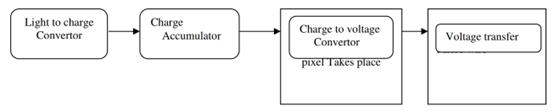
Figure 1. CMOS sensor block diagram [5].
Based on a detailed comparison of CMOS and CCD sensors, CMOS sensors are praised for their high-speed signal readout and low power consumption, making them suitable for small, cost-effective devices such as mobile phones and cameras. The paper explains that the pixel in a CMOS sensor comprises a photodiode and a CMOS transistor acting as a switch. The paper suggests that ongoing technological advancements could lead to CMOS sensors achieving image quality comparable to that of CCD sensors. This potential development could significantly impact the choice and application of image sensors in the future. Overall, this paper emphasizes the importance of understanding the specific requirements of different imaging applications and choosing the appropriate sensor technology accordingly. Moreover, it highlights the potential for future advancements in CMOS technology to further enhance its application scope and image quality. As shown in figure 1.
Having discussed CMOS sensors, it is worth noting that HDR (High Dynamic Range) CMOS sensors, as their advanced version, overcome the limitations of traditional CMOS sensors in high dynamic range scenes. Takayanagi et al. provide an in-depth analysis of the advancements and applications of HDR CMOS sensor technology within the automotive sector [6]. He also highlights the critical need for HDR image capture in automotive applications due to the HDR of brightness in various operational scenarios. This requirement is paramount for enhancing the safety and automation of driving systems. The paper discusses multiple exposure HDR methods and the associated challenges, such as LED flicker caused by time aliasing effects and motion artifacts, providing a comprehensive overview of the technical difficulties and potential solutions. The paper reviews several advanced HDR technologies developed for automotive applications, emphasizing recent fabrication advancements like backside illumination processes and pixel-level hybrid wafer bonding. These innovations have created new trends in HDR technology, enhancing performance and addressing previous limitations. The introduction of single-exposure/single-PD schemes is highlighted as fundamentally suitable for maintaining image information across various optical conditions without significant loss. The paper emphasizes the potential for further improvement in HDR technology performance and functionality, suggesting that ongoing advancements could significantly enhance its applications in the future. The use of pixel-level stacking technology is expected to enhance HDR schemes, adding functions such as in-pixel data compression, signal processing, and real-time sensing and control with high efficiency. The paper presents a detailed examination of application requirements, fundamental HDR approaches, technological trends, and the advantages and disadvantages of HDR CMOS sensor for automotive uses, highlighting key innovations and their implications for enhancing safety and automation in the automotive industry, along with future prospects for HDR technology.
3. Real-time 3D Imaging Technology
3D imaging technology has been widely used in many fields, especially in the medical imaging area. For instance, Singh et al. review the significant advancements and applications of 3D CNNs (convolutional neural networks) in medical imaging [7]. The rapid progress in machine learning, coupled with improvements in graphics processing technologies and the availability of medical imaging data, has greatly increased the adoption of deep learning models in the medical field. Then he traces the evolution of 3D CNNs from their roots in machine learning, detailing their development and mathematical underpinnings. This includes the foundational principles of 3D CNNs and the preprocessing steps required for medical images before they are processed by these networks.
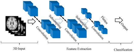
Figure 2. Typical architecture of 3D CNN [7].
A significant portion of the paper reviews how 3D CNNs are employed across various medical imaging tasks such as classification, segmentation, detection, and localization, highlighting the diverse applications and the benefits they bring to medical diagnostics. These applications demonstrate the capability of 3D CNNs to analyze complex volumetric medical data, improving the efficiency and accuracy of diagnoses. He compares 3D CNNs with traditional 2D CNNs and highlights the unique challenges associated with 3D medical image analysis. These include the high computational cost, limited availability of training data, and the curse of dimensionality. The paper discusses how these challenges are addressed through advancements in neural network architectures, data augmentation techniques, and the use of high-performance GPUs. The main results show that the use of 3D CNNs in medical imaging has led to significant improvements in the automated analysis of complex 3D medical data, providing more precise and reliable diagnostic tools. Despite the computational challenges, the paper demonstrates that 3D CNNs can achieve remarkable performance, potentially matching or even surpassing human-level accuracy in certain tasks. As shown in figure 2.
Tobin et al. explore the application of ToF (time-of-flight) LiDAR using single-photon detection for three-dimensional imaging in challenging scenarios [8]. These include imaging over long distances and through highly scattering environments like fog and smoke. He details the use of TCSPC (time-correlated single-photon counting) in LiDAR systems, leveraging its high sensitivity to enable low power, high-resolution imaging even in difficult measurement conditions. He also highlights the use of SNSPDs (superconducting nanowire detectors) and SPAD (single-photon avalanche diode) detectors, noting their capability for picosecond timing and operation near room temperature, which are critical for achieving fine surface-to-surface resolution. A key innovation presented is a robust statistically-based processing algorithm designed for real-time reconstruction of single-photon data in the presence of atmospheric obscurants. This algorithm not only reconstructs depth profiles but also provides uncertainty estimates, improving the reliability of the depth data. The paper demonstrates the capability of this technology to reconstruct depth profiles of moving objects at stand-off distances up to 150 meters to five attenuation lengths. This is a significant achievement, showcasing the potential for high-resolution 3D imaging in real-world, degraded visual environments. The processing algorithm, M2R3D, is highlighted for its efficiency, with a processing time of around 90 milliseconds per frame, enabling real-time processing with latency lower than one frame. Overall, this paper provides a compelling case for the use of single-photon detection in LiDAR systems for 3D imaging, demonstrating substantial advancements in imaging resolution, real-time processing, and applicability in challenging scenarios.
4. Real-time 3D Imaging Technology Based on CMOS Sensors
Following the discussion on CMOS sensors and 3D imaging, the focus shifts to integrating these technologies, specifically advancements and applications of real-time 3D imaging based on CMOS sensors.
Rogers et al. present significant advancements in real-time 3D imaging technology using a large-scale coherent detector array integrated with CMOS technology [9]. Notably, the paper demonstrates the first large-scale coherent detector array consisting of 512 pixels, a significant improvement over previous systems restricted to fewer than 20 pixels. This advancement is achieved through the monolithic integration of photonic and CMOS electronic circuits, allowing for straightforward scaling to larger arrays.
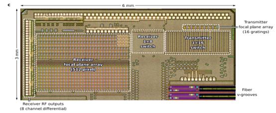
Figure 3. Optical micrograph of the demonstrator chip [9].
The integration of solid-state beam steering with the coherent receiver array eliminates trade-offs between field of view and range, while the FMCW (frequency-modulated continuous-wave) LiDAR scheme provides several advantages over traditional time-of-flight LiDAR, including immunity to sunlight interference and direct measurement of target velocity. The integration of solid-state beam steering with the coherent receiver array eliminates trade-offs between field of view and range. The system employs a FMCW LiDAR scheme, which provides several advantages over traditional time-of-flight LiDAR, including immunity to sunlight interference and direct measurement of target velocity. The actively multiplexed readout architecture allows for efficient mapping of 512 pixels to 8 outputs, enabling real-time data acquisition and processing. In conclusion, this paper introduces a groundbreaking 3D imaging architecture that combines high performance, scalability, and low cost using CMOS technology. This positions it as a potential universal solution for diverse 3D imaging applications. As shown in figure 3.
Radamson et al. provide a comprehensive review of the advancements in nano-scale transistor technology as the semiconductor industry approaches the end of ITRS (the International Technology Roadmap for Semiconductors) [10]. The focus is on new architectures, simulation methods, and process technologies that are driving the evolution of CMOS transistors into unknown territories.
The paper first begins with a discussion of the transition from traditional planar 2D transistors to advanced 3D structures, such as Fin Field-Effect Transistors (FinFETs) and Gate-All-Around FETs (GAAFETs). These new designs improve control over short-channel effects and enhance carrier mobility, making them suitable for continued scaling beyond the 10 nm technology node. The importance of device simulation using advanced Technology Computer-Aided Design (TCAD) models is emphasized. These models range from quantum-mechanical to semi-classical approaches, providing accurate predictions of device behavior at nano-scale dimensions. Then the paper discusses various metrology techniques for in-line monitoring and nano-analysis, including advanced electron microscopy, 3D atom force microscopy, and X-ray techniques. These methods are essential for ensuring the quality and reliability of nano-scale transistors during fabrication. The integration of high-mobility materials and the use of advanced metrology techniques ensure that future nano-scale transistors meet the demanding requirements of modern electronics. Overall, this paper provides a detailed overview of the current state and future directions of CMOS technology, emphasizing the innovative approaches needed to continue scaling transistors in the post-ITRS era. The comprehensive review of materials, processes, and metrology techniques highlights the challenges and potential solutions for developing the next generation of high-performance nano-scale transistors.
Building on the advancements in hybrid CMOS-photonics chip design for 3D imaging, Jahromi et al. further explore the development of a single-chip receiver for pulsed laser dTOF (direct time-of-flight) 3D imaging, leveraging CMOS technology to achieve high sensitivity and resolution [11]. This paper presents a highly innovative single-chip receiver designed for pulsed laser dTOF 3D imaging applications, implemented using 0.35-µm high-voltage (HV) CMOS technology. The chip features a 32 × 128 single-photon avalanche diode (SPAD) array with a 35% fill factor and 257 time-to-digital converters (TDCs) with approximately 78-ps resolution, showcasing significant advancements in solid-state 3D imaging technology. The paper details the integration of a SPAD array and TDCs on a single chip. The SPAD array is divided into blocks, with each block sharing TDC resources dynamically. Consequently, this design achieves a high fill factor and allows efficient resource allocation, significantly enhancing the system's spatial resolution and efficiency. The SPADs operate in gated mode, which helps suppress detections caused by dark and background light, enhancing the system's sensitivity. Time gating with a 5-ns resolution further reduces background noise, improving measurement accuracy. The chip is tested in a solid-state 3D range imager setup with flood-pulsed illumination from a laser diode (LD)-based transmitter, producing short, high-energy pulses. Overall, this paper introduces a highly efficient and scalable receiver IC for dTOF 3D imaging applications, leveraging the integration of SPAD and TDC arrays on a single chip using CMOS technology. The innovative design and efficient use of optical power make it a promising solution for various 3D imaging applications, including autonomous navigation, gesture recognition, and face recognition.
Building on the advancements in nano-scale CMOS technology, Morimoto et al. demonstrate a high-resolution 1 Megapixel SPAD camera fabricated in 180 nm CMOS image sensor technology [12]. This showcases the application of CMOS innovations in high-speed, high-resolution 3D imaging. The sensor captures 2D and 3D scenes over a distance of 2 meters, with a resolution (least significant bit) of 5.4 mm and a precision better than 7.8 mm (root mean square). The paper demonstrates extended dynamic range in dual exposure operation mode and spatially overlapped multi-object detection in single-photon time-gated ToF experiments. Based on the experiment, the sensor achieves a high depth precision with a fine gate scanning pitch, demonstrating the capability to measure distances with high accuracy and precision. The main results show that the camera's time-gated SPAD sensor achieves high dynamic range 2D imaging and high spatiotemporal resolution 3D imaging, demonstrating its superior performance. Besides, the system shows the ability to detect spatially overlapped multi-objects with a single-photon time-gating scheme, experimentally demonstrated for the first time. Last, the SPAD array's size is the largest among state-of-the-art sensors, almost four times higher than previous works, with one of the smallest pixel pitches. Overall, this paper introduces a highly efficient and scalable SPAD camera for high-speed, high-resolution 3D imaging applications. The innovative design and performance make it suitable for a wide range of applications, including security, automotive, robotics, biomedical, and scientific research.
5. Conclusion
This paper has presented a comprehensive review and exploration of real-time 3D imaging technology based on CMOS sensors. It began by examining the fundamental principles and comparative advantages of CMOS sensors over other types of image sensors, particularly CCD sensors. The review demonstrated how CMOS sensors, with their high-speed signal readout and low power consumption, are becoming increasingly dominant in various imaging applications. It also discussed the potential for future advancements in CMOS technology, particularly in HDR imaging, which promises further enhancements in image quality and application scope.
Next, it explored the realm of real-time 3D imaging technology, focusing on its applications in medical imaging and LiDAR systems. Furthermore, the use of 3D CNNs in medical imaging was highlighted, showcasing their ability to analyze complex volumetric data and improve diagnostic accuracy. Additionally, it reviewed the application of single-photon detection in LiDAR systems, which enables high-resolution 3D imaging in challenging environments, demonstrating significant improvements in imaging resolution and real-time processing capabilities.
Finally, it delved into the integration of CMOS technology with 3D imaging systems, presenting recent advancements in large-scale coherent detector arrays and single-chip receivers for pulsed laser dTOF 3D imaging. These innovations leverage CMOS technology to achieve high sensitivity, resolution, and scalability in 3D imaging applications. The development of a 1 Megapixel SPAD camera fabricated in 180 nm CMOS technology exemplifies the practical applications of these advancements, achieving high-speed, high-resolution 3D imaging suitable for a wide range of applications including security, automotive, robotics, biomedical, and scientific research.
Overall, this paper highlights significant advancements in real-time 3D imaging technology using CMOS sensors. It demonstrates their critical role due to high resolution, low power consumption, and compact size. The innovations in SPAD cameras and large-scale detector arrays showcase the transformative potential for high-performance, scalable 3D imaging applications. Future developments will focus on higher resolution and sensitivity, and integration with AI for enhanced real-time processing and analysis.
References
[1]. Wang Q and Kim M.-K (2019). Applications of 3D point cloud data in the construction industry: A fifteen-year review from 2004 to 2018. Advanced Engineering Informatics 39, 306
[2]. Taleb A, Loetzsch W, Danz N, Severin J, Gaertner T, Bergner B, and Lippert C (2020). 3D Self-Supervised Methods for Medical Imaging. NeurIPS, 33
[3]. Sukhavasi S.B., Sukhavasi S.B., Elleithy K, Abuzneid S and Elleithy A (2021). CMOS Image Sensors in Surveillance System Applications. Sensors 21(2), 488
[4]. Gu F, Cao H, Xie P and Song Z (2022). Accurate Depth Recovery Method Based on the Fusion of Time-of-Flight and Dot-Coded Structured Light. Photonics 9(5), 333
[5]. RadhaKrishna M.V.V. et al. (2021). A review on image processing sensor. J. Phys.: Conf. Ser. 1714 012055
[6]. Takayanagi I and Kuroda R (2022). HDR CMOS Image Sensors for Automotive Applications. IEEE Trans. Electron Devices, 69, 6
[7]. Singh S.P., Wan L, Gupta S, Gol H, Padmanabhan P and Gulyás B (2020). 3D Deep Learning on Medical Images: A Review. Sensors, 20(18), 5097
[8]. Tobin R, Halimi A, McCarthy A et al. (2021). Robust real-time 3D imaging of moving scenes through atmospheric obscurant using single-photon LiDAR. Sci Rep 11, 11236
[9]. Rogers C, Piggott A.Y., Thomson D.J. et al. (2021).A universal 3D imaging sensor on a silicon photonics platform. Nature 590, 256–261
[10]. Radamson H.H., Zhu H, Wu Z et al. (2020). State of the art and future perspectives in advanced CMOS technology. Nanomaterials, 10(8), 1555
[11]. Jahromi S, Jansson J-P, Keränen P, and Kostamovaara J (2020). A 32 × 128 SPAD-257 TDC Receiver IC for Pulsed TOF Solid-State 3-D Imaging. IEEE J. Solid-State Circuits, 55, 7
[12]. Morimoto K, Ardelean A, Wu M, et al. (2020). Megapixel time-gated SPAD image sensor for 2D and 3D imaging applications. Optica 346 (7), 4
Cite this article
Zhu,Q. (2024). Research on real-time 3D imaging technology based on CMOS sensors. Applied and Computational Engineering,101,111-117.
Data availability
The datasets used and/or analyzed during the current study will be available from the authors upon reasonable request.
Disclaimer/Publisher's Note
The statements, opinions and data contained in all publications are solely those of the individual author(s) and contributor(s) and not of EWA Publishing and/or the editor(s). EWA Publishing and/or the editor(s) disclaim responsibility for any injury to people or property resulting from any ideas, methods, instructions or products referred to in the content.
About volume
Volume title: Proceedings of the 2nd International Conference on Machine Learning and Automation
© 2024 by the author(s). Licensee EWA Publishing, Oxford, UK. This article is an open access article distributed under the terms and
conditions of the Creative Commons Attribution (CC BY) license. Authors who
publish this series agree to the following terms:
1. Authors retain copyright and grant the series right of first publication with the work simultaneously licensed under a Creative Commons
Attribution License that allows others to share the work with an acknowledgment of the work's authorship and initial publication in this
series.
2. Authors are able to enter into separate, additional contractual arrangements for the non-exclusive distribution of the series's published
version of the work (e.g., post it to an institutional repository or publish it in a book), with an acknowledgment of its initial
publication in this series.
3. Authors are permitted and encouraged to post their work online (e.g., in institutional repositories or on their website) prior to and
during the submission process, as it can lead to productive exchanges, as well as earlier and greater citation of published work (See
Open access policy for details).
References
[1]. Wang Q and Kim M.-K (2019). Applications of 3D point cloud data in the construction industry: A fifteen-year review from 2004 to 2018. Advanced Engineering Informatics 39, 306
[2]. Taleb A, Loetzsch W, Danz N, Severin J, Gaertner T, Bergner B, and Lippert C (2020). 3D Self-Supervised Methods for Medical Imaging. NeurIPS, 33
[3]. Sukhavasi S.B., Sukhavasi S.B., Elleithy K, Abuzneid S and Elleithy A (2021). CMOS Image Sensors in Surveillance System Applications. Sensors 21(2), 488
[4]. Gu F, Cao H, Xie P and Song Z (2022). Accurate Depth Recovery Method Based on the Fusion of Time-of-Flight and Dot-Coded Structured Light. Photonics 9(5), 333
[5]. RadhaKrishna M.V.V. et al. (2021). A review on image processing sensor. J. Phys.: Conf. Ser. 1714 012055
[6]. Takayanagi I and Kuroda R (2022). HDR CMOS Image Sensors for Automotive Applications. IEEE Trans. Electron Devices, 69, 6
[7]. Singh S.P., Wan L, Gupta S, Gol H, Padmanabhan P and Gulyás B (2020). 3D Deep Learning on Medical Images: A Review. Sensors, 20(18), 5097
[8]. Tobin R, Halimi A, McCarthy A et al. (2021). Robust real-time 3D imaging of moving scenes through atmospheric obscurant using single-photon LiDAR. Sci Rep 11, 11236
[9]. Rogers C, Piggott A.Y., Thomson D.J. et al. (2021).A universal 3D imaging sensor on a silicon photonics platform. Nature 590, 256–261
[10]. Radamson H.H., Zhu H, Wu Z et al. (2020). State of the art and future perspectives in advanced CMOS technology. Nanomaterials, 10(8), 1555
[11]. Jahromi S, Jansson J-P, Keränen P, and Kostamovaara J (2020). A 32 × 128 SPAD-257 TDC Receiver IC for Pulsed TOF Solid-State 3-D Imaging. IEEE J. Solid-State Circuits, 55, 7
[12]. Morimoto K, Ardelean A, Wu M, et al. (2020). Megapixel time-gated SPAD image sensor for 2D and 3D imaging applications. Optica 346 (7), 4