


1. Introduction
Since the invention of MOSFET, circuit design has entered a completely new stage, formally stepping into the integrated circuit (IC) stage. Decades of development have also attracted more and more fields to interact with integrated circuits, the material properties of integrated circuits are getting better, and better, Industrial lithography is also advancing, and new circuit designs are continuously being developed, one after another. At the same time, the demand for device performance is also increasing, tiny errors can comparatively impact on the entire chip. People have to start looking at the mismatch. Fundamentally, there is a commitment to improving the precision of the manufacturing process which is the basic problem caused by mismatch. Device consistency can be improved through improved lithography, etching, and deposition techniques; people have also designed many circuit structures that can reduce mismatches, effectively utilizing the advantages of structure; after the mismatch has occurred, device mismatches can be reduced by subsequent compensatory blending. To sort out the overall ideas, this article combed through ideas for solving the mismatch problem by way of discussing main device resistance and capacitor mismatch and solutions, Current-mirror structure of structured-level circuits, operational amplifier mismatch, and chopping technology and automatic zeroing technology stacked on the circuit. hope to help establish a solution system for the mismatch.
2. Device Mismatch
2.1. Resistance mismatch
As the most basic circuit device, resistors are widely used in various circuits. Due to randomness and systematic errors in the manufacturing process, the circuit accuracy has changed. Such as the R-2R DAC circuit, the mismatch of the resistor affects the static characteristics of this circuit. To ensure the accuracy of the circuit, requirement to keep the ratio of resistive elements consistent throughout the circuits [1]. For resistors, the random errors generated during the production process can be calculated using the normal distribution, and the solution is expanding device size. The systematic errors in resistance are usually caused by external factors, which are related to the location of the device on the chip, usually improved by changing the chip layout. So there is an existing set of experimental data that suggests, the three ways to represent systematic errors are Linear Gradient, Quadratic Gradient, and Central Quadratic Gradient. Simulation of DAC circuit performance metrics over three gradients with two different types of conventional and public center layouts determines the layout of the public center has a better effect, less susceptible to systematic errors [1]. When the resistor is connected to the circuit to start operation, it will generate heat, causing the resistance temperature to rise. The change in resistance does not change linearly with increasing temperature, so a mismatch is created. To solve this type of problem, the current mainstream solution is to use temperature-sensitive resistors for temperature detection and make a series of compensations [2]. In summary, the mismatch of resistors is the fundamental mismatch, based on the best manufacturing process, need to consider more rational chip layout locations and use some compensation techniques to minimize mismatch.
2.2. Capacitor mismatch
Capacitors are also widely used devices in circuit design, because their special characteristics of “through DC, stop AC” make it have outstanding advantages in the fields of integrated circuits, communication, and energy storage. however, the mismatch still exists today. The mismatch of capacitors may cause nonlinear issues, and difficult to improve accuracy [3]. There are three mainly causes, manufacturing process deviations, parasitic and temperature effects. To solve these problems, researchers designed a solution of time-to-digital (TDC) to measure mismatches. obtain the voltage of the mismatch information first, then calculate the difference between theory and real, finally work out the real weight of capacitors, and adjust the capacitor array to solve the mismatches. The outstanding advantage of this method is that the calibration records can be stored for subsequent use.
2.3. Mismatch of metal oxide semiconductor field effect transistor
The mismatch of the Metal Oxide Semiconductor Field Effect Transistor (MOSFET) is more complex than resistors and capacitors. The manufacturing of MOSFETs is also more complex, with higher requirements for device size. Especially the coefficients such as channel width W and length L that are closely related to MOSFET performance. There is a report on MOS mismatch characterization and modeling of precision analog circuits states that MOSFET mismatch is mainly reflected in two aspects, mismatch of threshold voltage and conductivity constant [4]. Fixed oxide layer charge between devices, differences in interface trap charge and non-uniform distribution of doped atoms both will cause a mismatch in threshold voltage. In order to get some requirements, people will add additional doping to the surface layer of transistors to adjust the threshold voltage when manufacturing MOSFET. This process is called threshold adjustment implantation. Due to the uneven distribution of materials during the implantation process, the threshold voltage will also change as a result. The mismatch of conductivity constants is actually more fundamental, the influencing factors are device length L, width W, and channel mobility μ. In this report, researchers provided a comprehensive introduction on how to reduce mismatches, as shown in table 1.
Table 1. Formatting sections, subsections and subsubsections.
Research perspective | solution |
Layout | Common center layout/Cross layout |
Technology | Uniform doping/control of oxide layer growth |
Circuit design | Negative feedback technology/Circuit calibration |
Compensate | Temperature compensation |
The theory that threshold voltage mismatch is linearly related to the reciprocal of the square root of the effective channel area has been widely accepted in the fields of semiconductor device physics and microelectronics [5]. There is a new study conducted experiments on 12000 PMOS and NMOS transistors, found a channel length different from this classical theory -1.2 micrometers. Researchers have developed a new testing product and algorithm to more efficiently extract transistor adaptation parameters. After experimental testing on 12000 MOS transistors, give this new theory some data support. Finally, the experimental results proved the superiority of this algorithm in solving mismatch problems and also proved the mismatch problem of MOSFETs in a 1.2-micron channel no longer satisfies a linear relationship with the reciprocal of the square root of the effective channel area.
3. Reduce Mismatched Circuit Structures
3.1. Current mirror
Current mirror structure, also known as mirror constant current source. It means to copy the current from one circuit to another circuit, that can decrease the effect of changes in voltage, temperature, etc. affect the circuit. Connecting current sources to circuits with different loads, the load on the external circuit may affect the constant output current of the current source. After adopting the current mirror structure, the change in voltage will not affect the constant current output of the current mirror structure, so that the current source is more stable. In the design of current mirrors, people set the parameters of two MOS devices to make them more compatible. The entire structure can provide a more accurate output current close to the reference current, reducing the impact of device mismatch on the circuit. In terms of integration, the current mirror structure can be easily integrated into a single chip. It makes the design of circuit easier, and the use of external components has been reduced. When facing different needs, nested current mirror structures with multiple output currents (Figure 1) or higher-level structures such as Wilson current mirrors (Figure 2) can be designed to meet the requirements. Do not need to build external circuits, saving space. Although this structure has initially reduced the mismatch problem of the circuit, there are still mismatches. There is a report on using floating gate transistors for mismatch compensation to reduce CMOS current mirror mismatch. The sources of the current mirror mismatch were explained in the report. It includes two important mismatches, one is the change in subthreshold slope can affect the current characteristics of transistors in the weak inversion region, causing mismatch, and another one is transitioning to parameter changes [6]. The floating gate transistor compensation method proposed by Shi Ning et al. has a good compensation effect in the weak inversion region. In the weak inversion region, floating gate transistors can store charges at the gate level, generate voltage offset to compensate for threshold voltage mismatch, and reduce current mirror mismatch. However, in the strong reversal zone, although compensating for the mismatch of threshold voltage, changes in transconductance parameters still introduce gain errors. Therefore, researchers have proposed using modeling and simulation methods to theoretically adjust parameters, then use a large number of simulation results to obtain the final result. So far, there is still no direct way to reduce gain mismatch.
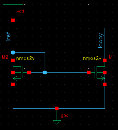
Figure 1. Ordinary current-mirror structure.
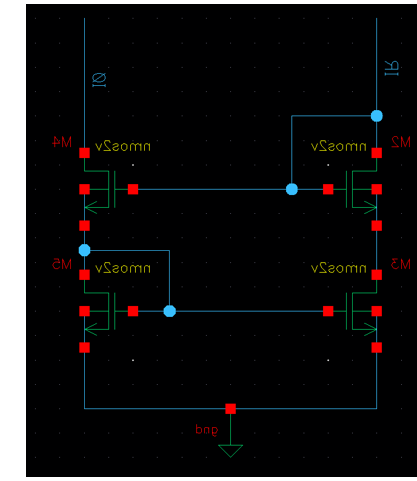
Figure 2. Wilson current mirror.
3.2. Operational amplifier
In basic operational amplifiers, they will all contain current mirrors and differential pair structures. However, the structure is not fixed, and the circuit is designed according to the requirements. It can be roughly divided into five components: input stage, gain stage, output stage, bias circuit, and compensation network. The current mirror structure mentioned earlier can be widely used in the gain stage, output stage, bias current and other parts. One of the most widely used applications at the input level is differential pairing. Operational amplifiers require high input impedance at the input end so that it will be better isolated from the previous level signal to ensure that the received signal does not have too much error. Differential pairs are used as input terminals, and the input signal is the difference between two input terminals. For example, some signal like noise is both exist in two terminals can have offset each other. Traditional single-ended amplifiers experience temperature changes after device operation, resulting in changes in device performance, but if using differential for dual input, two ports that undergo the same changes in the same environment can also cancel each other out and reduce mismatches. There is a design for a low offset input stage of a high-speed operational amplifier not only uses differential pairs as input terminals, but also employs a temperature compensation mechanism in the design, further utilize temperature compensation technology to reduce mismatch 3 [7]. In terms of operational amplifiers, another concept is the offset voltage Vos. It is caused by threshold voltage mismatch, mobility mismatch, and other reasons. The current research integrates these mismatches into the offset voltage Vos and design it reasonably, with compensation as the main method, to solve the mismatch.
4. More Advanced Methods to Reduce Mismatches
4.1. Chopper technology
For the differential operation amplifier mentioned earlier, adding a layer of noise removal with better performance to circuits that can already reduce mismatches will make the circuit more accurate. Of course, combining chopper technology will do wonders. T. Tang, the leading researcher, have designed a chip called a group chopper instrumentation amplifier with his teammates, in order to minimize gain mismatch between channels, as shown in figure 3. This technology dynamically exchanges signal paths between multiple channels achieves gain averaging and reduces mismatches [8]. Experimentally, group chopper technology shows excellent performance, especially accurate amplification and processing of ECG and EEG. However, chopper amplifiers have limited performance in terms of AC signals and cannot take advantage of broadband AC signals. Because the wideband signal requires the frequency of chopper is larger than the maximum frequency of the wideband signal. It is likely to cause distortion during the modulation process due to exceeding the bandwidth.
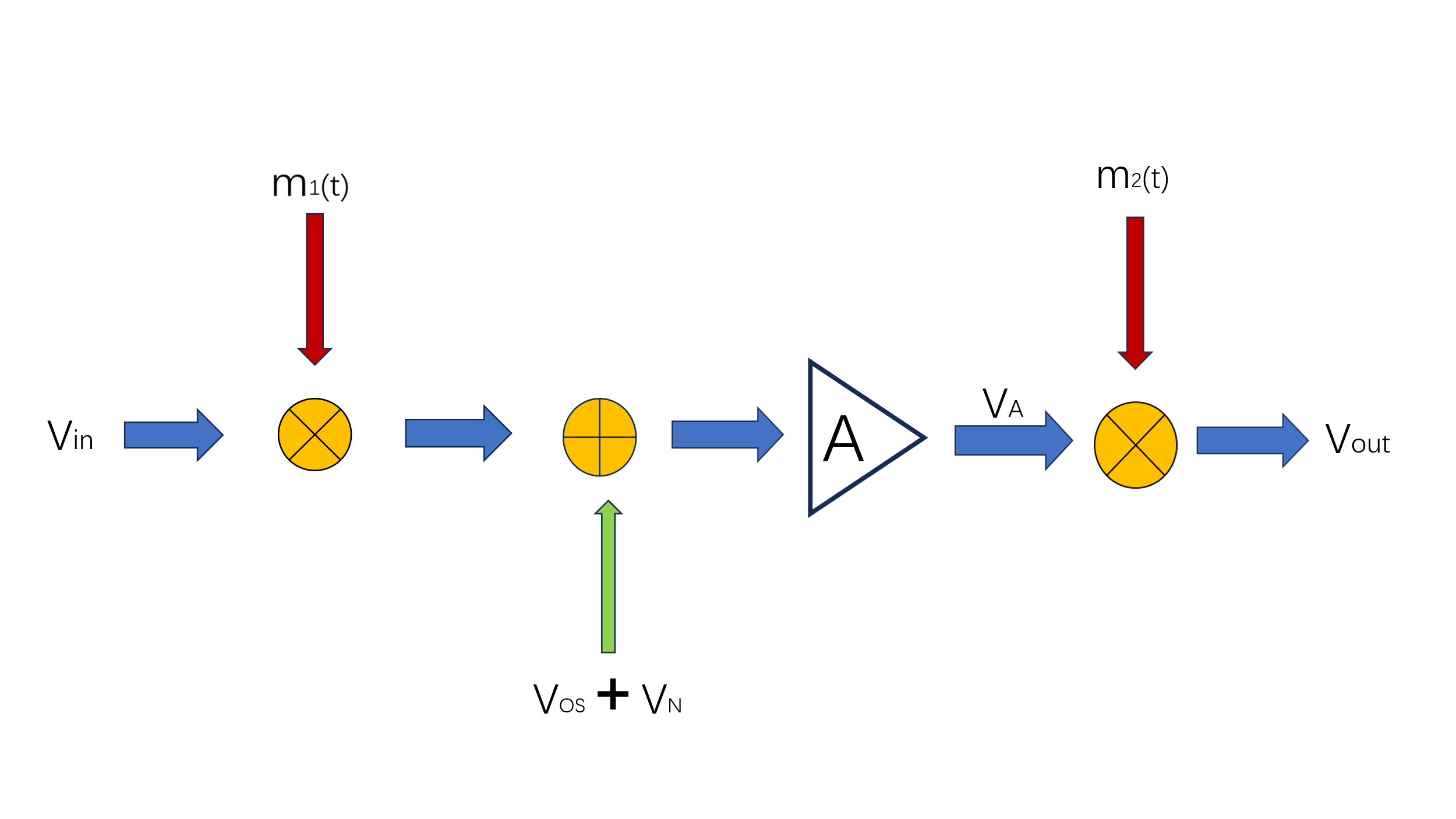
Figure 3. Flow Chart of Chopping Technology
4.2. Auto-zero technology
Automatic zeroing technology is suitable for automatically correcting zero drift in sensors, it determines the baseline for automatically adjusting the equipment, and keep zero output when there is no signal input. Nowadays researchers have designed an automatic zeroing amplifier, they can achieve the input offset voltage of the base through a continuous calibration mechanism to ensure accuracy. Compared to traditional chopper amplifiers, automatic zeroing technology can maintain good performance under AC conditions, and it can provide wider bandwidth and lower output noise [9]. Embedding the calibration mechanism into the amplifier eliminates the need for additional hardware and software for calibration design, the complexity of design and production costs have been reduced. There is also an automatic zero adjustment technology specifically designed to eliminate DC bias and flicker noise, it maintains the offset voltage within a predetermined range by dynamically adjusting the current, use dynamic adjustment of current to maintain offset voltage within a predetermined range, let feedback mechanism for real-time monitoring and adjustment of current, minimizing offset voltage and noise ensures the stability and accuracy of the amplifier [10]. It is not difficult to see from two new circuit designs that automatic zeroing technology is more intelligent, the applicability is also more extensive.
5. Conclusion
This paper summarized the mismatch problem in circuits at three levels, from the device level which includes resistor, capacitor and MOSFET; then the structural level which includes a summary of current mirror structures, differential pair structures in amplifiers and the presence of an out-of-phase voltage Vos; the last level is more advanced mismatch reduction technologies. Overall, the solution to the mismatch is considered at three levels in sequence, use more precise manufacturing processes to manufacture higher precision devices at first, then consider which circuit structures can be used to better minimize the impact of mismatches. Finally, add some compensation methods to the circuit to reduce mismatches and optimize the final result.
Reduce the mismatch plays an important part in improving circuit accuracy. Up to now, people still haven’t very complete system of solutions, so people only solve the problem in their single circuit, not using a molded solution model to reduce the mismatch. It is hoped that a complete solution system can be developed in the future on the basis of an ever improving manufacturing process, making it easier for designers to reduce mismatches from multiple perspectives.
References
[1]. Salonina E A Belyaev Ya V Piatak I M 2020 Modeling the impact of technological process variations on R-2R DAC static characteristics Comput Telecommun Control vol 13 no 3 pp 55–62
[2]. Kang B Liu W T Tang G Q et al 2023 A temperature compensated inductor current detection circuit IEEE Trans Circuits Syst I vol 70 pp 451-459
[3]. Shen Q Wang X Jiang M Chen J He X Zhou H 2024 A capacitive mismatch calibration method for SAR ADCs based on TDC Electron Lett vol 60 no 4 pp 198-205
[4]. Lakshmikumar K R Hadaway R A Copeland M A 1986 Characterisation and modeling of mismatch in MOS transistors for precision analog design IEEE J Solid-State Circuits vol 21 pp 1057-1066
[5]. Pelgrom M J M Duinmaijer A C J Welbers A P G 1989 Matching properties of MOS transistors IEEE J Solid-State Circuits vol 24 no 5 pp 1433-1440
[6]. Datta T Abshire P 2009 Mismatch compensation of CMOS current mirrors using floating-gate transistors IEEE Trans Circuits Syst I vol 56 pp 1823-1826
[7]. Shi N Li Y Y Shen J Ren L W 2023 Design of Low-Offset Input Level of High-Speed Operational Amplifier J Electron Meas Technol vol 23 no 5 pp 050301
[8]. Tang T Park J H Zhang L Ng K A Yoo J 2022 Group-Chopping: An 8-Channel 0.04% Gain Mismatch 2.1 µW 0.017 mm2 Instrumentation Amplifier for Bio-Potential Recording IEEE J Solid-State Circuits vol 16 no 3 pp 361-371
[9]. Kugelstadt T 2005 Auto-zero amplifiers ease the design of high-precision circuits IEEE Analog Appl J vol 2Q pp 19-27
[10]. Safiallah M Danesh A R Pu H Heydari P 2023 A Current-Adjusting Auto-Zeroing Technique for DC-Offset and Flicker-Noise Cancellation IEEE J Solid-State Circuits vol 31 no 12 pp 1950-1959
Cite this article
Ruan,Z. (2024). Reasons and solutions for device mismatch and structural mismatch in electronic circuits. Applied and Computational Engineering,101,207-212.
Data availability
The datasets used and/or analyzed during the current study will be available from the authors upon reasonable request.
Disclaimer/Publisher's Note
The statements, opinions and data contained in all publications are solely those of the individual author(s) and contributor(s) and not of EWA Publishing and/or the editor(s). EWA Publishing and/or the editor(s) disclaim responsibility for any injury to people or property resulting from any ideas, methods, instructions or products referred to in the content.
About volume
Volume title: Proceedings of the 2nd International Conference on Machine Learning and Automation
© 2024 by the author(s). Licensee EWA Publishing, Oxford, UK. This article is an open access article distributed under the terms and
conditions of the Creative Commons Attribution (CC BY) license. Authors who
publish this series agree to the following terms:
1. Authors retain copyright and grant the series right of first publication with the work simultaneously licensed under a Creative Commons
Attribution License that allows others to share the work with an acknowledgment of the work's authorship and initial publication in this
series.
2. Authors are able to enter into separate, additional contractual arrangements for the non-exclusive distribution of the series's published
version of the work (e.g., post it to an institutional repository or publish it in a book), with an acknowledgment of its initial
publication in this series.
3. Authors are permitted and encouraged to post their work online (e.g., in institutional repositories or on their website) prior to and
during the submission process, as it can lead to productive exchanges, as well as earlier and greater citation of published work (See
Open access policy for details).
References
[1]. Salonina E A Belyaev Ya V Piatak I M 2020 Modeling the impact of technological process variations on R-2R DAC static characteristics Comput Telecommun Control vol 13 no 3 pp 55–62
[2]. Kang B Liu W T Tang G Q et al 2023 A temperature compensated inductor current detection circuit IEEE Trans Circuits Syst I vol 70 pp 451-459
[3]. Shen Q Wang X Jiang M Chen J He X Zhou H 2024 A capacitive mismatch calibration method for SAR ADCs based on TDC Electron Lett vol 60 no 4 pp 198-205
[4]. Lakshmikumar K R Hadaway R A Copeland M A 1986 Characterisation and modeling of mismatch in MOS transistors for precision analog design IEEE J Solid-State Circuits vol 21 pp 1057-1066
[5]. Pelgrom M J M Duinmaijer A C J Welbers A P G 1989 Matching properties of MOS transistors IEEE J Solid-State Circuits vol 24 no 5 pp 1433-1440
[6]. Datta T Abshire P 2009 Mismatch compensation of CMOS current mirrors using floating-gate transistors IEEE Trans Circuits Syst I vol 56 pp 1823-1826
[7]. Shi N Li Y Y Shen J Ren L W 2023 Design of Low-Offset Input Level of High-Speed Operational Amplifier J Electron Meas Technol vol 23 no 5 pp 050301
[8]. Tang T Park J H Zhang L Ng K A Yoo J 2022 Group-Chopping: An 8-Channel 0.04% Gain Mismatch 2.1 µW 0.017 mm2 Instrumentation Amplifier for Bio-Potential Recording IEEE J Solid-State Circuits vol 16 no 3 pp 361-371
[9]. Kugelstadt T 2005 Auto-zero amplifiers ease the design of high-precision circuits IEEE Analog Appl J vol 2Q pp 19-27
[10]. Safiallah M Danesh A R Pu H Heydari P 2023 A Current-Adjusting Auto-Zeroing Technique for DC-Offset and Flicker-Noise Cancellation IEEE J Solid-State Circuits vol 31 no 12 pp 1950-1959