


1. Introduction
With the continuous development of integrated circuit technology, high-precision, high-speed, ultra-large-scale digital circuit design and manufacturing become easier and easier, some of the past by the analog circuit to achieve functional modules are gradually replaced by digital circuit modules. However, this does not mean that analog circuits will disappear. on the contrary, with the rapid development of digital circuit technology and the popularity of SOC(System on Chip) design technology, the importance of analog circuit will be further reflected. In analog integrated circuits, an important basic unit circuit, reference source, is widely used. This reference includes reference voltage source and reference current source. The reference source can be used either as a supply voltage or to provide an accurate reference voltage or current for other circuit modules. Moreover, its performance directly affects the performance of the whole circuit. For example, the bias current of the differential pair must be generated according to the reference, since it affects the voltage gain and noise of the circuit. In analog-to-digital converter (ADC) systems, voltage reference sources are also needed to determine the full range of its input or output. The change of reference with temperature and noise will seriously affect the performance of other modules in the circuit and the whole system. Therefore, it is not sensitive to changes in the external environment such as process, supply voltage, and temperature, that is, the stability of the reference source is the main index in the design. If the stability of the reference source is not good, then the system performance is difficult to meet the design requirements.
A bandgap reference voltage source is a circuit that uses the physical characteristics of semiconductor materials to generate stable voltage, and it is the main part of bandgap reference circuit. It is based on the band structure and temperature characteristics of semiconductor materials to achieve high-precision reference voltage output. As a very important unit in analog and hybrid analog circuits, bandgap reference circuit has been paid more and more attention by scholars at home and abroad with the development of integrated circuits and the complication of SOC systems.
The bandgap reference circuit usually consists of a reference voltage source and an error amplifier. The main analysis of this paper is the structure of the bandgap voltage reference and the effect of different improvement schemes.
2. Design Principle of Reference Voltage Source
2.1. Negative temperature coefficient
The reference voltage source uses the bandgap property of semiconductor materials to generate a stable voltage independent of temperature variation, supply fluctuation and process. The research direction tends to get the temperature-independent voltage Vref, that is, to find a positive correlation with temperature and a negative correlation with temperature voltage quantity.
The negative temperature coefficient is generally acted by the base-emitter forward voltage VBE of the PN junction diode, and (1) is the expression of VBE
\( {v_{be}}={v_{T}}{log_{e}}{(\frac{{I_{C}}}{{I_{S}}})}\ \ \ (1) \) ke the derivative of phi of (1)
\( \frac{∂{V_{be}}}{∂T}=\frac{∂{V_{T}}}{∂T}{log_{e}}{(\frac{{I_{C}}}{{I_{S}}})}-\frac{{V_{T}}}{{I_{S}}}\frac{∂{I_{S}}}{∂T}({I_{C}}=constan{t})\ \ \ (2) \)
\( {I_{S}}=b{T^{4+m}}exp{(\frac{-{E_{g}}}{kT})} \) (3)
Substituting (3) into (2) gives
\( \frac{∂{V_{be}}}{∂T}≈\frac{{V_{be}}-(4+m){V_{T}}-{E_{g}}/q}{T} \) (4)
According to (4), Vbe and have negative temperature coefficient (without considering the second-order effect).
Assumptions \( {V_{be}}=750mVT=300°K \) (5)
By substituting the data in (5) into (4)
\( \frac{∂{V_{be}}}{∂T}=-1.5mV/°K \) (6)
According to (6), the negative temperature coefficient is -1.5mV/°K at normal temperature and common voltage
2.2. Positive temperature coefficient
The positive temperature coefficient is generally used as the difference X of the forward voltage between the base and the emitter of two PN junction diodes under different current densities. Generally, there are two ways to change the current density by changing the flow current or changing the current density by changing the area of the PN junction.
First, the way of changing the current density by changing the flow current is introduced.
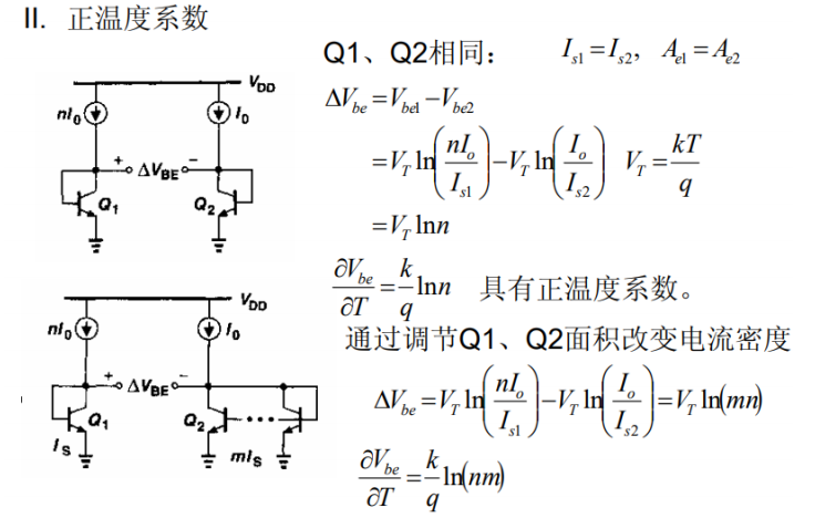
Figure 1. The current flowing through different PN nodes is the same.
Since Q1 and Q2 are exactly the It can be seen from Figure 1 that \( {I_{s1}}={I_{s2}} {A_{e1}}={A_{e2}} \)
X is expressed as (7) and VBE is expressed as (8).
\( Δ{V_{be}}={V_{be1}}-{V_{be2}}\ \ \ (7) \)
\( {v_{be}}={v_{T}}{log_{e}}{(\frac{{I_{C}}}{{I_{S}}})} \) (8)
Substituting (8) into (7) yields (9).
\( Δ{V_{be}}={V_{T}}{log_{e}}{n} \) (9)
\( {V_{T}}=\frac{kT}{q} \) (10)
Then substituting (10) into (9) gives
\( \frac{∂{V_{be}}}{∂T}=\frac{k}{q}{log_{e}}{(nm)} \) (11)
It can be concluded from (11) that the base-emitter forward voltage difference ∆VBE of two PN junction diodes under different current densities has a positive temperature coefficient, where k/q is a constant and is about 0.087mV/°K
As with the above derivation, the final result is simply to add the area ratio ‘m’ to \( {log_{e}}{(n)} \) to obtain (12).
\( \frac{∂{V_{be}}}{∂T}=\frac{k}{q}{log_{e}}{(nm)} \) (12)
2.3. Band gap reference
Finally, the bandgap reference is used to realize the superposition of the two, so as to realize the output voltage not affected by temperature, so it can be assumed that (13)
\( {V_{ref}}={K_{1}}{V_{1}}+{K_{2}}{V_{2}}\ \ \ (13) \)
Combined with the previous derivation, (13) can be changed into (14).
\( {V_{ref}}={α_{1}}{V_{be}}+{α_{2}}{V_{T}}{log_{e}}{n} \) (14)
\( \frac{∂{V_{be}}}{∂T}=-1.5mV/°K \) , \( \frac{∂{V_{T}}}{∂T}=\frac{k}{q}=0.087mV/°K \) (15)
Let \( {α_{1}}=1{ α_{2}}=α \) in (14) and substitute the value in (15) to obtain (16).
\( \frac{∂{V_{ref}}}{∂T}=-1.5+0.087α{log_{e}}{n} \) (16)
So it follows that \( α{log_{e}}{n}≈17.2 \) holds if and only if \( α{log_{e}}{n}≈17.2 \) , in which case \( {V_{ref}} \) equals 0, and the output voltage is not affected by temperature. In general, \( {V_{be}} \) and the size of \( {V_{T}} \) are relatively fixed, as shown in (16), so the value of \( {V_{ref}} \) is generally 1.25V. Part of the optimization of the circuit structure is also devoted to improving the problem that the output voltage is quite stable.
3. Bandgap voltage reference circuit structure principle
3.1. Basic circuit
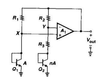
Figure 2. A common basic circuit [1].
It can be seen from Figure 2 that the current of R3 is given by \( \frac{ {V_{BE2}}}{{R_{3}}} \) Since R1 is equal to R2, the currents flowing through them are also the same, so the voltage of R1 is equal to \( {V_{out}}=\frac{{R_{1}}Δ{V_{BE}}}{{R_{3}}}+{V_{BE1}} \) So the output voltage has \( {V_{out}}=\frac{{R_{1}}Δ{V_{BE}}}{{R_{3}}}+{V_{BE1}} \) . Therefore, after satisfying the structure premise R1=R2, if the size of Vout is to be designed, it can be regulated by setting the ratio of R1 and R3, and the power consumption of the whole circuit is determined by R3
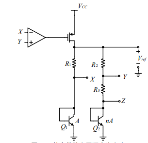
Figure 3. Another common basic circuit.
Figure 3 is another common bandgap reference voltage source structure, and the derivation process is exactly the same as that in Figure 1.
3.2. The current mirror structure is used instead of the operational amplifier
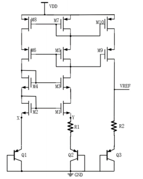
Figure 4. The current mirror structure is used to replace the operational amplifier circuit structure diagram.
As shown in FIG. 4, the structure replaces the opamp with a current mirror structure based on the basic structure and adds a resistor at the output to output the required voltage. Compared with the case of using an op-amp in this structure[2], the structure can directly output positive temperature coefficient current, but using the current mirror structure leads to a decrease in accuracy and is greatly affected by the transistor parameters
3.3. Superimposed current structure
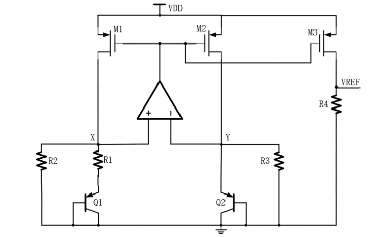
Figure 5. Superimposed current structure(R2=R3 in the circuit,M1 is exactly the same as M2).
This structure is quite different from the above structure. The current with positive and negative temperature coefficients are superimposed to realize the output bandgap reference voltage, and the current flowing through R1 \( \frac{Δ{V_{BE}}}{{R_{1}}} \) [3].
Since M1 is exactly the same as M2, point X is exactly the same as point Y, and since R2=R3, the current flowing through R2 is equal to the current flowing through R3, in figure 5. Therefore, the current flowing through M2 can be obtained by adding \( \frac{Δ{V_{BE}}}{{R_{1}}} \) and \( \frac{{V_{BE2}}}{{R_{3}}} \) .
Therefore, it can be concluded that VREF is \( \frac{{R_{4}}}{{R_{3}}}(\frac{{R_{3}}Δ{V_{BE}}}{{R_{1}}}+{V_{BE2}}) \) As can be seen from it, the advantage of this circuit structure compared with the traditional structure of superposition plus voltage is that the output voltage VREF can be adjusted through R4 to be greater than or less than 1.2V, but the maximum value cannot be greater than VDD-VDS
3.4. Further improvement of the circuit structure for superimposing current
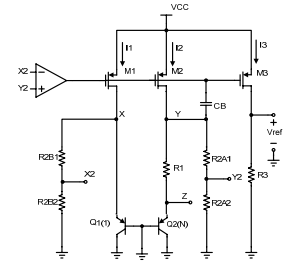
Figure 6. Further improvement of the superposition current circuit structure.
From the analysis of figure. 6 and the previous circuit diagram, VREF can be obtained as \( \frac{{R_{3}}}{{R_{2}}}(\frac{{R_{2}}Δ{V_{BE}}}{{R_{1}}}+{V_{BE2}}) \) . \( \)
Since the voltage drop on R2B1 and R2B2 is VBE1, the voltage to ground of X2 can be obtained as \( \frac{{R_{2B2}}}{{R_{2B1}}+{R_{2B2}}}×{V_{BE1}} \) that the lowest operating voltage is \( \frac{{R_{2B2}}}{{R_{2B2}}+{R_{2B1}}}×{V_{BE1}}+|{V_{thp}}|+2|{V_{DS}}(sat)| \)
It can be concluded that the advantage of this improved structure is that the power supply voltage can be reduced by properly allocating the size of R2A2 and R2B2
4. Advantages of Bandgap Voltage Reference
Through the above derivation, the advantages of bandgap voltage reference can be summarized. Firstly, the bandgap reference through a specific design has temperature stability and is able to generate a stable reference voltage at different temperatures. Second, the bandgap reference voltage source has a strong anti-interference ability to power fluctuations but also has a high precision, and can achieve a high precision reference voltage output usually in a few millivolts or less. Finally, the band-gap reference voltage source also has the characteristics of fast response, and the output voltage can be quickly adjusted to the dynamic input signal.
5. The Characteristics of Bandgap Voltage Reference With Different Structure Improvement and its Application In Different Fields
On the basis of the above common variant bandgap voltage reference structure, many researchers have proposed innovative structures with their own advantages. On the basis of the above superposition current structure, additional transistors are connected in series to realize high-order compensation, which reduces the problem of excessive temperature drift and instability of the traditional bandgap voltage reference [4]. By designing part of the MOS transistors into diode link mode to provide bias voltage, and then making part of the MOS transistors work in the deep linear region as resistors, the positive temperature coefficient voltage is obtained, so that the whole circuit no longer needs resistance, and the error and chip area caused by resistance manufacturing process are reduced [5]. Using the second-order curvature compensation and the structure with temperature drift adjustment [6], only a set of resistors can be used to achieve the adjustment of temperature drift characteristics, which significantly improves the accuracy of the reference voltage and improves the temperature coefficient of the voltage source. There is also a lot of research on improving the accuracy of bandgap reference, For example, by adding a P-type reference resistor with positive temperature coefficient to improve the structure to achieve the effect of second-order temperature compensation [7], and by using a pull-up MOSFET in series with L pull-down MOSFETs [8] to output positive temperature coefficient current, the power consumption is reduced and the accuracy of the bandgap voltage reference is improved. In terms of the power rejection ratio of the bandgap reference voltage source, some people have proposed an improved scheme [9], and designed a circuit structure with low temperature coefficient and high voltage rejection ratio effect. Because of the rapid development of various fields, the demand for different types of chips is also growing rapidly. For chips with high radiation resistance required in the field of spacecraft and satellites, corresponding bandgap voltage reference sources have been designed to resist total dose radiation[10][11]. In the traditional structure, the total dose of radiation will lead to charge entering into the oxide, which will reduce the DC gain and increase the leakage current and base current, resulting in dramatic changes in the characteristics of VBE. Eventually, the positive temperature coefficient becomes larger and the negative temperature coefficient becomes smaller, which cannot be offset by the preset full addition, so that the original set VREF temperature coefficient changes, and the preset effect cannot be achieved. In this paper, the diode link mode is used to generate positive and negative temperature coefficients instead of transistors, because the diode can generate positive and negative temperature coefficients while the base region is less affected by the charge in the oxide layer. There is also a demand for bandgap reference voltage source in the electronic integrated chips of automobiles [12]. According to this paper [13], the circuit structure that meets the working environment conditions of automobiles is proposed. The internal voltage generator provides stable power for the error amplifier, and then the output voltage is detected and controlled by the error amplifier. As can be seen from the above literature, the application range of bandgap reference voltage sources is constantly expanding, and the current research direction is mostly to meet the needs of a certain field's use environment while improving circuit accuracy or stability. This is the future direction of bandgap reference voltage sources.
6. Future Research Directions For Bandgap Voltage Reference Sources
More and more fields begin to put forward the demand for high-performance analog integrated circuits, reference voltage as one of the important components, will be required by more and more complex scenes. Therefore, in the future, the key research direction of bandgap voltage reference will be more inclined to broaden the applicable environment of the voltage source, such as ensuring high precision and controllable temperature coefficient under the power supply voltage in more extreme environments, and adjusting according to the special circumstances of different fields. Circuit design according to different needs is the future research and development direction of bandgap reference voltage source.
This paper presents the basic principles of bandgap voltage reference and illustrates the advantages of these extended circuits from the basic circuit to various representative extended circuits compared to the original circuit. At the same time, several improvement directions and corresponding examples of the bandgap voltage reference structure are introduced, such as more compensation means, lower power consumption and replacing the existing structure with another structure to achieve some goals. Several kinds of chips used in specific fields are introduced, and their principles and advantages are briefly introduced.
Therefore, through the above discussion and the analysis of the literature, it can be concluded that there are still many challenges in the future bandgap voltage reference, such as how to ensure the normal operation of the circuit in high temperature or low temperature environment, how to improve the temperature coefficient of the circuit to improve the output current accuracy based on the previous circuit, how to reduce the requirements for the process, how to control the power consumption according to the demand, and how to reduce the temperature coefficient of the circuit. Cost, voltage rejection ratio and other indicators. These are the challenges that future bandgap benchmark circuits will encounter in practical applications in various neighborhoods.
For these challenges, some researchers have begun to study them by adding first-order and second-order temperature compensation circuits to reduce the temperature coefficient and improve the output voltage accuracy [2]. In addition, the use of special resistors to achieve temperature compensation in low temperature environment to achieve low temperature coefficient voltage output [13] to improve the current situation that many circuits are demanding on temperature. These examples can prove that the current research direction of bandgap voltage reference is to improve the output accuracy and broaden the applicable environment. Of course, to do these two things is not only to work on the temperature and aspects, in order to output a variety of voltage values, better adapt to the situation that different parts of the chip need a variety of different sizes of voltage at the same time, there are also special studies [14].
In conclusion, now almost all industries are inseparable from the integrated circuit, and as an important part of the integrated circuit, the bandgap benchmark circuit part is also very important. In order to comply with such a development trend, the bandgap reference voltage source has also begun to change and improve. By summarizing and comparing the advantages and disadvantages of the old structure and then improving the structure on this basis, the effect is achieved by adding circuit structures such as compensation circuits. This will also be the development trend of bandgap benchmark circuits in the future, through the improvement of the structure to adapt to the different needs in the market now.
References
[1]. Li Xin, Gao Mengzhen, Yang Shenglin. A new type of bandgap reference with curvature compensation [J]. Materials and electronic components, lancet, 2024 (7) : 878-883. The DOI: 10.14106 / j.carol carroll nki. 1001-2028.2024.1596.7.
[2]. Wang Xinyu, Jiang Dandan, Yan Zhe. A high-precision low-power bandgap voltage reference source design [J]. Journal of chengdu university of information engineering, 2024, 33 (5) : 6, 560-566. The DOI: 10.16836 / j.carol carroll nki jcuit. 2024.05.007.Zou X Zhang Y Wu X, Cong G 2024 A High Stability Bandgap Reference Circuit without Amplifier Structure Proc 3rd Int Conf. on Energy Power and Electrical Technology (ICEPET) pp 968-971
[3]. Kong Luping. Design of Voltage Reference in 12bit 50MSPS Pipeline ADC [D]. Southeast University,2017.
[4]. Cheng L, Zhao Z, Hou W 2019 A Bandgap Reference Circuit without Resistance Structure Shanxi Electron. Technol. (05) pp 29-31+49
[5]. Li J Zhang H B Li J et al 2019 With a temperature drift of the second-order curvature compensation reference source circuit J Electron Encapsul 12 (11) pp 26-30
[6]. Han Q, Wang C, Zhong D, et al 2024 A with laser repair of the high precision band gap reference voltage source Semicond Technol pp 1-6
[7]. Lin Z 2024 A 11.5nW CMOS bandgap voltage and current reference Proc IEEE 4th Int Conf. on Electron Technol Commun. and Inf (ICETCI) pp 828-833
[8]. Ye M Tong M S 2023 A Novel Bandgap Voltage Reference Source with High Power Supply Rejection Proc. Photonics Electromagnetics Res Symp (PIERS) pp 1501-1507
[9]. Hu Y Wang Z Yang Y et al 2022 A bandgap voltage reference source resistance to total dose radiation J Microelectron 52 (4) pp 562-565
[10]. Traversi G Gaioni L Ballabriga R Ceresa D Michelis S 2022 Design of a Radiation-Tolerant Bandgap Voltage Reference for HEP applications Proc IEEE Nucl Sci Symp and Med Imag Conf pp 1-3
[11]. Xu W, Zhang X, Chuai R 2021 Design of a Voltage Regulator Chip for High-power Automobile Generator Microprocessor 42 (04) pp 21-24
[12]. Kostanyan H T Kostanyan H T Hayrapetyan A K Petrosyan A S Petrosyan G A Marukhyan D K 2019 5V wide supply voltage bandgap reference for automotive applications Proc IEEE 39th Int Conf on Electron and Nanotech pp 229-232
[13]. Lou Yichun, DU Chenggang, MIN Rui, et al. A 3 x 10⁻⁶ / ℃ ultra-low temperature drift bandgap reference source [J]. Journal of semiconductor technology, 2024,49 (8) : 742-748. The DOI: 10.13290 / j.carol carroll nki BDTJS. 2024.08.008.
[14]. LI Siyuan, LI Yajun, Zhang Youtao, et al. A wide range of input high PSR bandgap reference circuit design [J]. Journal of electronic technology applications, 2024, 50 (04) : 38 and 43. DOI: 10.16157 / j.i SSN. 0258-7998.234751.
Cite this article
Han,S. (2024). Research on Design Method and Application of Bandgap Voltage Reference. Applied and Computational Engineering,107,92-100.
Data availability
The datasets used and/or analyzed during the current study will be available from the authors upon reasonable request.
Disclaimer/Publisher's Note
The statements, opinions and data contained in all publications are solely those of the individual author(s) and contributor(s) and not of EWA Publishing and/or the editor(s). EWA Publishing and/or the editor(s) disclaim responsibility for any injury to people or property resulting from any ideas, methods, instructions or products referred to in the content.
About volume
Volume title: Proceedings of the 2nd International Conference on Machine Learning and Automation
© 2024 by the author(s). Licensee EWA Publishing, Oxford, UK. This article is an open access article distributed under the terms and
conditions of the Creative Commons Attribution (CC BY) license. Authors who
publish this series agree to the following terms:
1. Authors retain copyright and grant the series right of first publication with the work simultaneously licensed under a Creative Commons
Attribution License that allows others to share the work with an acknowledgment of the work's authorship and initial publication in this
series.
2. Authors are able to enter into separate, additional contractual arrangements for the non-exclusive distribution of the series's published
version of the work (e.g., post it to an institutional repository or publish it in a book), with an acknowledgment of its initial
publication in this series.
3. Authors are permitted and encouraged to post their work online (e.g., in institutional repositories or on their website) prior to and
during the submission process, as it can lead to productive exchanges, as well as earlier and greater citation of published work (See
Open access policy for details).
References
[1]. Li Xin, Gao Mengzhen, Yang Shenglin. A new type of bandgap reference with curvature compensation [J]. Materials and electronic components, lancet, 2024 (7) : 878-883. The DOI: 10.14106 / j.carol carroll nki. 1001-2028.2024.1596.7.
[2]. Wang Xinyu, Jiang Dandan, Yan Zhe. A high-precision low-power bandgap voltage reference source design [J]. Journal of chengdu university of information engineering, 2024, 33 (5) : 6, 560-566. The DOI: 10.16836 / j.carol carroll nki jcuit. 2024.05.007.Zou X Zhang Y Wu X, Cong G 2024 A High Stability Bandgap Reference Circuit without Amplifier Structure Proc 3rd Int Conf. on Energy Power and Electrical Technology (ICEPET) pp 968-971
[3]. Kong Luping. Design of Voltage Reference in 12bit 50MSPS Pipeline ADC [D]. Southeast University,2017.
[4]. Cheng L, Zhao Z, Hou W 2019 A Bandgap Reference Circuit without Resistance Structure Shanxi Electron. Technol. (05) pp 29-31+49
[5]. Li J Zhang H B Li J et al 2019 With a temperature drift of the second-order curvature compensation reference source circuit J Electron Encapsul 12 (11) pp 26-30
[6]. Han Q, Wang C, Zhong D, et al 2024 A with laser repair of the high precision band gap reference voltage source Semicond Technol pp 1-6
[7]. Lin Z 2024 A 11.5nW CMOS bandgap voltage and current reference Proc IEEE 4th Int Conf. on Electron Technol Commun. and Inf (ICETCI) pp 828-833
[8]. Ye M Tong M S 2023 A Novel Bandgap Voltage Reference Source with High Power Supply Rejection Proc. Photonics Electromagnetics Res Symp (PIERS) pp 1501-1507
[9]. Hu Y Wang Z Yang Y et al 2022 A bandgap voltage reference source resistance to total dose radiation J Microelectron 52 (4) pp 562-565
[10]. Traversi G Gaioni L Ballabriga R Ceresa D Michelis S 2022 Design of a Radiation-Tolerant Bandgap Voltage Reference for HEP applications Proc IEEE Nucl Sci Symp and Med Imag Conf pp 1-3
[11]. Xu W, Zhang X, Chuai R 2021 Design of a Voltage Regulator Chip for High-power Automobile Generator Microprocessor 42 (04) pp 21-24
[12]. Kostanyan H T Kostanyan H T Hayrapetyan A K Petrosyan A S Petrosyan G A Marukhyan D K 2019 5V wide supply voltage bandgap reference for automotive applications Proc IEEE 39th Int Conf on Electron and Nanotech pp 229-232
[13]. Lou Yichun, DU Chenggang, MIN Rui, et al. A 3 x 10⁻⁶ / ℃ ultra-low temperature drift bandgap reference source [J]. Journal of semiconductor technology, 2024,49 (8) : 742-748. The DOI: 10.13290 / j.carol carroll nki BDTJS. 2024.08.008.
[14]. LI Siyuan, LI Yajun, Zhang Youtao, et al. A wide range of input high PSR bandgap reference circuit design [J]. Journal of electronic technology applications, 2024, 50 (04) : 38 and 43. DOI: 10.16157 / j.i SSN. 0258-7998.234751.