


1. Introduction
An analog-to-digital converter (ADC) is an electronic device that converts external analog signals into digital signals that can be recognized and utilized by a computer. Digital signals are easier to process, store, and transmit with high accuracy compared to analog signals, which broadens their application across communication systems, audio and video processing, sensor data acquisition, and numerous other fields. The development history of ADC can be traced back to the mid-20th century, when the rapid development of digital technology increased the demand for converting analog signals into digital signals. Nowadays, analog-to-digital converters play an indispensable and important role in communication systems, sensors, industrial control, medical instruments, and other fields. However, the research and development of ADC, especially high-performance ADC, is currently a bottleneck field in China, where there is a significant gap compared to foreign countries. Furthermore, high-performance ADC chips are often subject to export restrictions from other countries [1]. Therefore, it is essential to draw experience from foreign research to promote the development of ADC domestically.
Based on existing literature and data research, this article first introduces several commonly used ADC structures, including Flash ADC, Sigma Delta( \( Σ-Δ \) ) ADC, and Sequential Approximation (SAR) ADC, exploring their advantages, disadvantages, application areas, and development directions. Secondly, this article compares the performance and design ideas of ADC research in China and abroad from three aspects: high speed, high precision, and low power consumption. This comparison highlights significant gaps and differences between China and foreign countries in three aspects. Finally, this article analyzes the future development direction of the ADC field, with an emphasis on research into new ADC designs as a core focus for future study. The purpose of this study is to clarify the differences between domestic ADCs and foreign ADCs and provide some directions for future extensive research on ADCs. The research analysis in this article can better understand the weak aspects of ADC research in China and underscores the need for strengthened efforts in these areas.
2. Mainstream ADC architecture
Since their inception, analog-to-digital converters (ADCs) have developed across a range of architectures, including Flash ADC, Pipeline ADC, TI ADC, \( Σ-Δ \) ADC, Sequential Approximation (SAR) ADC, Reconfigure ADC, etc. These architectures have their own characteristics, advantages, disadvantages, and applicable fields. This article mainly introduces three commonly used ADC architectures: Flash ADC, \( Σ-Δ \) ADC, and SAR ADC.
2.1. Flash ADC
Flash ADC is a high-speed ADC with an extremely simple structure. This converter can directly convert the input analog voltage into the digital signal output without the need for intermediate variables.
The structure of Flash ADC is shown in Figure 1, which mainly consists of three parts: voltage comparator, code converter, and register. In the voltage comparator, the resistor chain divides the reference voltage, and the resulting voltage levels are connected to the input terminal of the voltage comparator as a reference for comparison. Simultaneously, the input analog voltage is applied to the other input terminal of the comparator. The comparator compares the analog input voltage with the reference point and obtains a binary code. This binary code is subsequently processed by the code converter to yield the digital signal, which is then stored in the register. Finally, the register outputs the converted digital signal after all analog signals have been processed and compared.
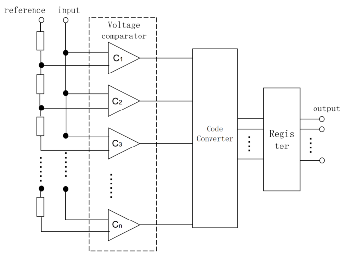
Figure 1. Schematic diagram of Flash ADC structure
The advantage of Flash ADC is that it can directly compare the input signal with the reference voltage, thus allowing for a very high conversion rate. However, as the accuracy of Flash ADC increases, the number of its comparators and resistors rises geometrically. For example, an N-bit digital output requires \( {2^{N}} \) matching resistors, significantly increasing its power consumption. As a result, Flash ADC is limited in achieving very high accuracy due to the high power demands.
2.2. \( Σ-Δ \) ADC
\( Σ-Δ \) ADC is a typical high-precision ADC. It reduces the impact of noise and improves conversion accuracy through techniques such as oversampling and noise shaping.
\( Σ-Δ \) ADC has three processes: oversampling, \( Σ-Δ \) modulation, and digital filtering, as shown in Figure 2. The ADC first samples the input signal at a rate multiple times higher than the highest frequency component of the input signal, a process known as oversampling. Next, the oversampled signal is passed through a \( Σ-Δ \) modulator, which contains an integrator that can accumulate the input signal and compare it with a reference voltage through a comparator to generate a binary output. During this stage, low-frequency signals are retained, while noise is shifted to the high-frequency range — a process called noise shaping. After that, the \( Σ-Δ \) modulator output data stream will pass through a digital low-pass filter, which extracts useful signals from high-frequency noise and converts them to a lower sampling rate, thus improving the resolution. Finally, a digital signal with a lower sampling rate and higher resolution is obtained.
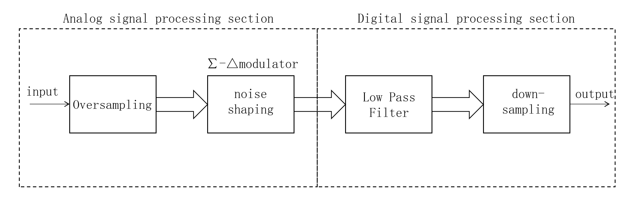
Figure 2. Schematic diagram of \( Σ-Δ \) ADC structure
Due to its relatively straightforward circuitry and high conversion accuracy, ΣΔ ADC is widely used in fields such as audio systems, medical devices, and precision instruments. However, ΣΔ ADC is limited by a slower conversion rate, typically achieving less than 100,000 conversions per second, which remains its primary disadvantage.
2.3. SAR ADC
SAR ADC has become the most widely used ADC at present due to its advantages of low power consumption, small area, and simple structure. SAR ADC adopts a feedback comparison structure, sequentially changing the digital quantity in a sequential comparison manner to obtain the correct results.
The SAR ADC sequentially compares the input signal with the reference voltage value generated by the digital to analog converter, producing output from the highest bit to the lowest bit. Figure 3 illustrates its structure. The process begins by taking an initial digital value and feeding it into the DAC to generate a corresponding analog voltage. After this, this analog voltage is compared with the actual input analog signal. If the two are not equal, the digital value is adjusted, and the comparison is repeated until the generated analog signal precisely matches the input signal. This process continues sequentially until the full digital output is achieved.
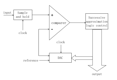
Figure 3. Schematic diagram of SAR ADC structure
The biggest feature of SAR ADC is its extremely low power consumption, which is at the \( μ \) W level. In recent years, many studies have been devoted to improving the accuracy and speed of SAR ADCs, making them applicable to more fields. For example, a hybrid design of SAR ADC and Flash ADC can increase the sampling rate to 100MS/s, and a hybrid RC DAC module can be used in SAR ADC to reduce the number of capacitors that increase with the number of digital signal bits, thereby improving accuracy to 12 bits [2-3].
3. Development of ADC at home and abroad
While ADC technology is a crucial focus in national development, domestic advancements still lag behind those of foreign counterparts due to a later start in the field. This article compares the latest research in three key areas of ADC development: high speed, high precision, and low power consumption, in the hope that some domestic research can benefit from the comparison with foreign research.
3.1. High speed ADC
Firstly, the study compares the current research on high-speed ADCs at home and abroad from a performance perspective. The ADCs developed domestically are mostly at the MS/s level, and there are also GS/s level speeds [2, 4, 5]. In contrast, the high-speed ADCs developed abroad are mostly at the GS/s level, and the ADC designed by Amy Whitcombe and others can even achieve a conversion rate of 40GS/s. This disparity underscores the significant gap between domestic and foreign high-speed ADC capabilities [6-8].
Next, the study compares the methods and technologies for improving ADC conversion rates at home and abroad in recent years. The mainstream methods currently used in China are as follows: the ADC designed by Huang Zheng uses a pipeline architecture that segments the input signal in sequence from high to low, converting it into a digital signal. This architecture has a relatively simple structure and can improve the conversion rate [4]. The design by Zhang Hang's team is an integral type ADC, which is controlled by the cooperation of a microcontroller and CPLD. At the end of the integration, the residual voltage of the integrator is measured using the on-chip ADC of the microcontroller, greatly improving the conversion rate [5]. Tian Ruiqian’s team designed a hybrid architecture ADC that combines SAR ADC and Flash ADC, utilizing the parallel advantage of Flash ADC to improve speed [2].
By comparison, foreign researchers have focused predominantly on time-interleaving (TI) technology for high-speed ADCs. Amy Whitcombe uses a single high-speed voltage time converter (VTC) as the high bandwidth sampling buffer for four TI SAR ADCs [6]. This hybrid architecture that combines VTC is very suitable for time interleaving, improving the efficiency of time interleaving and thus increasing speed. Siji Huang, on the other hand, uses a centralized sampling front-end with a single S/H network, which eliminates timing bias and eliminates the need for calibration, improving efficiency and speed [7]. Another design by Amy Whitcombe’s team integrates a hybrid voltage and time (V+T) ADC, which combines the speed advantage of time-domain conversion and simplifies the time interleaving process through the V+T architecture, greatly improving the conversion speed [8].
From two aspects of comparison, there is a significant gap in the performance of domestic high-speed ADCs compared to foreign ones. While time-interleaving technology is widely used abroad to enhance speed, it remains relatively rare in domestic research, indicating an opportunity for increased focus on this method within China to improve ADC conversion rates.
3.2. High precision ADC
From the current research on high-precision ADC performance both domestically and internationally, there is not much difference in resolution between the ADCs developed domestically and internationally. The resolution of high-precision ADCs developed domestically is roughly 10-30 bits [9-11]. However, the resolution range of foreign ADCs is roughly 10-20 bits [3, 5, 12]. Although the performance gap is minimal, the technologies employed differ significantly.
To enhance ADC conversion accuracy, domestic research has focused primarily on noise reduction techniques. For example, Tan Peitao mainly uses oversampling and noise shaping techniques to remove internal noise from signals and then uses digital filtering techniques to remove external noise [9]. The Zoom ADC used by Zhang Lu is a hybrid architecture ADC that combines the noise reduction advantages of SAR ADC with DEM and correlated double sampling techniques to reduce noise and significantly improve the conversion accuracy of ADC [10]. Zhao Zhuang and colleagues used a novel second-order passive lossless integration loop filter for noise shaping, effectively minimizing noise impact and enabling high-precision conversion [11].
However, there are more technologies adopted abroad. Mi Ji Go has improved the SAR ADC to achieve high precision, which reduces the capacitor count that typically increases with precision, resulting in lower production complexity, power consumption, and device area [3]. Matheus B. S. Carvalho et al. improved the SAR ADC by using a common mode voltage based method to enhance the comparison accuracy between the analog signal obtained by the analog-to-digital converter and the input signal, thereby improving the accuracy of the SAR ADC output signal [12].
In summary, while domestic and foreign high-precision ADCs show similar performance levels, the technological approaches differ. Domestically, further noise reduction techniques can help minimize internal and external noise within ADCs, and modifying SAR ADC designs, as seen internationally, could enhance both conversion rates and accuracy in this widely-used ADC architecture.
3.3. Low power ADC
In terms of low-power ADCs, the lowest power consumption achievable both domestically and internationally is at the W level [10, 13, 14]. Internationally, ADC power consumption often reaches the mW level, demonstrating similar advancements in low-power ADC development[12, 15, 16].
Domestically, Ye Weicheng is modifying the SAR ADC, which uses a fully dynamic comparator, significantly reducing the static power consumption of the comparator; using segmented capacitive analog-to-digital converters to reduce power consumption caused by large area [14]. Zhang Lu uses a hybrid Zoom architecture, which effectively maintains the low-power characteristics of the SAR ADC it contains [10]. Feng Rui's design for CMOS image sensors uses segmented capacitive analog-to-digital converters to reduce the area and power consumption of the analog-to-digital converter array, thereby reducing the total power consumption of the ADC [15]. Internationally, Matheus B. S. Carvalho et al. used methods such as lock-in dynamic comparators to prevent ADC from generating static power consumption [12]. The method used by Tejas MP is also an improved comparator [15]. The dynamic latch comparator has been improved by adding controllable PMOS transistors and using capacitive elements, reducing power consumption. Amit Shohal adopts a pipeline ADC and uses advanced transistor languages such as Verilog-A to reduce the inherent power loss of pipeline ADC. Compared with traditional 180nm technology, the power consumption is reduced to 0.12W, which is four times lower [16].
From the comparison, not much difference can be found in performance between low-power ADCs at home and abroad, particularly in SAR ADC modifications. To further minimize power consumption, China could explore simplifying SAR ADC structure or employing hybrid designs to enhance efficiency.
4. Future development trends
With wide applications and global significance, ADC has substantial development prospects. At present, the future development direction of ADC is multifaceted, such as new ADCs with better performance, intelligent ADCs using mechanical learning, ADCs that can adapt to extreme environments such as low-temperature environments, etc. [17-20]. This article discusses the new type of ADC that has emerged and is widely studied at present. The new ADCs are mainly divided into two categories: non-traditional new architectures and hybrid architectures.
Among novel architecture ADC, reconfigurable ADC is one of the most widely studied ADCs [21]. The basic idea of reconfigurable ADC is to dynamically change the structure and parameters of the system in different application scenarios, so that the system can maintain the highest possible performance and efficiency in various scenarios. Photon ADC is another type of ADC that has attracted much attention, and photon based ADCs can greatly outperform electronic ADCs in terms of speed and resolution [22]. However, the problem with the new architecture ADC is that the technology is not mature enough to be widely applied in practical engineering.
Hybrid architecture ADCs encompass various types, such as Flash SAR ADC, hybrid time-voltage domain ADC, TI SAR ADC, and Zoom ADC [2, 6, 7, 10]. The core idea of hybrid architecture ADC is to combine two or even multiple ADC architectures together to leverage their respective strengths. Many of these hybrid architecture ADCs are based on SAR ADCs. However, achieving an effective hybrid that retains the advantages of its components remains challenging, resulting in relatively few high-performance hybrid ADCs.
5. Conclusion
This article summarizes the development of ADC from three aspects: mainstream ADC structures, domestic and foreign research comparisons, and future development trends. The first part introduces three classic ADC structures: Flash ADC, \( Σ-Δ \) ADC, and SAR ADC. Each of the three structures has its own characteristics, among which SAR ADC is the most widely used. The second part compares domestic and foreign research from three perspectives: high speed, high precision, and low power consumption, revealing a clear gap in high-speed ADCs, while high-precision and low-power ADCs show smaller performance disparities, though foreign methods offer useful insights. The third part discusses the future development direction of ADCs, with a focus on introducing new ADCs, including new architecture ADCs and hybrid architecture ADCs. Future ADC development will likely focus on new and hybrid architectures, such as reconfigurable ADCs, to meet evolving demands and environmental challenges.
Acknowledgment
Firstly, I would like to express my deepest gratitude to my university professors for providing me with valuable guidance at every stage of writing this paper. In addition, I would like to thank my friends and family for their encouragement and support. Without their help, I would not have been able to complete my paper.
References
[1]. Qi Xiaohu. 2023. Research and Design of Key Technologies for High Precision Analog to Digital Converter [D]. Sichuan: University of Electronic Science and Technology of China.
[2]. Tian Ruiqian, Song Shuxiang, Zhao Yuan, etc. 2023. Design of a 12 bit 100 MS/s Flash SAR Hybrid Analog to Digital Converter [J]. Radio Engineering, 53 (6): 1421-1429.
[3]. M. -J. Go et al., 2023. "A 12-bit 3-MS/s Synchronous SAR ADC With a Hybrid RC DAC," 2023 20th International SoC Design Conference (ISOCC), Jeju, Korea, Republic of, pp. 191-192.
[4]. Huang Zheng, Cai Mengye, Jiang Yanfeng. 2024. An 11 bit pipeline high-speed analog-to-digital converter [J]. Semiconductor Technology, 49 (6): 561-568.
[5]. Zhang Hang, Li Liusheng, Luo Qiren, etc. 2024. Design of 7-and-a-half bit AD converter based on improved multi skew III technology [J]. Environmental Technology, 42 (5): 200-204.
[6]. Whitcombe, A., Lee, C. C., Thekkumpate, A. B. K., Kundu, S., Timbadiya, J., Agrawal, A., ... & Hull, C. (2023). A VTC/TDC-Assisted 4× Interleaved 3.8 GS/s 7b 6.0 mW SAR ADC With 13 GHz ERBW. IEEE Journal of Solid-State Circuits, 58(4), 972-982.
[7]. Huang, S., Basak, D., Chen, Y., Huang, Q., Fan, Y., & Yuan, J. (2024). An Efficient 1.4-GS/s 10-bit Timing-Skew-Free Time-Interleaved SAR ADC With a Centralized Sampling Frontend. IEEE Transactions on Very Large Scale Integration (VLSI) Systems.
[8]. Whitcombe, A., Kundu, S., Chandrakumar, H., Agrawal, A., Brown, T., Callender, S., ... & Pellerano, S. (2024). A 7b 76mW 40GS/s Hybrid Voltage/Time-Domain ADC With Common-Mode Input Tracking. IEEE Solid-State Circuits Letters.
[9]. Tan Peitao. 2023. Research and Design of High Precision 100Mbps Sampling Rate Pipeline Sequential Approximation Analog to Digital Converter [D]. Sichuan: University of Electronic Science and Technology of China.
[10]. Zhang Lu. 2023. High precision and low-power Zoom type analog-to-digital converter based on dynamic element matching [D]. Liaoning: Dalian University of Technology.
[11]. Zhao Zhuang, Fu Yunhao, Gu Yanxue, etc. 2024. Design of high-precision and low-power noise shaping SAR ADC [J]. Journal of Jilin University (Information Science Edition), 42 (2): 226-231.
[12]. M. B. S. Carvalho, T. C. dos Santos, R. D. P. de Oliveira, A. G. 2024. Girardi and P. C. C. de Aguirre, "A Low-Power 10-Bit VCM-Based SAR ADC with 15.4-fJ/conv in 65-NM CMOS," 2024 Argentine Conference on Electronics (CAE), Bahía Blanca, Argentina, pp. 109-114.
[13]. Ye Weicheng. 2023. Research on Low Power SAR ADC Based on Digital Error Correction [D]. Liaoning: Dalian University of Technology.
[14]. Feng Rui. 2023. Research on Sequential Approximation Analog to Digital Converter for CMOS Image Sensor [D]. Sichuan: University of Electronic Science and Technology of China.
[15]. T. M P and Venkateshappa, 2024. "Design and Optimization of a Low-Power Comparator for a 10-Bit Successive Approximation Register (SAR) Analog-to-Digital Converter (ADC) for General-Purpose Applications," 2024 International Conference on Intelligent and Innovative Technologies in Computing, Electrical and Electronics (IITCEE), Bangalore, India, pp. 1-4.
[16]. A. Shohal and J. Kaur, 2024. "Verilog-A Based 8-Bit Pipeline ADC Tailored for Low Power Performance and High-Speed Operation in 90 nm Technology," 2024 International Conference on Electronics, Computing, Communication and Control Technology (ICECCC), Bengaluru, India, pp. 1-5.
[17]. Hou Linjie. 2023. Design and Implementation of ADC Parameter Estimation Algorithm Based on Machine Learning [D]. Sichuan: University of Electronic Science and Technology of China.
[18]. S. P. Bhanushali and A. Sanyal, 2024. "Enhancing Performance of SAR ADC through Supervised Machine Learning," 2024 IEEE International Symposium on Circuits and Systems (ISCAS), Singapore, Singapore, pp. 1-5.
[19]. Wen Mingjie. 2023. Research and Implementation of Low Temperature Analog to Digital Converter for Silicon based Quantum Computers [D]. Anhui: University of Science and Technology of China.
[20]. E. Worsey, Q. Tang, M. B. Krishnan, M. Kumar Kulsreshath and D. Pamunuwa, 2024. "Nanoelectromechanical analog-to-digital converter for low power and harsh environments," 2024 IEEE International Symposium on Circuits and Systems (ISCAS), Singapore, Singapore, pp. 1-5.
[21]. Jie Lu. 2023. Overview of Reconfigurable Analog to Digital Converter Technology [J]. Micro Nano Electronics and Intelligent Manufacturing, 5 (2): 1-7.
[22]. Deakin, C., & Liu, Z. (2023). Energy Efficiency Bounds for Photonic Analog to Digital Converters. Journal of Lightwave Technology.
Cite this article
Wang,J. (2024). Overview of Structure Design and Development of Analog to Digital Converter. Applied and Computational Engineering,114,32-39.
Data availability
The datasets used and/or analyzed during the current study will be available from the authors upon reasonable request.
Disclaimer/Publisher's Note
The statements, opinions and data contained in all publications are solely those of the individual author(s) and contributor(s) and not of EWA Publishing and/or the editor(s). EWA Publishing and/or the editor(s) disclaim responsibility for any injury to people or property resulting from any ideas, methods, instructions or products referred to in the content.
About volume
Volume title: Proceedings of the 2nd International Conference on Machine Learning and Automation
© 2024 by the author(s). Licensee EWA Publishing, Oxford, UK. This article is an open access article distributed under the terms and
conditions of the Creative Commons Attribution (CC BY) license. Authors who
publish this series agree to the following terms:
1. Authors retain copyright and grant the series right of first publication with the work simultaneously licensed under a Creative Commons
Attribution License that allows others to share the work with an acknowledgment of the work's authorship and initial publication in this
series.
2. Authors are able to enter into separate, additional contractual arrangements for the non-exclusive distribution of the series's published
version of the work (e.g., post it to an institutional repository or publish it in a book), with an acknowledgment of its initial
publication in this series.
3. Authors are permitted and encouraged to post their work online (e.g., in institutional repositories or on their website) prior to and
during the submission process, as it can lead to productive exchanges, as well as earlier and greater citation of published work (See
Open access policy for details).
References
[1]. Qi Xiaohu. 2023. Research and Design of Key Technologies for High Precision Analog to Digital Converter [D]. Sichuan: University of Electronic Science and Technology of China.
[2]. Tian Ruiqian, Song Shuxiang, Zhao Yuan, etc. 2023. Design of a 12 bit 100 MS/s Flash SAR Hybrid Analog to Digital Converter [J]. Radio Engineering, 53 (6): 1421-1429.
[3]. M. -J. Go et al., 2023. "A 12-bit 3-MS/s Synchronous SAR ADC With a Hybrid RC DAC," 2023 20th International SoC Design Conference (ISOCC), Jeju, Korea, Republic of, pp. 191-192.
[4]. Huang Zheng, Cai Mengye, Jiang Yanfeng. 2024. An 11 bit pipeline high-speed analog-to-digital converter [J]. Semiconductor Technology, 49 (6): 561-568.
[5]. Zhang Hang, Li Liusheng, Luo Qiren, etc. 2024. Design of 7-and-a-half bit AD converter based on improved multi skew III technology [J]. Environmental Technology, 42 (5): 200-204.
[6]. Whitcombe, A., Lee, C. C., Thekkumpate, A. B. K., Kundu, S., Timbadiya, J., Agrawal, A., ... & Hull, C. (2023). A VTC/TDC-Assisted 4× Interleaved 3.8 GS/s 7b 6.0 mW SAR ADC With 13 GHz ERBW. IEEE Journal of Solid-State Circuits, 58(4), 972-982.
[7]. Huang, S., Basak, D., Chen, Y., Huang, Q., Fan, Y., & Yuan, J. (2024). An Efficient 1.4-GS/s 10-bit Timing-Skew-Free Time-Interleaved SAR ADC With a Centralized Sampling Frontend. IEEE Transactions on Very Large Scale Integration (VLSI) Systems.
[8]. Whitcombe, A., Kundu, S., Chandrakumar, H., Agrawal, A., Brown, T., Callender, S., ... & Pellerano, S. (2024). A 7b 76mW 40GS/s Hybrid Voltage/Time-Domain ADC With Common-Mode Input Tracking. IEEE Solid-State Circuits Letters.
[9]. Tan Peitao. 2023. Research and Design of High Precision 100Mbps Sampling Rate Pipeline Sequential Approximation Analog to Digital Converter [D]. Sichuan: University of Electronic Science and Technology of China.
[10]. Zhang Lu. 2023. High precision and low-power Zoom type analog-to-digital converter based on dynamic element matching [D]. Liaoning: Dalian University of Technology.
[11]. Zhao Zhuang, Fu Yunhao, Gu Yanxue, etc. 2024. Design of high-precision and low-power noise shaping SAR ADC [J]. Journal of Jilin University (Information Science Edition), 42 (2): 226-231.
[12]. M. B. S. Carvalho, T. C. dos Santos, R. D. P. de Oliveira, A. G. 2024. Girardi and P. C. C. de Aguirre, "A Low-Power 10-Bit VCM-Based SAR ADC with 15.4-fJ/conv in 65-NM CMOS," 2024 Argentine Conference on Electronics (CAE), Bahía Blanca, Argentina, pp. 109-114.
[13]. Ye Weicheng. 2023. Research on Low Power SAR ADC Based on Digital Error Correction [D]. Liaoning: Dalian University of Technology.
[14]. Feng Rui. 2023. Research on Sequential Approximation Analog to Digital Converter for CMOS Image Sensor [D]. Sichuan: University of Electronic Science and Technology of China.
[15]. T. M P and Venkateshappa, 2024. "Design and Optimization of a Low-Power Comparator for a 10-Bit Successive Approximation Register (SAR) Analog-to-Digital Converter (ADC) for General-Purpose Applications," 2024 International Conference on Intelligent and Innovative Technologies in Computing, Electrical and Electronics (IITCEE), Bangalore, India, pp. 1-4.
[16]. A. Shohal and J. Kaur, 2024. "Verilog-A Based 8-Bit Pipeline ADC Tailored for Low Power Performance and High-Speed Operation in 90 nm Technology," 2024 International Conference on Electronics, Computing, Communication and Control Technology (ICECCC), Bengaluru, India, pp. 1-5.
[17]. Hou Linjie. 2023. Design and Implementation of ADC Parameter Estimation Algorithm Based on Machine Learning [D]. Sichuan: University of Electronic Science and Technology of China.
[18]. S. P. Bhanushali and A. Sanyal, 2024. "Enhancing Performance of SAR ADC through Supervised Machine Learning," 2024 IEEE International Symposium on Circuits and Systems (ISCAS), Singapore, Singapore, pp. 1-5.
[19]. Wen Mingjie. 2023. Research and Implementation of Low Temperature Analog to Digital Converter for Silicon based Quantum Computers [D]. Anhui: University of Science and Technology of China.
[20]. E. Worsey, Q. Tang, M. B. Krishnan, M. Kumar Kulsreshath and D. Pamunuwa, 2024. "Nanoelectromechanical analog-to-digital converter for low power and harsh environments," 2024 IEEE International Symposium on Circuits and Systems (ISCAS), Singapore, Singapore, pp. 1-5.
[21]. Jie Lu. 2023. Overview of Reconfigurable Analog to Digital Converter Technology [J]. Micro Nano Electronics and Intelligent Manufacturing, 5 (2): 1-7.
[22]. Deakin, C., & Liu, Z. (2023). Energy Efficiency Bounds for Photonic Analog to Digital Converters. Journal of Lightwave Technology.