


1. Introduction
With the development of digital circuit technology, more and more people use digital logic circuits to achieve some basic functions. How to design circuits with different functions and high efficiency and low power consumption has become a key step in design. Digital logic circuit is a circuit composed of many logic gates, in which the adder is a basic and important part [1], which can realize the addition operation of two binary numbers. At the same time, the adder is also a basic part of many circuits, such as filtering and multiplication circuits [2]. The adder is divided into full adder and half adder. The difference is whether the carry can be calculated. By optimizing the selection of the adder, the performance of the adder can be improved, thereby improving the performance of the entire system [3].
The absolute value circuit is a digital single-channel system that can realize the amplitude of the signed number, which can be used to detect the signal amplitude. Absolute value circuit is widely used in analog signal processing, can be used for real-time measurement error signal, can adjust the stability and accuracy of the control system [4,5]. In various digital systems, it is often necessary to compare two values, so it is necessary to design a comparator to compare the two values [6]. Combining the comparator with the absolute value circuit can design an absolute value comparison circuit, which can realize the comparison between the absolute value and the input threshold. Multisim is a digital circuit design software developed by NI company, which has been widely used and recognized in the field of scientific research and education [7]. It is powerful and convenient to design and test various electronic circuits, and observe the operation of the circuit under different fault conditions [8].
If a four-bit binary absolute value comparator is designed, the absolute value circuit needs to be designed first and then the comparator circuit is connected later. Firstly, it is needed to use an adder to form an absolute value circuit. The absolute value can be obtained by adding 1 to the input value, so it is needed to design a four-bit adder and comparator. By connecting multiple adders, the calculation of multi-bit addition can be realized [9]. Similarly, connecting multiple comparators can also achieve multi-bit numerical comparison [10]. After connecting the two parts, a four-bit binary absolute value comparator can be formed.
The first chapter of this paper is the introduction, which introduces the research background and significance of the paper. The second chapter is the method used in the design, which introduces how to design the adder and comparator. The third chapter is the specific design process, which introduces how to use the adder combined with the comparator to construct the absolute value circuit. The fourth chapter is the conclusion part, which summarizes the full text.
2. Basic elements
2.1. Half-Adder
The half-adder is a simple logic gate circuit that can perform a simple addition circuit. The one-bit binary adder can realize the addition calculation of two one-bit binary numbers, and finally get the sum and carry. Table 1 is the truth table of the half adder:
Table 1: Truth table of half adder
A | B | SUM | C |
0 | 0 | 0 | 0 |
0 | 1 | 1 | 0 |
1 | 0 | 1 | 0 |
1 | 1 | 0 | 1 |
From this, it can see that the SUM output of a binary half-adder can be regarded as the output of an XOR gate, and the carry of a binary half-adder can be regarded as an AND gate output. Therefore, the basic structure of the half-adder as Figure 1.
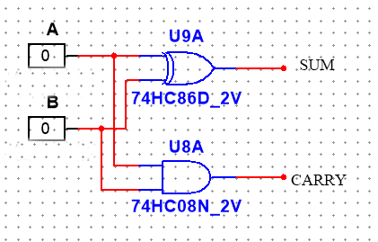
Figure 1: Half Adder
2.2. Full-Adder
The half-adder can be used for multi-bit addition operations. Some addition operations that do not contain the carry can be realized by connecting multiple half-adders in series. If it is needed to use the carry for addition operations, can use the full adder. The full adder can realize the addition operation of two one-bit binary numbers and one one-bit carry, and can be used for multi-bit include carry calculation. Table 2 shows the truth table of full adder.
Table 2: Truth table of full adder
A | B | C | SUM | C |
0 | 0 | 0 | 0 | 0 |
0 | 1 | 0 | 1 | 0 |
1 | 0 | 0 | 1 | 0 |
1 | 1 | 0 | 0 | 1 |
0 | 0 | 1 | 1 | 0 |
0 | 1 | 1 | 0 | 1 |
1 | 0 | 1 | 0 | 1 |
1 | 1 | 1 | 1 | 1 |
From the truth table, SUM can be seen as an XOR output when there is no carry input, and can be seen as an XOR non-output when there is carry input. The output result can be reversed by combining the carry with the XOR gate. When A and B are both 1, the carry of the output must be 1. When A and B are both 0, the carry of the output must be 0. When A and B are different, only when the input carry is 1 can the carry be output. Therefore, the carry output can be realized by using the combination with the gate or the structure of the gate. The structure of the full adder is show as Figure 2.
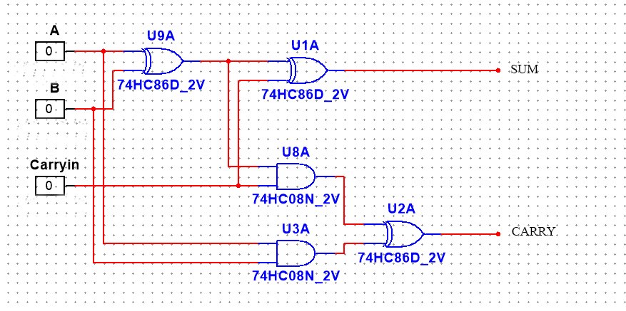
Figure 2: Full Adder
2.3. Comparator
The comparator is a circuit that can compare two values. When the input size is different, there are different output results. The truth table is shown in Table 3.
Table 3: Truth table of comparator
A | B | A>B | A=B | A<B |
0 | 0 | 0 | 1 | 0 |
0 | 1 | 0 | 0 | 1 |
1 | 0 | 1 | 0 | 0 |
1 | 1 | 0 | 1 | 0 |
Use the non-gate to make the output 0 when the two numbers are the same. When the two numbers are different, only when the large number does not pass the non-gate can the output be 1, and the output is divided. Therefore, it can be got the comparator circuit as shown in Figure 3.
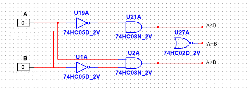
Figure 3: Comparator
3. Circuit Design
3.1. Absolute circuit with a half adder
To realize a four-bit absolute value circuit, the symbol bit of the four-bit binary number must be determined first. When the symbol bit is 0, the last three bits are retained as the amplitude. When the symbol bit is 1, it is needed to take its complement to compare. The complement code needs to add 1 after all the digits are reversed. Therefore, it is necessary to combine the adder to realize the inverse operation. First, it is necessary to determine whether the input symbol bit is 1. When the judgment is 1, each bit of data is inverted. When the judgment is 0, the original value is retained for comparison. Therefore, the XOR gate is first selected to invert each digit. When the symbol bit is 0, the output and input can be kept unchanged. When the symbol bit is 1, the output and input can be inverted.
When choosing adder, full adder and half adder can be chosen. The full adder can realize the calculation of the carry number, but the need for more gates will lead to more energy consumption and delay increase. And the complement code only needs to add one to the inverse code, and does not involve carry input. Assuming that the inverse code is A, it can be regarded as the sum of the input B and C of the full adder is never greater than 1, and no additional carry will be generated. Therefore, 1 and input carry 0, output carry and 0 can be merged into the next input directly using the half adder, which can significantly reduce the use of logic gates. The carry of the output is connected to one input of the next half adder, and the data to be calculated is connected to another input of the half adder. Finally, a logic circuit of the complement code can be obtained. This part of the circuit is shown in Figure 4.
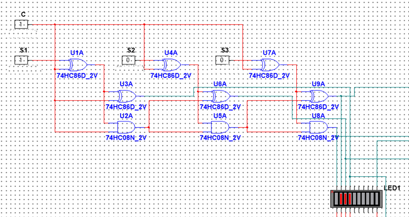
Figure 4: Absolute Circuit
As shown in Figure 4, when the input is 1001, it is 0110 after taking the reverse, and 0111 after adding 1. When the input is 1000, the output is 1000. In this case, circuit regard it as an amplitude of 8, which will be used for the subsequent absolute value comparison.
3.2. Three-bit comparator
The three-bit comparator can compare two three-bit binary numbers, and output 1 when the number of comparisons is greater than a value, otherwise the output bit is 0. Starting from the highest bit, when the input is the same as the threshold, it will be transferred to the next level for comparison. First, the NOT gate is combined with the AND gate, and finally a OR NOT gate is linked, which can achieve the output of 1 when the input is the same. If all the values are the same, the output is 0 directly. When the two numbers are not the same, the OR gate outputs 0, and then the situation is determined by whether the highest bit is higher than the threshold. If it is higher than the threshold, the output is 1, and the final output is 1 by combining the OR gate. If it is less than the threshold, the output is 0, the output of the AND gate is 0, and the OR gate input is 0 to achieve the final output of 0. When the two values are the same, the next comparison is entered, and the final result is obtained by comparing with the threshold, and then the same is true. The circuit is shown in Figure 5.
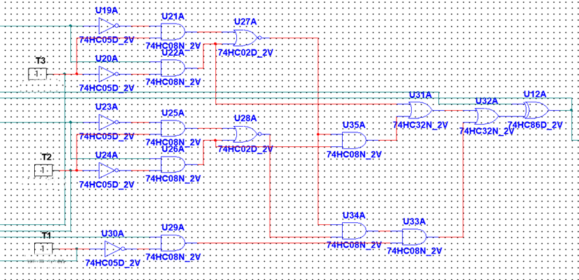
Figure 5: three-bit comparator
The comparator shown in Fig.5 can realize the comparison of three-digit data, and the comparison of the last three-digit data can be realized. If the input data is 1000, the comparison will only compare the threshold with the input 000, and eventually the opposite result will be obtained, so an XOR gate is used to reverse the result at the end. Finally, the comparison of absolute values can be achieved. When the input is greater than the threshold, the output of the circuit is 1. The total circuit diagram is shown in Figure 6. For example, when the input is 1110, its amplitude is 010, which is larger than the threshold voltage, so the output is 1.
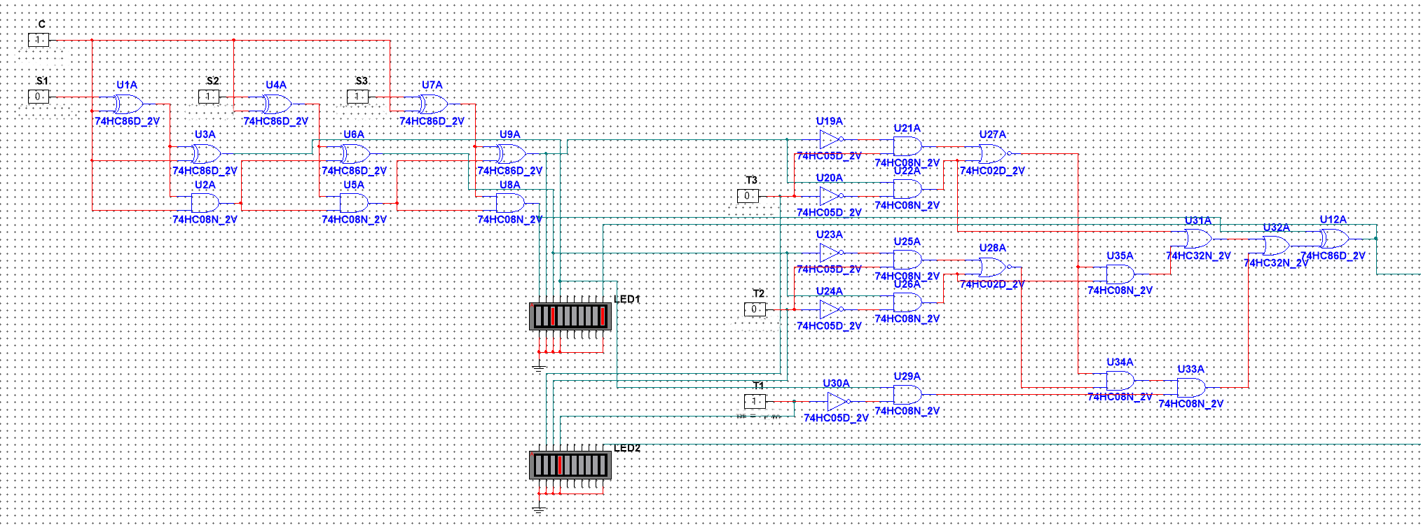
Figure 6: Total Circuit
4. Conclusion
The absolute value comparator is a circuit that can compare the input value with the threshold voltage. The four-bit binary absolute value comparator is composed of a four-bit absolute value circuit linked to a four-bit comparator, which can take the absolute value of the four-bit symbolic number and compare it with the threshold. First of all, it is a circuit that takes the absolute value. The absolute value can be taken by adding 1 to the reverse of the four-bit signed number, so it is necessary to use the four-bit adder to take the absolute value of the input number. In this paper, a half adder is selected to optimize the design of the circuit, which can reduce the delay and energy consumption of the system to a certain extent. The comparator can compare two values and output different results according to different situations. Connecting multiple comparators can achieve multi-digit comparison. By comparing the three-bit comparator with the output three-bit data, the function of comparing the absolute values of the four-bit signed numbers can be realized. When the output symbol bit is 1 but the amplitude is 000, the determined amplitude is 8 but not 0, so the circuit is specially designed when the symbol bit is 1 to ensure that the amplitude comparison will not be wrong.
This study provides a feasible solution for the design of four-digit signed absolute value comparators, which can use ready-made adders and comparators for rapid design and put into use. The absolute value comparator can be used where there are requirements for amplitude detection, and this absolute value comparator has room for extension. It can increase the number of bits detected by adding adders and comparators, and can be applied to more variable numerical detection environments.
However, there are still many shortcomings in this study. For example, the comparator part can still be optimized for other circuit structures, and the optimal state of delay and power consumption is not given. In the future, other schemes can be used to improve. Moreover, the system is built by a logic gate circuit, which can be used in practical applications using off-the-shelf adders and comparators. Therefore, alternative versions of off-the-shelf adders and comparators can be used in the future to reduce design costs and improve design efficiency.
References
[1]. Li Lin, Zhang Yuejun, Zhang Huihong. Full adder design based on line calculation [J]. Journal of Ningbo University (Sci-Tech Edition), 2022,35 (01) : 40-47.
[2]. Research on the application of Multisim11 in the teaching of ' Electrical Technology Foundation and Skills ' [D].Shanghai Normal University, 2013.
[3]. Zhao Junhong.Integrated high-performance low-power Quasi-Pseudo-NMOS / DT-CPL-TG full adder circuit design [D]. Xi 'an University of Electronic Science and Technology, 2007.
[4]. KUMNGERN M,KNOBNOB B,DEJHAN K.High frequency and high precision CMOS half-wave rectifier [J].Circuits,Systems and Signal Processing,2.
[5]. GIFT S J G,MAUNDY B.Versatile precision full-wave rectifiers for instrumentation and measurements [J].IEEE Transactions on Instrumentation and Measurements,2007,56(5):1703-1710.010,29(2010):815-836.
[6]. Li Weimin, Chu Yuxiao. Simulation analysis and application of numerical comparator circuit [J].Computer disc software and application, 2014,17 (14) : 289 + 291.
[7]. Han Dawei. Application and Exploration of NI Multisim Software in Digital Circuit Virtual Simulation Teaching [J].Communication World, 2024,31 (08) : 61-63.
[8]. The application of Multisim in the teaching of ' Electrical Technology ' [J].Electronics, 2011,24 (02) : 124-126.
[9]. Liu Jie, Yi Maoxiang. Research on 4-adder parallel adder and extended interface [J].Journal of Hefei University of Technology (Natural Science Edition), 2009,32 (11) : 1683-1686.
[10]. Yi Yingping, Hou Wen, Jiang Ling, et al. 2-digit numerical comparator design method discussion [J]. Education and Teaching Forum, 2016, (37) : 185-186.
Cite this article
Dai,H. (2025). 4-bit Absolute-Value Detector Based on Multisim. Applied and Computational Engineering,128,7-12.
Data availability
The datasets used and/or analyzed during the current study will be available from the authors upon reasonable request.
Disclaimer/Publisher's Note
The statements, opinions and data contained in all publications are solely those of the individual author(s) and contributor(s) and not of EWA Publishing and/or the editor(s). EWA Publishing and/or the editor(s) disclaim responsibility for any injury to people or property resulting from any ideas, methods, instructions or products referred to in the content.
About volume
Volume title: Proceedings of the 5th International Conference on Materials Chemistry and Environmental Engineering
© 2024 by the author(s). Licensee EWA Publishing, Oxford, UK. This article is an open access article distributed under the terms and
conditions of the Creative Commons Attribution (CC BY) license. Authors who
publish this series agree to the following terms:
1. Authors retain copyright and grant the series right of first publication with the work simultaneously licensed under a Creative Commons
Attribution License that allows others to share the work with an acknowledgment of the work's authorship and initial publication in this
series.
2. Authors are able to enter into separate, additional contractual arrangements for the non-exclusive distribution of the series's published
version of the work (e.g., post it to an institutional repository or publish it in a book), with an acknowledgment of its initial
publication in this series.
3. Authors are permitted and encouraged to post their work online (e.g., in institutional repositories or on their website) prior to and
during the submission process, as it can lead to productive exchanges, as well as earlier and greater citation of published work (See
Open access policy for details).
References
[1]. Li Lin, Zhang Yuejun, Zhang Huihong. Full adder design based on line calculation [J]. Journal of Ningbo University (Sci-Tech Edition), 2022,35 (01) : 40-47.
[2]. Research on the application of Multisim11 in the teaching of ' Electrical Technology Foundation and Skills ' [D].Shanghai Normal University, 2013.
[3]. Zhao Junhong.Integrated high-performance low-power Quasi-Pseudo-NMOS / DT-CPL-TG full adder circuit design [D]. Xi 'an University of Electronic Science and Technology, 2007.
[4]. KUMNGERN M,KNOBNOB B,DEJHAN K.High frequency and high precision CMOS half-wave rectifier [J].Circuits,Systems and Signal Processing,2.
[5]. GIFT S J G,MAUNDY B.Versatile precision full-wave rectifiers for instrumentation and measurements [J].IEEE Transactions on Instrumentation and Measurements,2007,56(5):1703-1710.010,29(2010):815-836.
[6]. Li Weimin, Chu Yuxiao. Simulation analysis and application of numerical comparator circuit [J].Computer disc software and application, 2014,17 (14) : 289 + 291.
[7]. Han Dawei. Application and Exploration of NI Multisim Software in Digital Circuit Virtual Simulation Teaching [J].Communication World, 2024,31 (08) : 61-63.
[8]. The application of Multisim in the teaching of ' Electrical Technology ' [J].Electronics, 2011,24 (02) : 124-126.
[9]. Liu Jie, Yi Maoxiang. Research on 4-adder parallel adder and extended interface [J].Journal of Hefei University of Technology (Natural Science Edition), 2009,32 (11) : 1683-1686.
[10]. Yi Yingping, Hou Wen, Jiang Ling, et al. 2-digit numerical comparator design method discussion [J]. Education and Teaching Forum, 2016, (37) : 185-186.