


1. Introduction
Since the signing of the Paris Agreement in 2016, increasing the share of clean energy in power generation has become a major global development trend in power systems. Numerous nations have shown interest in photovoltaic (PV) grid-connected power generating technology since solar energy is one of the most dependable renewable energy sources and has substantial expansion potential. When solar panels are exposed to sunlight, the DC they produce cannot be directly linked to the AC transmission system; instead, an inverter is required to convert the DC to AC. Based on their topologies, PV grid-connected inverters can be categorized as isolated and non-isolated categories. Compared to isolated inverters, non-isolated inverters are smaller in size, lower in cost, and have a simpler structure. One of their most notable advantages is the ability to enhance system efficiency, making them particularly attractive for PV power generation systems, which often face high generation costs [1]-[4]. Therefore, studying and optimizing non-isolated inverters is of great practical importance in reducing power generation costs and improving energy utilization.
However, due to the absence of isolation in non-isolated inverters, various filter inductors and capacitors on the DC side, along with parasitic capacitances and the AC grid-connected inverter circuit, are interconnected. These parts work together to create a resonant network that eventually causes a sizable leakage current that reaches ground via the grounding loop. [5]. Leakage current can severely impact the power generation system by increasing harmonic current, degrading power grid quality, increasing system losses, and creating safety and electromagnetic compatibility issues [6]. To gain widespread development and application in power production systems, non-isolated PV inverters must overcome the crucial technological issue of suppressing or avoiding leakage current.
Currently, many domestic and international experts and researchers have proposed solutions to suppress or eliminate leakage current. In general, these solutions fall into one of two primary categories: modifying the circuit structure and innovating the modulation strategy [7]. This paper focuses exclusively on methods related to modifying the circuit structure, and the reasons for this will be discussed in the main text. Compared to single-phase inverters, three-phase inverters significantly improve reliability and extend service life, making them widely used in PV power generation systems. Existing solutions are divided into two main approaches: implanted capacitors and modified topologies. This paper compares the advantages and application scopes of these methods. Finally, future development directions and challenges for leakage current suppression technology are discussed, providing valuable reference points for further optimization of leakage current suppression techniques.
2. Principle model of leakage current in photovoltaic inverter
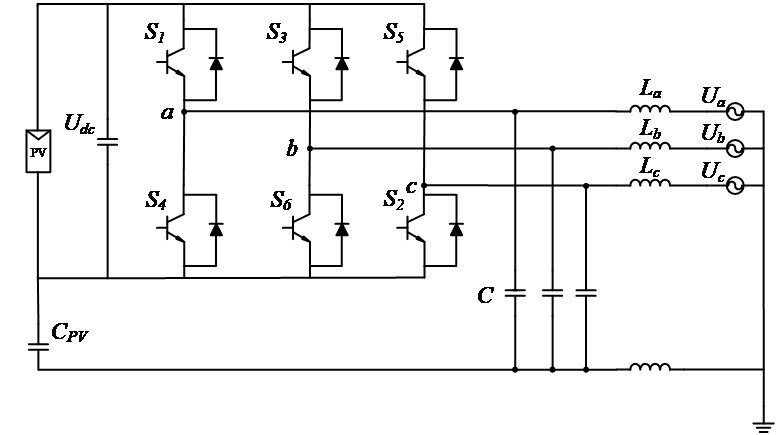
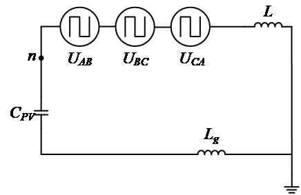
Before studying leakage current suppression technologies, it is crucial to first understand the principle of leakage current generation and identify its root causes to develop effective solutions. Figure 1 presents a schematic circuit diagram of a traditional three-phase non-isolated photovoltaic inverter. In the diagram, La, Lb, and Lc are the inductors at the grid connection points, and C represents the parasitic capacitance between the output of the three-phase bridge inverter circuit and the ground. The parasitic capacitance between the solar panel and the ground is denoted by Cpy, whereas the ground inductance between the inverter and the grid is represented by Lg. Based on figure 1, the equivalent common-mode voltage model of the system is established in figure 2, where Ua, Ub, and Uc represent the branch voltages of the three phases. From this model, the common-mode voltage and differential-mode voltage between any two phases can be derived:
\( {U_{cmij}}-\frac{{U_{in}}+{U_{jn}}}{2}\ \ \ (1) \)
\( {U_{dmij}}-\frac{({U_{in}}-{U_{jn}})({L_{i}}-{L_{j}})}{2({L_{i}}+{L_{j}})}\ \ \ (2) \)
By using the formula above, one may get the system's total mode voltage:
\( {U_{tcm}}-\frac{{U_{cmAB}}+{U_{cmBC}}+{U_{cmCA}}}{3}+\frac{{U_{dmAB}}+{U_{dmBC}}+{U_{dmCA}}}{3}\ \ \ (3) \)
If the inductors La、Lb and Lc at the grid-connected place can be set to be equal respectively, the simplified total mode voltage can be obtained [8]:
\( {U_{tcm}}-\frac{{U_{An}}+{U_{Bn}}+{U_{Cn}}}{3}\ \ \ (4) \)
Furthermore, the common-mode voltage Ucm and the voltage Uon at each tip of the parasitic capacitor have the following transfer functions:
\( {U_{on}}(s)=G(S){U_{cm}}(s)\ \ \ (5) \)
\( G(s)=\frac{1}{1+\frac{2LCpν}{3}{s^{2}}}\ \ \ (6) \)
|
| |
Figure 1: Three-phase non-isolated PV inverter. | Figure 2: System common-mode voltage equivalence model. |
The relationship between the common mode leakage current ileakage and the voltage Uon at both ends of the parasitic capacitor is as follows:
\( {i_{leakage}}=C\frac{d{U_{on}}}{dt}\ \ \ (7) \)
The common-mode voltage, differential-mode voltage, parasitic capacitance to ground, and circuit parasitic characteristics are among the components that ultimately affect the leakage current. Therefore, the effective control and optimization of these circuit parameters are crucial to the success of leakage current suppression technologies.
3. Leakage current suppression technology by modifying circuit structure
According to the analysis of leakage current generation above, the inverter circuit is common-mode loop impedance, parasitic capacitance to ground, and common-mode voltage all affect leakage current generation. Therefore, after reviewing relevant literature, several effective solutions have been identified. Among these, two mainstream approaches stand out:
Modifying the circuit structure: This includes altering the positions of components within the circuit or adding/removing components as necessary.
Proposing or improving modulation strategies: Modulation strategies refer to control methods that manage the operation of all switches in the circuit according to a specific logical sequence. However, new control strategies are generally introduced to complement new circuit topologies.
Since new modulation strategies are often designed for specific new topologies, this paper focuses on the more fundamental approach of modifying the circuit structure. In the following sections, the author categorizes these methods into two primary technical research directions: implanting appropriate capacitors and modifying the circuit topology.
3.1. Implanting appropriate capacitors
3.1.1. Adding Bypass Capacitors on the DC Side
It was suggested to use a new grid-connected solar inverter based on the DC [9] bypass topology. It is well known that the common-mode loop impedance and the common-mode voltage are correlated with the common-mode leakage current in a system. Therefore, methods for reducing leakage current can be considered from two perspectives: (1) limiting the variation range of the common-mode voltage and (2) increasing the impedance of the common-mode loop.
Figure 3: New H7 DC bypass topology.
Figure 5: Three-phase three-level inverter with neutral point capacitor. |
Figure 4: A combined inverter with flying capacitors. |
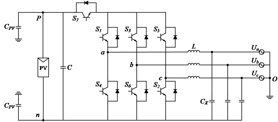
To further reduce the common-mode leakage current in the H7 DC bypass topology, this method increases the impedance of the common-mode loop. To achieve this, a bypass capacitor Cx is added after the three-phase filter inductor, with the common terminal of Cx connected to the negative terminal of the DC side, as shown in figure 3. Under this structure, the formula for the leakage current is:
\( {i_{leakage}}(s)={G_{c2}}(s){U_{cm}}(s)\ \ \ (8) \)
Gc2(s) becomes smaller under this topology, resulting in smaller leakage currents. Therefore, the improved topology has a better effect on the suppression of leakage current, and the larger the bypass capacitance, the better the effect.
3.1.2. Adding Flying Capacitors
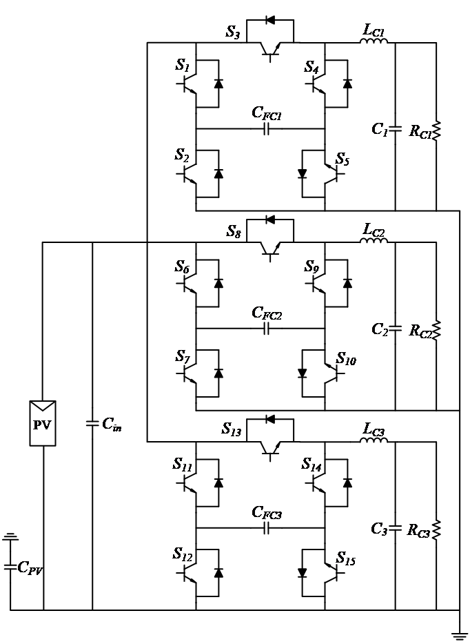
A combined inverter with flying capacitors [10] was proposed. The circuit design of a combined three-phase PV inverter with flying capacitors is shown in figure 4. In this design, CFC1, CFC2 and CFC3 are flying capacitors, and the topology divides the system into three independently decoupled single-phase circuits, with each phase operating independently of the others.
For a combined three-phase inverter, the total leakage current is the sum of the leakage currents of each phase. To achieve zero total leakage current, the overall common-mode voltage must remain constant. The flying capacitors are charged by the photovoltaic cells during the positive half-cycle and discharge during the negative half-cycle, maintaining the common-mode voltage of each phase. This ensures that the total common-mode voltage of the system remains constant, effectively eliminating the leakage current. However, this circuit is more complex than traditional three-phase circuits. It requires additional switches, resulting in higher costs and increased total switching losses.
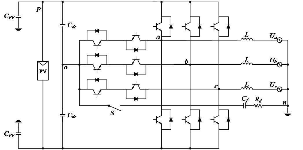
3.1.3. Adding Neutral Point Capacitors
|
| |
(a) | (b) |
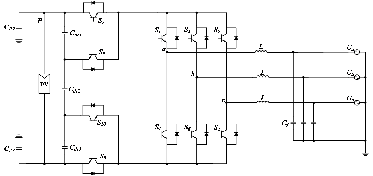
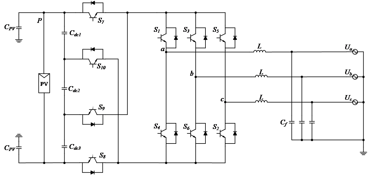
Figure 6: Forward and reverse clamp H10 three-phase inverter topology.
A three-phase inverter with a neutral point capacitor [11] is proposed. The grid-connected structure of the improved non-isolated three-phase, three-level inverter is shown in figure 5. In this design, the neutral point on the AC side and the neutral point on the DC side are connected by a capacitor Cf, forming a common-mode LC filter circuit for leakage current suppression. This filter circuit effectively filters out the high-frequency components of the common-mode voltage without affecting the differential-mode loop. This circuit topology has a significant effect on suppressing leakage current and has minimal impact on the differential-mode grid-connected current. Moreover, it does not require changes to the modulation strategy or control method of the grid-connected system, making the principle straightforward and easy to implement, with substantial engineering application potential. However, the numerical settings of the filter parameters depend on the specific parameters and structure of the circuit to which the method is applied. This means that when applied to different inverter circuits, a series of experiments must be conducted to determine the optimal values for Cf and Rd. This requirement poses challenges for the widespread application of this method.
There are other similar methods that involve adding appropriate capacitors to the inverter circuit, including the method described in this paper. These approaches are generally simple to implement and do not significantly alter the circuit structure. Furthermore, they typically do not introduce a large number of additional electronic components, thus not significantly increasing the overall cost. However, the lifespan of the capacitors can affect their performance and, in turn, impact the stability and service life of the entire inverter circuit.
3.2. Changing the circuit topology
3.2.1. Adding clamping circuitry
Ref. [12] proposes a 10-switch three-phase inverter topology (H10 topology) with two different clamping modes: forward and reverse. The forward clamped H10 three-phase inverter topologies and their corresponding schematic designs are displayed in figures 6(a) and 6(b), respectively.
In this design, two DC bus disconnectors and a clamping circuit are added to the traditional three-phase inverter topology. The location of the clamping switches within the clamping circuit is the primary distinction between the two topologies. Inverter system common-mode performance is enhanced by both topologies, which also lessen the common-mode voltage's variable range and successfully address the issue of system leakage current. When compared to forward topology, the reverse topology exhibits a higher common-mode voltage frequency, larger common-mode loop impedance, and stronger leakage current suppression, making it more advantageous for engineering applications.
However, regardless of the type of clamping circuit used, both structures are relatively complex. Four additional switch devices are introduced on top of the original three-phase bridge, which significantly increases both the cost and the overall switching losses of the circuit.
3.2.2. Replacing the boost converter with a buck-boost converter and connecting it to a three-phase bridge arm
The methods introduced above focus primarily on modifications of voltage-source inverters (VSIs). In this section, we will introduce a more specialized type of current-source inverter (CSI). A current-source inverter is distinguished by the fact that the DC side functions as a current source, with the DC power supply being roughly represented as a continuous current source thanks to the use of massive inductors for filtering.
In the conventional three-phase current-source inverter (CSI), a boost converter is multiplexed with the three-phase bridge arm, giving the CSI a boost characteristic. Theoretically, based on this design approach, an inverter with buck-boost capability can be realized by connecting a buck-boost converter to the three-phase bridge arm. The structure proposed in Ref. [13] is shown in figure 7.
Compared to the traditional CSI, this design connects two energy storage inductors in series on the DC side and adds three more switching transistors S7~ S9, as well as two diodes D8 and D9, on the DC side. The midpoint of the DC side is directly connected to the filter capacitor center of the AC side. This design provides a broad range of application situations and enables both step-up and step-down voltage conversion of the input voltage, satisfying the needs of various voltage levels. Furthermore, this circuit design stabilizes the common-mode voltage under sinusoidal pulse width modulation (SPWM), and the modulation technique is straightforward and simple to use. The leakage current generated by this topology also meets the VDE0126-1-1 standard under grid-connected conditions.
However, compared to traditional three-phase voltage-source inverters, this design requires eight additional diodes, three switching transistors, and two inductors, significantly increasing the circuit's cost, especially due to the large inductors used for current stabilization. Additionally, the output voltage of this method varies with the load, making it less stable than that of a voltage-source inverter circuit.
Both of the methods described above, which involve changes to the circuit topology, introduce varying degrees of complexity to the circuit structure. This complexity is also present in multi-level inverters, where more levels mean more switches, resulting in higher costs, larger volumes, more complex circuitry, and more intricate modulation strategies. Although these designs provide better leakage current suppression and special features, they also come with higher costs and increased switching losses.
4. Discussion
The above leakage current suppression schemes are summarized and compared based on their characteristics, shortcomings, leakage current suppression capabilities, and application range, as shown in table 1.
If we focus solely on leakage current suppression, the method of using flying capacitors achieves the best results. It completely eliminates leakage current under symmetrical loads and almost fully suppresses it under asymmetrical loads [10], while other methods show relatively lower effectiveness.
Table 1: Comparison of leakage current suppression methods
Method category | Leakage current suppression method | peculiarity | Leakage current suppression capability | shortcoming | Scope of application |
Implant the appropriate capacitors | Access bypass capacitors on the DC side | Increase the common-mode impedance of the common-mode loop | Good | The stability of the system is affected by the lifetime of the implanted capacitor | The larger the bypass capacitance, the better; At present, it has been verified in low-power scenarios |
Access fly-across capacitors | The flying capacitor is charged in the positive half cycle and discharged in the negative half cycle of operation | Great (almost completely suppressed) | The circuit is more complex, and the cost is higher than that of traditional three-phase circuits | It is easy to realize three-phase decoupling control, and has strong asymmetric load capacity | |
Access to neutral point capacitors | The neutral point on the AC side and the neutral point on the DC side are connected by capacitors | Good | Filter parameters need to be redesigned for different topologies | The high-frequency component of the common-mode voltage is effectively filtered out, and has little influence on the differential mode grid-connected current. It is easy to implement and has a wide range of applicability | |
Change the circuit topology | Clamping circuitry is added | Add two DC bus disconnectors and a clamping circuit | Good | The structure becomes more complex, increasing the cost and total loss | It can improve the common-mode characteristics and effectively suppress the leakage current; Meets VDE0126-1-1 standard |
Use the Buck-Boost structure | A buck-boost converter is used in combination with an inverter circuit | Good | The structure becomes more complex, increasing the cost and total loss | The modulation is simple and can realize the function of buck-boosting pressure; It can meet the requirements of different voltage levels and meet the VDE0126-1-1 standard |
The methods described in this paper represent several different approaches to leakage current suppression. The method of adding a bypass capacitor on the DC side increases the common-mode impedance of the loop through the capacitor. The idea behind using flying capacitors is to incorporate them into the control process, allowing them to charge during the positive half-cycle and discharge during the negative half-cycle of operation. The method of adding a neutral point capacitor filters out the high-frequency components of the common-mode voltage by connecting the neutral points on the AC and DC sides with a capacitor and resistor to create a filter circuit. The clamping circuit approach uses a clamping circuit to reduce the common-mode voltage's fluctuation range. Lastly, the current-source inverter method differs from previous voltage-source inverter circuits and provides an alternative approach.
As summarized in table 1, each method has its own advantages, disadvantages, and optimal application scenarios. First, several methods involving implanted capacitors are analyzed. In the method of increasing the common-mode impedance of the common-mode loop, the larger the key capacitor used, the better the suppression effect. While using flying capacitors increases circuit complexity, it enables easier three-phase decoupling control and provides strong support for asymmetric loads. Although multiple experiments are required to determine the optimal filtering parameters for different inverter circuits, this approach effectively filters leakage current with minimal impact on differential-mode voltage. Overall, most capacitor implantation methods require only minor modifications to the original inverter circuit, making them relatively simple to implement. They involve a few additional electronic components, resulting in minimal cost increases. However, capacitor lifespan is a key consideration, as their performance degrades over time, potentially affecting the overall functionality and stability of the circuit.
Next, the methods involving changes to the circuit topology are analyzed. The addition of a clamping circuit improves the common-mode characteristics, effectively suppressing leakage current. Meanwhile, the current-source inverter with a buck-boost structure provides voltage step-up and step-down functions to meet different voltage level requirements, but the output voltage of current-source inverters tends to be unstable and varies with load, which is a significant drawback. In general, changing the circuit topology results in good leakage current suppression, and some methods may offer additional practical functionalities. However, most of these methods introduce more electronic components, such as switches, which can significantly increase both the cost and the overall electronic losses.
5. Conclusion
This research examines two methods for decreasing leakage current by changing the circuit structure, as well as the principle model of leakage current generation. The respective advantages, disadvantages, and scopes of application are analyzed, leading to the following conclusions:
1. The method of suppressing leakage current by implanting appropriate capacitors in the inverter circuit is generally simple and easy to implement. However, the impact of capacitor lifespan on system stability cannot be ignored.
2. Strategies that drastically change the circuit topology typically introduce more electrical components, which increases both the cost and power loss of the inverter. Nonetheless, these approaches offer better leakage current suppression and may provide additional advantages and functionalities, making them feasible for practical applications.
Based on these findings, the author also has some thoughts regarding future research directions for leakage current suppression technology:
1. In the research field focused on implanting capacitors to achieve leakage current suppression, optimizing the function and lifespan of the target capacitors could be considered. This would reduce system maintenance costs, extend service life, and improve system stability.
2. New modulation strategies could be developed for novel inverter circuit topologies. By reducing the number of switches without compromising leakage current suppression, circuit losses could be minimized. The optimal modulation strategy should be selected based on different application environments to balance performance and efficiency.
References
[1]. Singh, G. K. (2013). Solar power generation by PV (photovoltaic) technology: A review. Energy, 53, 1-13.
[2]. Wang, J., Mu, X., & Li, Q.-K. (2017). Study of passivity-based decoupling control of T-NPC PV grid-connected inverter. IEEE Transactions on Industrial Electronics, 64(9), 7542-7551.
[3]. Zhou, L., Gao, F., Wang, W., & Preindl, M. (2018). Transformerless three phase NPC inverter with reduced switches. In 2018 IEEE Energy Conversion Congress and Exposition (ECCE) (pp. 4766-4770). Portland, OR, USA.
[4]. Xuan, Y., Tian, M., Song, X., Chen, W., & Yang, X. (2015). Design and implementation of a high power three-level T-type inverter for a photovoltaic system. In 2015 9th International Conference on Power Electronics and ECCE Asia (ICPE-ECCE Asia) (pp. 2808-2813). Seoul, Korea (South).
[5]. Dadkhah, J., Ho, C. N. M., & Siu, K. K.-M. (2024). Three-Phase Transformerless PV Inverter With Reconfigurable LCL Filter and Reactive Power Capability. IEEE Transactions on Power Electronics, 39(7), 8229–8241.
[6]. Upadhiya, A. K., Lakshminarasamma, N., & Mishra, M. K. (2024). An eleven-level self-balancing switched-capacitor based inverter with five-fold voltage gain. IEEE Transactions on Industry Applications, 60(5), 7138–7155.
[7]. Guo, X., et al. (2018). Leakage current suppression of three-phase flying capacitor PV inverter with new carrier modulation and logic function. IEEE Transactions on Power Electronics, 33(3), 2127-2135.
[8]. Guo, X., Yang, Y., & Zhu, T. (2018). ESI: A Novel Three-Phase Inverter With Leakage Current Attenuation for Transformerless PV Systems. IEEE Transactions on Industrial Electronics, 65(4), 2967–2974.
[9]. He, S., Wang, F., Wang, Y., & Liu, B. (2023). Modeling and suppression of zero-sequence circulating current resonance for parallel interleaved inverters with bypass capacitor-based leakage current mitigation. IEEE Journal of Emerging and Selected Topics in Power Electronics, 11(3), 3097-3107.
[10]. Liu, C., et al. (2022). Leakage current suppression of transformerless 5L-ANPC inverter with lower ripple model predictive control. IEEE Transactions on Industry Applications, 58(5), 6297–6309.
[11]. Zhang, C., Jiang, Y., Xing, X., Li, X., Qin, C., & Zhang, B. (2023). Passivity-based control method for three-level photovoltaic inverter to mitigate common-mode resonant current. IEEE Transactions on Industrial Informatics, 19(9), 9733-9744.
[12]. But, H. X., Shao, P. C., & Lan, Z. X. (2021). Comparative analysis of leakage current suppression capability of forward-clamped and reverse-clamped H10 three-phase inverters. IET Power Electronics, 14(16), 2563–2573.
[13]. Yao, Z., & He, X. (2024). Three-phase common-ground-type photovoltaic inverter without shoot-through problem. Int J Circ Theor Appl, 52(10), 5252–5262.
Cite this article
Wang,C. (2025). Advanced Leakage Current Suppression Techniques for Three-Phase Non-Isolated Photovoltaic Inverters: A Focus on Structural Modifications. Applied and Computational Engineering,127,90-98.
Data availability
The datasets used and/or analyzed during the current study will be available from the authors upon reasonable request.
Disclaimer/Publisher's Note
The statements, opinions and data contained in all publications are solely those of the individual author(s) and contributor(s) and not of EWA Publishing and/or the editor(s). EWA Publishing and/or the editor(s) disclaim responsibility for any injury to people or property resulting from any ideas, methods, instructions or products referred to in the content.
About volume
Volume title: Proceedings of the 5th International Conference on Materials Chemistry and Environmental Engineering
© 2024 by the author(s). Licensee EWA Publishing, Oxford, UK. This article is an open access article distributed under the terms and
conditions of the Creative Commons Attribution (CC BY) license. Authors who
publish this series agree to the following terms:
1. Authors retain copyright and grant the series right of first publication with the work simultaneously licensed under a Creative Commons
Attribution License that allows others to share the work with an acknowledgment of the work's authorship and initial publication in this
series.
2. Authors are able to enter into separate, additional contractual arrangements for the non-exclusive distribution of the series's published
version of the work (e.g., post it to an institutional repository or publish it in a book), with an acknowledgment of its initial
publication in this series.
3. Authors are permitted and encouraged to post their work online (e.g., in institutional repositories or on their website) prior to and
during the submission process, as it can lead to productive exchanges, as well as earlier and greater citation of published work (See
Open access policy for details).
References
[1]. Singh, G. K. (2013). Solar power generation by PV (photovoltaic) technology: A review. Energy, 53, 1-13.
[2]. Wang, J., Mu, X., & Li, Q.-K. (2017). Study of passivity-based decoupling control of T-NPC PV grid-connected inverter. IEEE Transactions on Industrial Electronics, 64(9), 7542-7551.
[3]. Zhou, L., Gao, F., Wang, W., & Preindl, M. (2018). Transformerless three phase NPC inverter with reduced switches. In 2018 IEEE Energy Conversion Congress and Exposition (ECCE) (pp. 4766-4770). Portland, OR, USA.
[4]. Xuan, Y., Tian, M., Song, X., Chen, W., & Yang, X. (2015). Design and implementation of a high power three-level T-type inverter for a photovoltaic system. In 2015 9th International Conference on Power Electronics and ECCE Asia (ICPE-ECCE Asia) (pp. 2808-2813). Seoul, Korea (South).
[5]. Dadkhah, J., Ho, C. N. M., & Siu, K. K.-M. (2024). Three-Phase Transformerless PV Inverter With Reconfigurable LCL Filter and Reactive Power Capability. IEEE Transactions on Power Electronics, 39(7), 8229–8241.
[6]. Upadhiya, A. K., Lakshminarasamma, N., & Mishra, M. K. (2024). An eleven-level self-balancing switched-capacitor based inverter with five-fold voltage gain. IEEE Transactions on Industry Applications, 60(5), 7138–7155.
[7]. Guo, X., et al. (2018). Leakage current suppression of three-phase flying capacitor PV inverter with new carrier modulation and logic function. IEEE Transactions on Power Electronics, 33(3), 2127-2135.
[8]. Guo, X., Yang, Y., & Zhu, T. (2018). ESI: A Novel Three-Phase Inverter With Leakage Current Attenuation for Transformerless PV Systems. IEEE Transactions on Industrial Electronics, 65(4), 2967–2974.
[9]. He, S., Wang, F., Wang, Y., & Liu, B. (2023). Modeling and suppression of zero-sequence circulating current resonance for parallel interleaved inverters with bypass capacitor-based leakage current mitigation. IEEE Journal of Emerging and Selected Topics in Power Electronics, 11(3), 3097-3107.
[10]. Liu, C., et al. (2022). Leakage current suppression of transformerless 5L-ANPC inverter with lower ripple model predictive control. IEEE Transactions on Industry Applications, 58(5), 6297–6309.
[11]. Zhang, C., Jiang, Y., Xing, X., Li, X., Qin, C., & Zhang, B. (2023). Passivity-based control method for three-level photovoltaic inverter to mitigate common-mode resonant current. IEEE Transactions on Industrial Informatics, 19(9), 9733-9744.
[12]. But, H. X., Shao, P. C., & Lan, Z. X. (2021). Comparative analysis of leakage current suppression capability of forward-clamped and reverse-clamped H10 three-phase inverters. IET Power Electronics, 14(16), 2563–2573.
[13]. Yao, Z., & He, X. (2024). Three-phase common-ground-type photovoltaic inverter without shoot-through problem. Int J Circ Theor Appl, 52(10), 5252–5262.