


1. Introduction
The structure of the paper is organized as follows: Chapter 1 presents the introduction, outlining the research background and significance; Chapter 2 details the design process, including the construction of the truth table and optimization of logic expressions; Chapter 3 provides an analysis of delay and power consumption, examining the effects of supply voltage and gate capacitance; finally, the conclusion summarizes the findings of the study.
With the rapid advancement of integrated circuit technology, 4-bit absolute value detectors have found widespread application in signal processing and digital circuit design. These detectors effectively enhance the processing efficiency and reliability of systems[1]. This paper aims to explore methods for improving circuit performance while minimizing delay and power consumption in the design and optimization of a 4-bit absolute value detector, addressing increasingly stringent energy consumption constraints. The study encompasses the design process of the 4-bit absolute value detector, an analysis of delay and power consumption, and the implementation of optimization strategies.
2. Design Process
The initial parameters for the detector are as follows: the minimum energy for a delay that is 50% longer than the minimum delay, the parasitic capacitance is equal to the gate capacitance, CL = 32, VDD = 1 V, and 0 < VDDopt < 1 V.
The primary objective of designing a 4-bit absolute value detector is to compute the absolute value of the input signal. First, the functional requirements of the detector are clarified, which include accepting a 4-bit binary number as input, comparing its corresponding absolute value with a given reference value, and outputting the comparison result. To achieve this goal, the design process is divided into several modules, including the construction of a truth table, simplification of logic expressions, implementation of logic gates, optimization of circuit delay, and identification of the minimum power consumption of the circuit.
2.1. Construct the truth table
Before designing the 4-bit absolute value detector, it is essential to clarify its functionality and operational principles. By analyzing the various combinations of input signals, a corresponding truth table is constructed. The truth table lists all possible input states along with their corresponding output results, ensuring that the design can accurately compute the absolute value. The input signal range is represented as the two's complement of a 4-bit binary number, corresponding to decimal values from -8 to 7.
2.2. Simplify logic expression
Based on the truth table, Karnaugh maps are employed to simplify the logic expressions. The Karnaugh map is a graphical method that effectively reduces the number of terms in the logic expressions [2]. The Karnaugh maps corresponding to S2, S1, and S0 are illustrated in Table 1, Table 2 and Table 3.
Table 1: K-map of S2 | ||||
a1a0\a3a2 | 00 | 01 | 11 | 10 |
00 | 0 | 1 | 1 | |
01 | 0 | 1 | 0 | 1 |
11 | 0 | 1 | 0 | 1 |
10 | 0 | 1 | 0 | 1 |
Table 2: K-map of S1 | ||||
a1a0\a3a2 | 00 | 01 | 11 | 10 |
00 | 0 | 0 | 0 | |
01 | 0 | 0 | 1 | 1 |
11 | 1 | 1 | 0 | 0 |
10 | 1 | 1 | 1 | 1 |
Table 3: K-map of S0 | ||||
a1a0\a3a2 | 00 | 01 | 11 | 10 |
00 | 0 | 0 | 0 | |
01 | 1 | 1 | 1 | 1 |
11 | 1 | 1 | 1 | 1 |
10 | 0 | 0 | 0 | 0 |
The results indicate that the design can be implemented with fewer logic gates, thereby reducing the complexity and power consumption of the circuit. By mapping the truth table, the simplified expressions are as follows:
\( S0=A0 \) (1)
\( S1=A3 \prime A1+A1A0 \prime +A3A1 \prime A0 \) (2)
\( S2=A3 \prime A2+A3A2 \prime +A2A1 \prime A0 \prime \) (3)
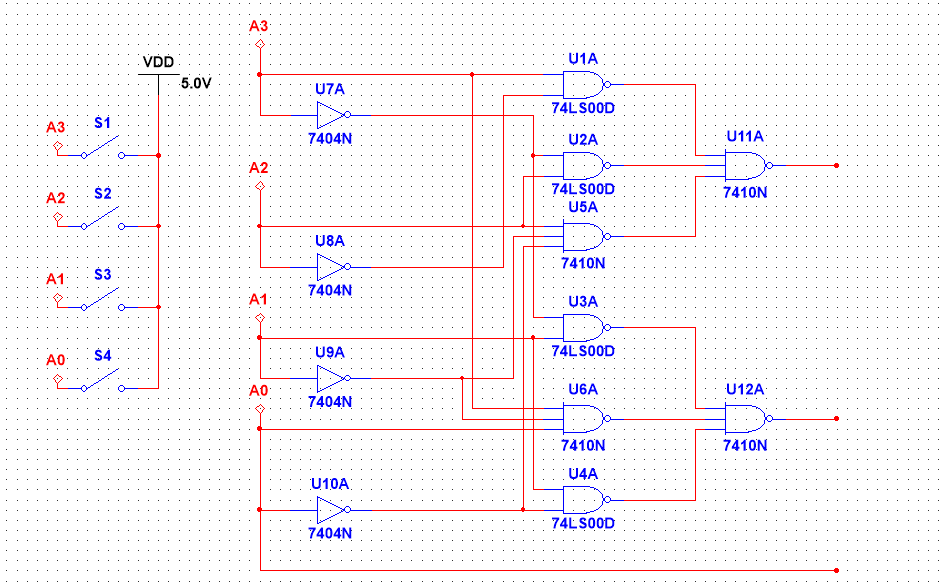
The above expressions will be used for the subsequent circuit implementation, allowing the drawing of the circuit. Figure 1 illustrates the realized circuit structure of the caculater, detailing the connections between various logic gates and their respective functions[3].
|
Figure 1: The circuit topology of the caculater |
2.3. Logic Gate Implementation
In selecting the logic gates, a combination of NAND gates, NOR gates, and inverters was used due to their advantages in delay computation [4]. In this design, all logical functions can be implemented using these gates, eliminating the need for other types of gates and resulting in a more streamlined and analyzable circuit structure [5].
The following section demonstrates how to simplify the logic expressions for the comparator:
\( F=A3B3 \prime +(A3B3+A3 \prime B3 \prime )A2B2 \prime +(A2B2+A2 \prime B2 \prime )(A3B3+A3 \prime B3 \prime )A1B1 \prime \) (4)
\( A3B3+A3 \prime B3 \prime =\bar{A3 \prime B3+A3B3 \prime } \) (5)
\( A2B2+A2 \prime B2 \prime =\bar{A2 \prime B2+A2B2 \prime } \) (6)
2.4. Circuit Optimization
After implementing the preliminary design, circuit optimization was performed to reduce delay and power consumption. By analyzing the critical paths of the circuit, the parts with the most significant delay were identified and specifically optimized to achieve lower delay and power consumption while maintaining circuit functionality.
2.5. Design Verification
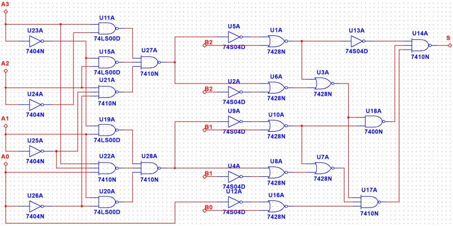
Upon completion of the design, simulation software was used to verify the circuit. Various input conditions were set to observe whether the circuit outputs met the expected results. During the verification process, delay and power consumption under different input conditions were recorded to ensure that the circuit could operate stably in practical applications and meet design requirements[6]. Figure 2 illustrates the overall circuit structure, demonstrating that this logic circuit effectively fulfills its intended function.
|
Figure 2: The total design of the circuit topology |
3. Delay and Power Consumption Analysis
In the design of circuits, delay and power consumption are two critical performance metrics that directly impact the overall performance and functionality of the circuit. Delay determines the time taken for a signal to propagate from input to output, excessive delay can reduce the circuit's response speed and adversely affect the system's real-time performance. Power consumption relates to the energy efficiency of the circuit. A low-power design not only extends the battery life of devices but also minimizes heat generation, thereby enhancing system stability [7]. Therefore, a comprehensive analysis of both delay and power consumption during the early stages of circuit design is essential to establish effective optimization strategies, ensuring the final product meets both performance and efficiency requirements.
3.1. Delay Analysis
After the design was completed, a thorough analysis of the delay of the 4-bit absolute value detector was conducted. Delay is a critical performance metric in digital circuits, directly impacting the operational speed of the system. By modeling each logic gate in the circuit, the propagation delay from the input signal to the output signal was calculated. The critical path was identified based on the circuit structure; this path represents the segment of signal propagation with the maximum delay[8].
Using the following formula to caculate the total delay:
\( Delay=\sum _{i=1}^{N}({p_{i}}+{g_{i}}×{h_{i}}) \) (7)
Stage effort:
\( {f_{i}}={g_{i}}×{h_{i}} \) (8)
Path electrical effort:
\( {H_{path}}={C_{out}}/{C_{in}} \) (9)
Path logical effort:
\( {G_{path}}=\prod _{i=1}^{N}{g_{i}} \) (10)
Path Delay:
\( D=\sum {D_{i}}=\sum {P_{i}}+\sum {G_{i}}×{H_{i}} \) (11)
In the formulas above, gate delay refers to the delay of each logic gate, while line delay represents the time required for the signal to propagate through the interconnecting lines. By adjusting the supply voltage and the dimensions of the gates, the delay was optimized to maintain the stability and reliability of the circuit within the target delay range.
The delay of the critical path in the circuit was first calculated. Figure 3 illustrates the critical path of the circuit, which is the path that traverses the maximum number of logic gates[9].
|
Figure 3: The critical path of the circuit |
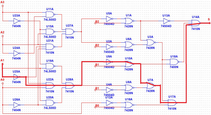
Table 4 illustrates the stage effort calculated for each logic gate, which is related to the type of logic gate and the number of branches connected to it [10].
Table 4: g for different gates | |||||||
number of inputs | |||||||
Gate Type | 1 | 2 | 3 | 4 | 5 | n | |
Inverter | 1 | ||||||
NAND | 4/3 | 5/3 | 6/3 | 7/3 | (n+2)/3 | ||
NOR | 5/3 | 7/3 | 9/3 | 11/3 | (2n+1)/3 | ||
Gate Type | Parasitic delay | ||||||
Inverter | Pinv | ||||||
n-input NAND | npinv | ||||||
n-input NOR | npinv | ||||||
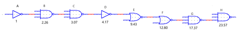
Use the formulas below to caculate the size of each gate in the critical path, shown in figure 4.
\( G=\prod _{i=1}^{8}{g_{i}}=g_{inv}^{2}×g_{3NAND}^{4}×C_{2NOR}^{2}={(\frac{5}{3})^{6}},H=32,B=1 \) (12)
\( F=GBH=685.87,f={F^{\frac{1}{N}}}=2.262,{C_{in}}=g\frac{{C_{out}}}{f} \) (13)
|
Figure 4: The size of each gate in the critical path |
3.2. Power Consumption Analysis
Power consumption is another critical consideration in modern digital circuit design. With the advancement of integrated circuit technology, low-power design has become a prevalent trend. Power consumption primarily consists of static power consumption and dynamic power consumption, with dynamic power consumption dominating in most applications.
Assume that Vth=0.2V, the formulas for calculating power consumption are as follows:
\( D=\frac{K{V_{DD}}}{{({V_{DD}}-{V_{TH}})^{2}}} \) (14)
\( 1.5D=\frac{KV_{DD}^{opt}}{{(V_{DD}^{opt}-{V_{TH}})^{2}}} \) (15)
\( E={C_{L}}V_{DD}^{2}=105.67 \) (16)
\( {E_{opt}}={C_{L}}V_{DD}^{{opt^{2}}}=63.48 \) (17)
3.3. Impact of Supply Voltage and Input Capacitance
Analysis revealed that reducing the supply voltage can effectively decrease power consumption; however, it may also lead to an increase in delay. To find a balance between delay and power consumption, the effects of different supply voltage settings and input capacitance values on circuit performance were explored. Increasing input capacitance can reduce delay but may result in higher power consumption. Therefore, it is essential to consider the relationship between these two factors comprehensively during the design process to achieve optimal performance.
3.4. Optimization Strategies
To further optimize delay and power consumption, calculations were performed using MATLAB.
\( {C_{in}}={x^{8}} ,{C_{in}}∈[1,2] \) (18)
\( F=\frac{685.67}{{x^{8}}}, f=\frac{2.262}{x}, {C_{out}}=f\frac{{C_{in}}}{g} \) (19)
\( {C_{ain}}={x^{8}}, {C_{bin}}={x^{7}}, {C_{cin}}={x^{6}}, {C_{din}}={x^{5}}, {C_{ein}}={x^{4}}, {C_{fin}}={x^{3}}, {C_{gin}}={x^{2}}, {C_{hin}}=x \) (20)
\( D=Nf+P=\frac{18.1}{x}+18 \) (21)
Through calculations, it was found that simultaneously adjusting sizing and VDD could achieve minimum power consumption, leading to optimal performance. The implementation of these strategies effectively improved the overall performance of the circuit, ensuring that it met functional requirements while achieving ideal delay and power consumption metrics.
3.5. Result Verification
Finally, the performance of the optimized circuit was verified using simulation tools, recording delay and power consumption data under various supply voltage and input capacitance settings. Experimental results indicate that the optimized circuit achieved significant improvements in both delay and power consumption, providing an effective reference for subsequent designs. The results are listed in Table 5.
4. Conclusion
This study conducted an in-depth analysis of the design and optimization of a 4-bit absolute value detector. Through the construction of a truth table and simplification of logic expressions, the circuit structure was optimized, utilizing NAND, NOR gates, and inverters to achieve an efficient circuit design. In the analysis of delay and power consumption, the impact of supply voltage and internal capacitance was explored, proposing solutions to reduce delay while minimizing power consumption. Experimental results demonstrate that the optimized circuit significantly reduces power consumption while maintaining performance, meeting the demands of modern circuit design. Future research may further investigate adaptability and optimization methods in different application scenarios.
References
[1]. Yuan M. An Absolute-value Detector with Threshold Comparing for Spike Detection in Brain-machine Interface[J].Journal of Physics: Conference Series,2021,2113(1).
[2]. Mario G .Simplifying Karnaugh Maps by Making Groups of Non-power-of-two Elements[J].Circuits, Systems, and Signal Processing,2022,41(10):5895-5902.
[3]. Tynymbayev S ,Mukasheva A ,Ibragimov K , et al.Analysis and Synthesis of Single-Bit Adders for Multi-Bit Adders with Sequential Transfers [J].Engineering Proceedings,2024,70(1):6-6.
[4]. Anjali K V ,Manish K ,Saurabh K , et al.Design of energy efficient domino logic circuit using lector technique[J].International Journal of Electronics,2023,110(11):2117-2135.
[5]. Ishika S ,Rajesh M .Delay Analysis of Half Subtractor using CMOS and Pass Transistor Logic[J].International Journal of Computer Applications,2016,141(12):18-22.
[6]. P P ,T P ,H N , et al.Testing of inductors using the NI Multisim simulation program[J].Journal of Physics: Conference Series,2022,2408(1):
[7]. Oscar C M ,Jacob J W ,Christer S , et al.Analysis of energy consumption bounds in CMOS current-steering digital-to-analog converters[J].Analog Integrated Circuits and Signal Processing,2022,111(3):339-351.
[8]. Burks M T ,Sakallah A K .Optimization of critical paths in circuits with level-sensitive latches[C]//Systems Technology and Architecture Division, IBM Corporation, Austin, TX;;Department of Electrical Engineering and Computer Science, The University of Michigan, Ann Arbor, MI,1994:
[9]. Park E ,Zang N ,Kim J .Delay Optimization using Path Correlation and Gate Sizing[J].ITC-CSCC :International Technical Conference on Circuits Systems, Computers and Communications,2007,
[10]. Lee D ,Beak S ,Lee Y , et al.Minimize the delay of parasitic capacitance and modeling in RLC circuit[C]//Myongji University, Yongin-si, Gyeonggi-do, Korea;;Myongji University, Yongin-si, Gyeonggi-do, Korea;;Myongji University, Yongin-si, Gyeonggi-do, Korea;;Andong National University, Andong-si, Gyeongbuk, Korea;;Myongji University, Yongin-si, Gyeonggi-do, Korea;;Jeju National University, Jeju-do, Korea;;Myongji University, Yongin-si, Gyeonggi-do, Korea,2009:
Cite this article
Wang,J. (2025). Design and Optimization of a 4-bit Absolute Value Detector. Applied and Computational Engineering,130,86-92.
Data availability
The datasets used and/or analyzed during the current study will be available from the authors upon reasonable request.
Disclaimer/Publisher's Note
The statements, opinions and data contained in all publications are solely those of the individual author(s) and contributor(s) and not of EWA Publishing and/or the editor(s). EWA Publishing and/or the editor(s) disclaim responsibility for any injury to people or property resulting from any ideas, methods, instructions or products referred to in the content.
About volume
Volume title: Proceedings of the 5th International Conference on Materials Chemistry and Environmental Engineering
© 2024 by the author(s). Licensee EWA Publishing, Oxford, UK. This article is an open access article distributed under the terms and
conditions of the Creative Commons Attribution (CC BY) license. Authors who
publish this series agree to the following terms:
1. Authors retain copyright and grant the series right of first publication with the work simultaneously licensed under a Creative Commons
Attribution License that allows others to share the work with an acknowledgment of the work's authorship and initial publication in this
series.
2. Authors are able to enter into separate, additional contractual arrangements for the non-exclusive distribution of the series's published
version of the work (e.g., post it to an institutional repository or publish it in a book), with an acknowledgment of its initial
publication in this series.
3. Authors are permitted and encouraged to post their work online (e.g., in institutional repositories or on their website) prior to and
during the submission process, as it can lead to productive exchanges, as well as earlier and greater citation of published work (See
Open access policy for details).
References
[1]. Yuan M. An Absolute-value Detector with Threshold Comparing for Spike Detection in Brain-machine Interface[J].Journal of Physics: Conference Series,2021,2113(1).
[2]. Mario G .Simplifying Karnaugh Maps by Making Groups of Non-power-of-two Elements[J].Circuits, Systems, and Signal Processing,2022,41(10):5895-5902.
[3]. Tynymbayev S ,Mukasheva A ,Ibragimov K , et al.Analysis and Synthesis of Single-Bit Adders for Multi-Bit Adders with Sequential Transfers [J].Engineering Proceedings,2024,70(1):6-6.
[4]. Anjali K V ,Manish K ,Saurabh K , et al.Design of energy efficient domino logic circuit using lector technique[J].International Journal of Electronics,2023,110(11):2117-2135.
[5]. Ishika S ,Rajesh M .Delay Analysis of Half Subtractor using CMOS and Pass Transistor Logic[J].International Journal of Computer Applications,2016,141(12):18-22.
[6]. P P ,T P ,H N , et al.Testing of inductors using the NI Multisim simulation program[J].Journal of Physics: Conference Series,2022,2408(1):
[7]. Oscar C M ,Jacob J W ,Christer S , et al.Analysis of energy consumption bounds in CMOS current-steering digital-to-analog converters[J].Analog Integrated Circuits and Signal Processing,2022,111(3):339-351.
[8]. Burks M T ,Sakallah A K .Optimization of critical paths in circuits with level-sensitive latches[C]//Systems Technology and Architecture Division, IBM Corporation, Austin, TX;;Department of Electrical Engineering and Computer Science, The University of Michigan, Ann Arbor, MI,1994:
[9]. Park E ,Zang N ,Kim J .Delay Optimization using Path Correlation and Gate Sizing[J].ITC-CSCC :International Technical Conference on Circuits Systems, Computers and Communications,2007,
[10]. Lee D ,Beak S ,Lee Y , et al.Minimize the delay of parasitic capacitance and modeling in RLC circuit[C]//Myongji University, Yongin-si, Gyeonggi-do, Korea;;Myongji University, Yongin-si, Gyeonggi-do, Korea;;Myongji University, Yongin-si, Gyeonggi-do, Korea;;Andong National University, Andong-si, Gyeongbuk, Korea;;Myongji University, Yongin-si, Gyeonggi-do, Korea;;Jeju National University, Jeju-do, Korea;;Myongji University, Yongin-si, Gyeonggi-do, Korea,2009: