


1. Introduction
Nowadays with the increasing pace of life, time management has become a more important but, in the meantime, a harder task for people. Therefore, clock, which is the most common tool used to indicate time, has quietly integrated into every aspect of people’s daily life. No matter in hospitals, workplaces or classrooms, people prefer to hang a clock on the wall, hoping the never-ending second hand can somehow push them or remind them of the significance of time. However, traditional mechanical clock is faced with inevitable accuracy problems since the movements between gears can be influenced due to gravity, fraction or foreign matter inside [1, 2]. In addition, conventional clock also requires manual work to maintain working correctly and the complexity in structure means limited functions, expertise restrictions when it comes to fixing or manufacturing [2]. Consequently, in this article, a way of designing a multi-functional clock that has time-setting, count and countdown, alarm and on-time alarm functions integrated together based on digital circuit is proposed to provide a more readable, practical, cost-effective and precise design of this kind of tool.
Many researches have been conducted to reach higher level of precision of digital clock and this idea has been expanded to the design of self-synchronizing digital communication system. However, many of them are based on abstract circuit expression. For instance, Figure 1 below illustrates the structure of a kind of digital phase-locked loop (DPLL) [3].
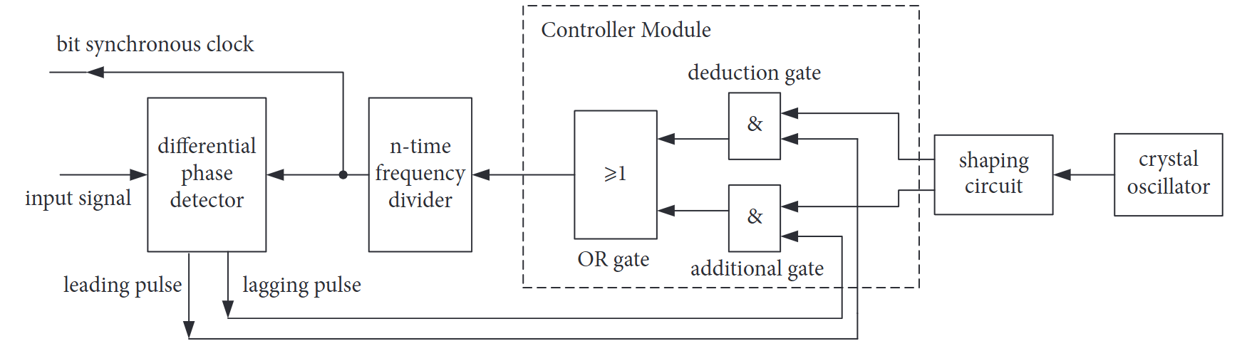
Figure 1: Structure diagram of DPLL [3]
This kind of design do make a more advanced model of clock, but meanwhile it is less user or designer-friendly. Besides, a basic clock for daily use can be more simple and easier to produce.
In this experiment, circuits were modified and tested over and over again, so the application of software simulation can possibly bring significant convenience in designing and debugging circuits compared with building real circuits. As a result, a CAD tool called NI Multisim was chosen to be applied.
NI Multisim is a free web-based platform developed by National Instruments that aims to provide significant simulation tools to revolutionize the way people study circuits [4]. In Multisim, Components including switches, 7-segment and clock signals can be found in the library, added into the circuit and have parameters modified. Once the wires are connected, press the button “run” in the “simulation” column then the simulated result can be seen on the display elements.
Therefore, this experiment intended to clarify how to build a circuit of clock from the very beginning to the final simulation and improvement. In the later part pf this article, some main components applied in design, overall circuit design and the most important concepts of clock, carry and borrow digit, will be introduced in the basic theoretical analysis part. The third part will be the build and test for circuit. After that, the discussion about further improvements and analysis will be given in the fourth part before conclusion.
2. Basic theoretical analysis
Logical or digital circuits are comprised of two main categories of basic circuit structure, the combination circuits and sequential circuits. Sequential circuit is a type of circuit construction which usually consists of a combinational logic part, a series of components that acts as memory like flip-flops, and previous inputs and outputs [5]. According to Figure 2 below, the combinational logical part A1 is comprised of Boolean nodes and each of the nodes represents a global Boolean function to process the inputs and get the corresponding outputs for the start of next state [5].
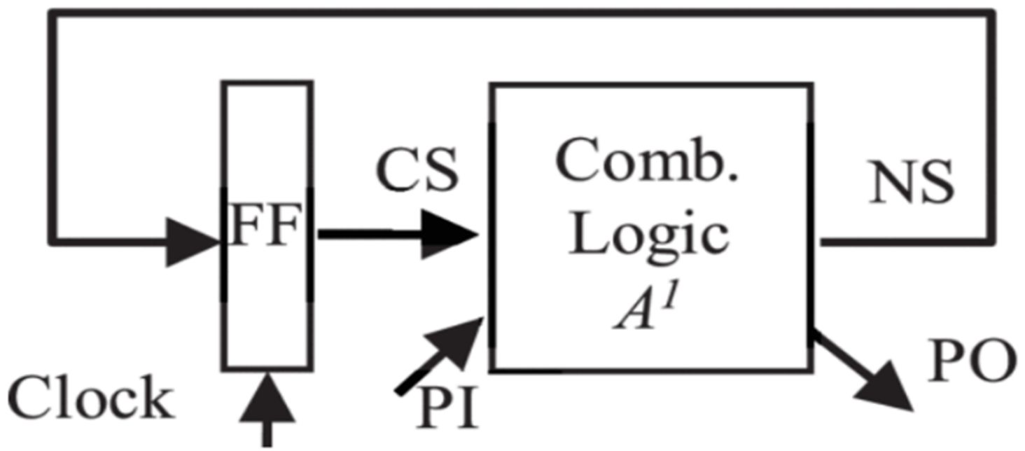
Figure 2: An example sequential circuit [5]
Generally, sequential circuits are divided into two main kinds, which are synchronous and asynchronous circuits. The main difference is that synchronous sequential circuits have clock-controlled elements [6]. According to [7], in synchronous sequential circuit, the parameters of clock signals determine the rate of data transmission within the circuit. Given this fact, if the circuit or arithmetic operations of this system can be set at the speed of one bit per second or more precise, it is possible to build a circuit of a multifunctional clock based on this structure of circuit.
2.1. Circuit overview
Figure 3 and Figure 4 below are the circuits for time-setting, count, countdown part and alarm, on-time alarming part respectively. They should be integrated together using shared 7-segment display but for readability, this article will separate the whole circuit into two main parts in further illustration.
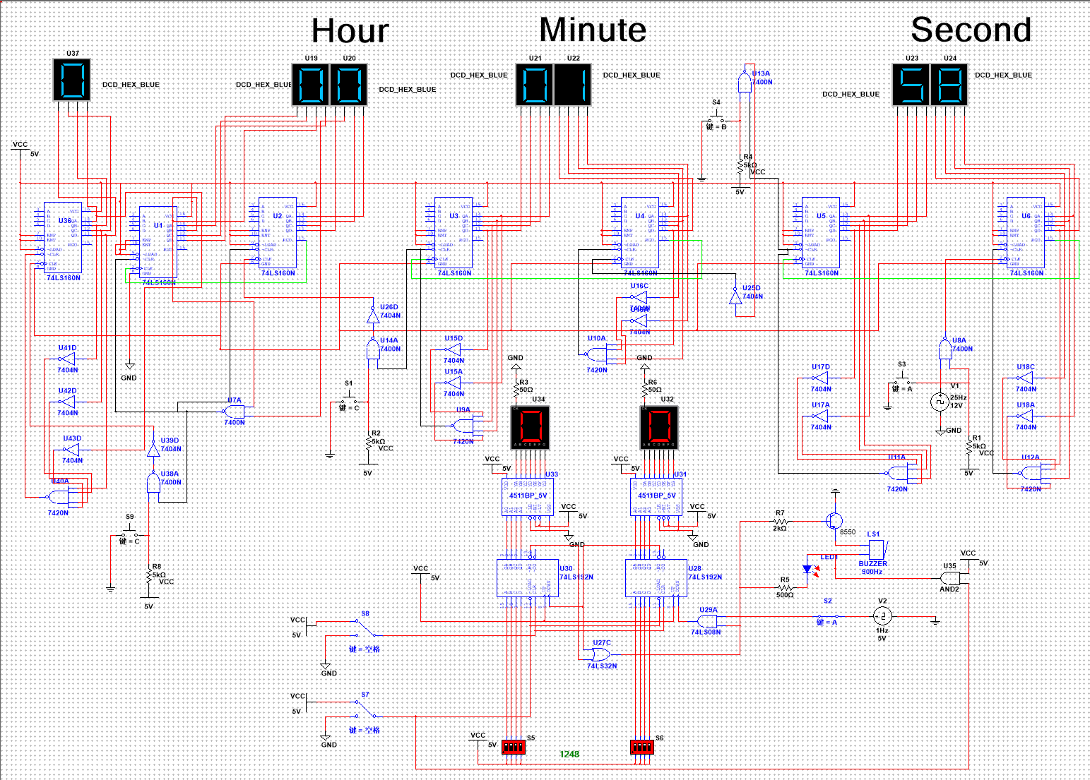
Figure 3: Circuit for time-setting, count and countdown functions (Photo/Picture credit: Original)
In the circuit in Figure 3, the top four sets of 7-segment were set to represent day, hour, minute and second from left to right. Key S9, S1, S4 and S3 were four switches for manual time-adjustment of the corresponding four values. Switch sets S5 and S6 were applied to pre-set the countdown time. S7, S8 were used to start or clear the countdown time and key S2 was to realize pause in this process. These functions were conducted by chips 74LS160N and 74LS192N, which were applied to accomplish carry digit and borrow digit according to time signal.
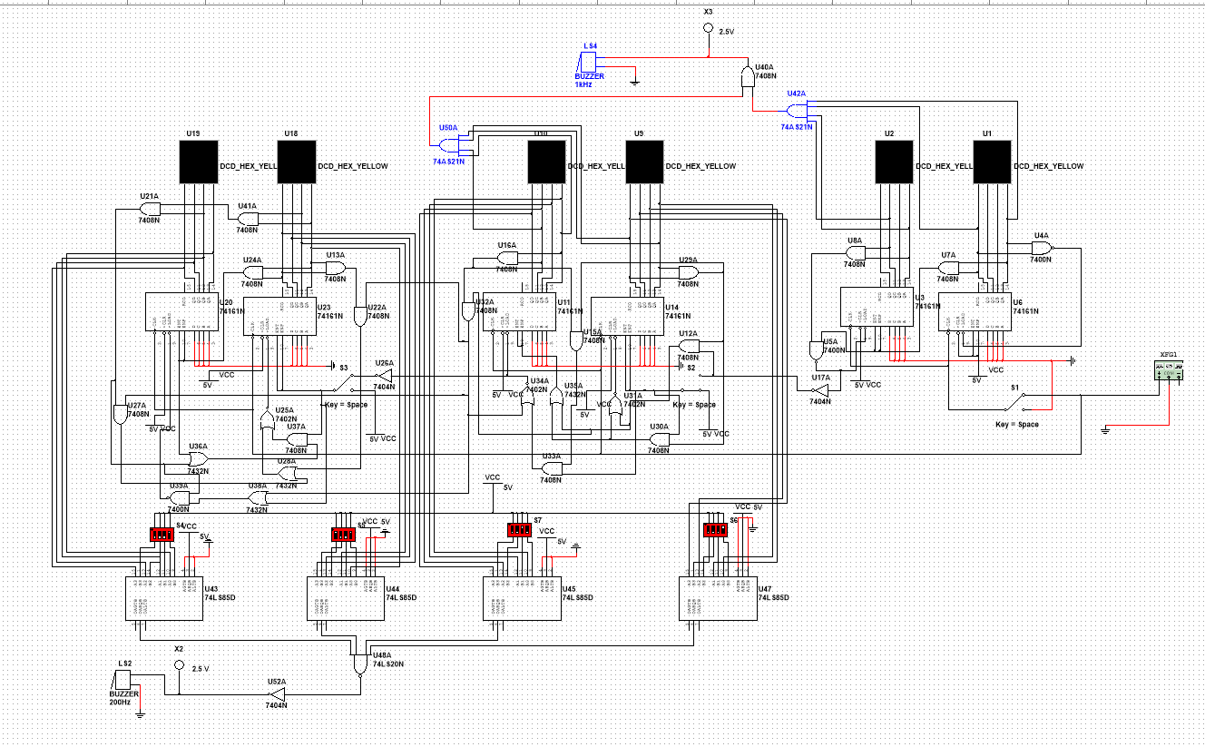
Figure 4: Circuit for alarm and on-time alarm functions (Photo/Picture credit: Original)
Figure 4 for one thing was the realization of alarm part of the clock, with switch sets below applied to set the alarm time and the red part at the very top for on-time alarming based on chip 74LS85D. For another, it provided an improved version of the basic clock structure since the chips in circuit won’t work until time signal is received, which contributes to the energy-saving attribute in this design.
2.2. Main components
In the previous section, three main types of chips were mentioned, which were 74LS160N, 74LS192N and 74LS85D. The first two of them were to conduct the most basic principle of clock, which are carry digit and borrow digit while 74LS85D was selected to realize the function of alarm clock. In the following part, all the three chips will be introduced respectively.
74LS160D is a kind of counter that use four-bit binary output to generate output from 0000 to 1001 (0~9). ABCD are four-bit input of the chip, which determines from which number the counter starts to add number. QA, QB, QC and QD are four corresponding output ports. ENP and ENT are two pins used to choose working mode, commonly set to high voltage both. ~LOAD and ~CLR enable the chip to be activated by an addition signal LOAD and to be reset asynchronously (set to 0000) when CLR is low. CLK is where 74LS160D receives clock signal. When rising edge is detected in this port, the number stored in the counter will plus one. After 1001 is added by one, output will return to 0000 and RCO will generate a positive pulse to represent a carry digit [8].
74LS192N is an advanced version of 74LS160D. Similarly, 74LS192N also has pins ABCD and QA, QB, QC and QD set as input and output ports as well as LOAD and CLR function. What differs it with 74LS160D is that 74LS192N is a type of reversible chip, which means that it can not only conduct carry digit operation, but can also cope with borrow digit situations. When clock signal is attached to UP, it is totally the same as 74LS160D with ~CO output acts as carry digit output. However, when DOWN serves as the input port for time signal, the number stored decreases by one at every rising edge of time signal, and ~BO will generate a negative pulse when 0000 will decrease [9].
74LS85D is not a counter as the previous two components. This chip commonly acts as comparator in circuits, which, as its name indicates, is used to compare two inputs and then give the output to represent results of corresponding comparison. A3~A0 and B3~B0 are two four-bit binary input wait to be compared. AGTB (A Greater Than B), AEQB (A Equals B) and ALTB (A Less Than B) are three input ports to decide what is compared. Naturally, OAGTB, OAEQB and OALTB are three output pins for the choosing comparison. For example, if AEQB is set high, then the chip will find out whether A equals B. If so, the OAEQB will be 1 and 0 if not, leaving the other two output pins OAGTB and OALTB no exact output [10]. The Pin map for 74LS160D, 74LS192N and 74LS85D is shown in Figure 5.
The pin map of 74LS160D is shown in Figure 5.
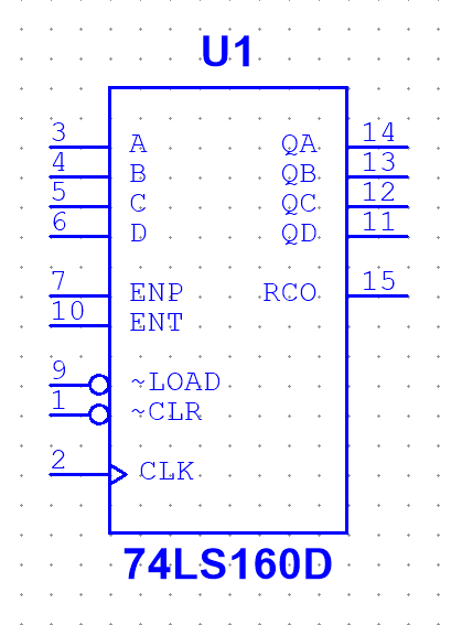
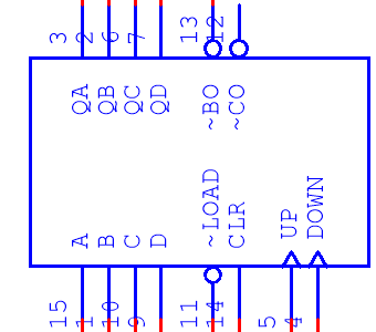
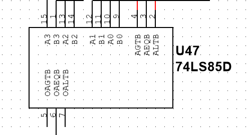
Figure 5: Pin map for 74LS160D, 74LS192N and 74LS85D [8-10]
3. Circuit construction and testing
Due to the fact that circuits for different functions were integrated together, in order to ensure readability, five functions will be introduced separately in this part, which are counting, time-setting, countdown, alarm and on-time alarm.
3.1. Counting
Counting is the most fundamental function a clock should have. The key to realize this functionality is to set to base-60 and base-24 in the circuit since HOUR and MINUTE requires 60 minutes and 60 seconds to plus one and DAY requires 24 to plus one. Now, the design of SECOND will be illustrated and that is similar to that of MINUTE.
The outputs of two 74LS160N were connected to two 7-segments to represent the 00~59 seconds. Besides, the binary number should be read form D to A. The basic idea was every time U6 is 1010, is should be reset to 0000 and U5 should plus one simultaneously. U5, however, should be reset every time it is 0110 and then produce a carry digit to MINUTE part. Realization of SECOND is shown in Figure 6.
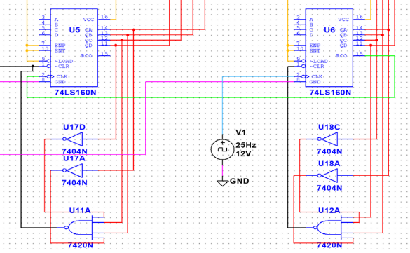
Figure 6: Realization of SECOND (Photo/Picture credit: Original)
Since it has been mentioned that CLR activates when it turns to low voltage, so for U6, two NOT gates and one 4-input NAND gate were applied to set the input at CLR of U6 to be \( \overline{\bar{A}B\bar{C}D} \) , which only produces 0 when DCBA is 1010 (10). Similarly, as for U5, the connection of two NOT gates and NAND gate aimed to set a \( \overline{A\bar{B}\bar{C}D} \) at CLR, which only produces 0 when DCBA is 0110 (6).
As for MINUTE, it was almost the same as SECOND part because both of them are base-60. Therefore, more stress will be put on the realization of HOUR.
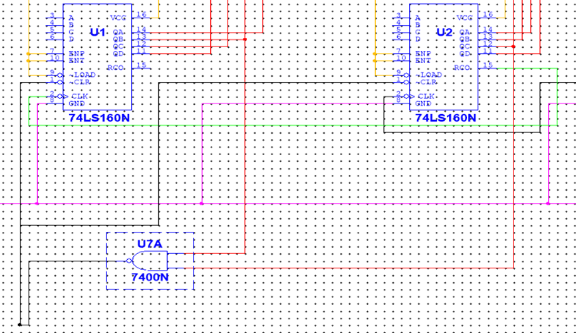
Figure 7: Realization of HOUR (Photo/Picture credit: Original)
As Figure 7 shows, unlike MINUTE and SECOND, HOUR needed to be reset when it turns to 24, which in U1 and U2 is represented as 0010 and 0100. As a result, not all the output pins were necessary to be used to form the CLR signal. Given the idea mentioned before, only the QB of U1 and QC of U2 were required to enter the NAND gate to generate the CLR signal. In this case, no carry digit output was produced so when it comes to the connection between HOUR and DAY, according to Fig.3, it was the output of NAND gate U7A rather than that of CO that acted as the CLK for DAY part.
3.2. Time-setting
Previous section has introduced the basic model of a clock. However, the system seemed can only start counting from 0 Day 00 Hour 00 Minute 00 Second. As a result, it was necessary to guarantee that this clock can be modified manually. Here a possible way of time-setting will be discussed.
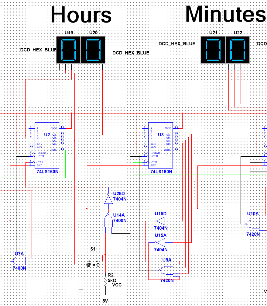
Figure 8: Circuit for time-adjustment (Photo/Picture credit: Original)
From Figure 8, take the adjustment of HOUR for example, the key S1 was put with the CLR signal of MINUTE as the input of NAND gate U14A. In normal circumstances, these two inputs were high and so as the CLK in U2. When MINUTE is cleared and CLR of U3 changes to low, the CLK of U2 changes simultaneously. Similarly, when key S1 is pressed, the high voltage is connected to ground, forming low voltage in the input port of NAND gate and forcing CLK of HOUR to change, thus realizing the adjusting of HOUR. This structure can also be replicated to accomplish time-setting for MINUTE and SECOND.
3.3. Countdown
To realize the countdown functionality, the reversible chip 74LS192N mentioned before must be applied. The basic idea was quite similar to that of counting. Circuit for countdown is shown in Figure 9.
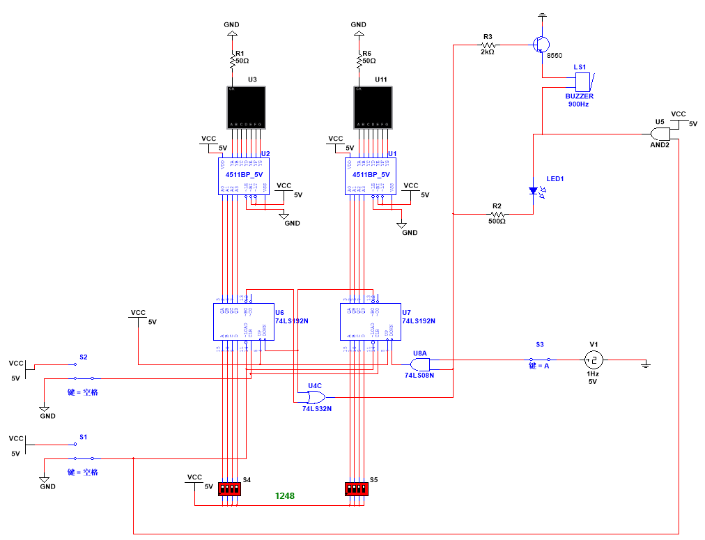
Figure 9: Circuit for countdown (Photo/Picture credit: Original)
The working principle of this circuit is that switches S4 and S5 directly pre-set the countdown time and import into 74LS192N. Then the outputs of chips were transmitted into 4511BP decoder which specifically transform binary coded decimal on successive 7-segments. U3 and U11 were designed to represent every 10 second and every second. As the number in U7 decreases to 0000, a digit is needed from higher 10 second U6 for U7 to return to 1001. As a result, ~BO port of U7 was attached to DOWN of U6, making number in U6 subtracted by one. Key S3 was placed between DOWN of U7 and clock signal to pause the process. When it is opened, no clock signal input means the system will remain the state until S3 is closed again.
To ensure more practicability, an alarming part with buzzer and LED was added as well. When the countdown is over, which means both ~BO ports are 0, the output of OR gate will be 0. AND gate U5 was set to ensure the alarming system will not work unless the system is started (LOAD is 1) since time-setting goes first and the initial state is 00 second, which will just activate the alarming system.
3.4. Alarm and on-time alarm
Alarm and on-time alarm were additional functionalities integrated on basic clock circuit. Figure 10 below illustrates the main function area of alarm.
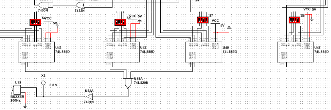
Figure 10: Function circuit for alarm (Photo/Picture credit: Original)
Alarm is a kind of tool that provides warning when the present time is equal to the setting time. So, four comparators 74LS85D were applied and were set to AEQB mode, which aims to judge whether input A is equal to input B. From the circuit, four input B were decided by switches S4~S7 and four input A were the output from the counters. When it is the time to alarm, four OAEQB output will be 1 and after a NAND and NOT gate, it turns out to be high voltage. Due to another port of buzzer has been grounded, this situation allows buzzer and LED to work, which meet with the expectations.
On-time alarm was relatively simple since the only requirement was ensure a high voltage at every 59 minutes 59 seconds (0101 1001 0101 1001). Based on the similar idea mentioned in III. 1, it can be attained by two four-input AND gates and one AND gates. Function circuit for on-time alarm is shown in Figure 11.
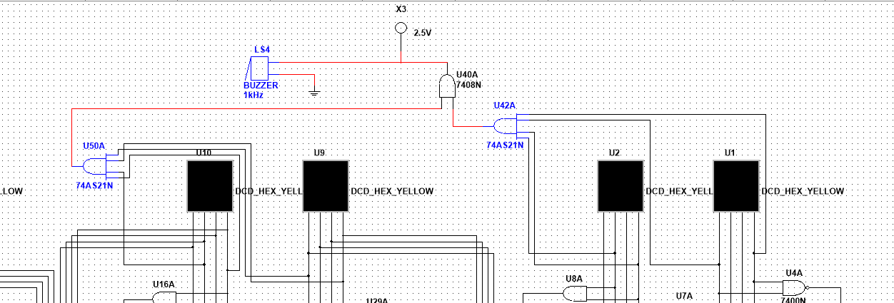
Figure 11: Function circuit for on-time alarm (Photo/Picture credit: Original)
4. Improvements and further analysis
To start with, this experiment mainly focused on the theoretical part of the circuit design and the circuits were all built and tested or simulated on CAD tool rather than integrated on real circuit board. It is still unknown whether these kinds of circuit construction are easy or difficult to realize in actual manufacturing circumstances. Therefore, it is suggested that these designs can be applied and examined in reality.
Nowadays, there are multiple choices about the counter or comparator of different types or from different manufacturers. As for a small integrated system, it is worth considering about the energy-consumption or heat accumulation problems. It is also beneficial for later circuit designers to take efficiency issue into consideration.
In addition, apart from the five basic capabilities mentioned in this article, there are far more aspects that worth more attention and are useful as well in real situations. For example, if the clock is integrated into lighting system, it is possible to create a intelligent light whose light intensity can modify automatically according to time or photosensitive sensors. Besides, wireless modules or voice recognition function can also be applied to create a more convenient clock.
Finally, in this experiment, the clock signal was generated by a 1kHz AC voltage, which is real situation can be realized by combining timer, capacitors and inductors to build oscillating circuit. However, this may not precise enough since researches have figured out solutions like using the atomic clock or the DPLL mentioned before to attain more precise clock signals [3, 11]. If these methods are applied, the clock can be applied to more fields in which time matters.
5. Conclusion
In conclusion, this experiment successfully demonstrated the design and simulation of a multifunctional digital clock circuit using sequential circuits. By employing components like counters, reversible counters, and comparators, the clock integrated practical functions such as time-setting, countdown, alarm, and on-time alert. The simulation conducted in NI Multisim confirmed the reliability of the design, fulfilling all intended functions. Despite the constraints of this virtual setup, the experiment highlights valuable directions for future development. Enhancements in energy efficiency, real-world applicability, and precision timing methods, such as atomic clocks, would be beneficial for extending the clock's potential applications. This project underlines the feasibility and versatility of sequential circuits for digital timekeeping solutions, paving the way for further innovations in digital clock design.
References
[1]. Van Rossum G D. The Oxford Handbook of Early Modern European History, 1350-1750: Volume I: Peoples and Place. Oxford Handbooks, 2015, 5, 145-164.
[2]. Lombardi M A. First in a series on the evolution of time measurement: Celestial, flow, and mechanical clocks [Recalibration]. IEEE Instrumentation & Measurement Magazine, 2011, 14(4): 45-51.
[3]. Duan H, Huang H, Li C. Improved Design of Bit Synchronization Clock Extraction in Digital Communication System. Journal of Electrical and Computer Engineering, 2018, 2018(1): 8024168.
[4]. Mitolo M. Simulation-based Labs for Circuit Analysis: Discovering Circuits with Multisim Live and Tinkercad. CRC Press, 2024.
[5]. Savoj H, Mishchenko A, Brayton R. m -Inductive Property of Sequential Circuits. IEEE Transactions on Computer-Aided Design of Integrated Circuits and Systems, 2024, 35(6), 919-930.
[6]. Nishimura S. Classification of Sequential Circuits as Causal Functions. arXiv preprint arXiv:2306.17583, 2023.
[7]. Farrahi A H, Chen C, Srivastava A, et al. Activity-driven clock design[J]. IEEE Transactions on Computer-Aided Design of Integrated Circuits and Systems, 2001, 20(6): 705-714.
[8]. SN74LS160AD Datasheet. Texas Instruments, 2024. https://www.alldatasheet.com/datasheet-pdf/pdf/27415/TI/SN74LS160AD.html
[9]. SN74LS192N Datasheet. Texas Instruments, 2024. https://www.alldatasheet.net/datasheet-pdf/pdf/85760/TI/SN74LS192N.html
[10]. SN74LS85D Datasheet. Texas Instruments, 2024. https://www.alldatasheet.com/datasheet-pdf/pdf/27436/TI/SN74LS85D.html
[11]. Hinkley N, Sherman J A, Phillips N B, et al. An atomic clock with 10–18 instability. Science, 2013, 341(6151): 1215-1218.
Cite this article
Zhou,Y. (2025). The Application Analysis of Sequential Circuit in the Design of Multifunctional Clock. Applied and Computational Engineering,130,216-225.
Data availability
The datasets used and/or analyzed during the current study will be available from the authors upon reasonable request.
Disclaimer/Publisher's Note
The statements, opinions and data contained in all publications are solely those of the individual author(s) and contributor(s) and not of EWA Publishing and/or the editor(s). EWA Publishing and/or the editor(s) disclaim responsibility for any injury to people or property resulting from any ideas, methods, instructions or products referred to in the content.
About volume
Volume title: Proceedings of the 5th International Conference on Materials Chemistry and Environmental Engineering
© 2024 by the author(s). Licensee EWA Publishing, Oxford, UK. This article is an open access article distributed under the terms and
conditions of the Creative Commons Attribution (CC BY) license. Authors who
publish this series agree to the following terms:
1. Authors retain copyright and grant the series right of first publication with the work simultaneously licensed under a Creative Commons
Attribution License that allows others to share the work with an acknowledgment of the work's authorship and initial publication in this
series.
2. Authors are able to enter into separate, additional contractual arrangements for the non-exclusive distribution of the series's published
version of the work (e.g., post it to an institutional repository or publish it in a book), with an acknowledgment of its initial
publication in this series.
3. Authors are permitted and encouraged to post their work online (e.g., in institutional repositories or on their website) prior to and
during the submission process, as it can lead to productive exchanges, as well as earlier and greater citation of published work (See
Open access policy for details).
References
[1]. Van Rossum G D. The Oxford Handbook of Early Modern European History, 1350-1750: Volume I: Peoples and Place. Oxford Handbooks, 2015, 5, 145-164.
[2]. Lombardi M A. First in a series on the evolution of time measurement: Celestial, flow, and mechanical clocks [Recalibration]. IEEE Instrumentation & Measurement Magazine, 2011, 14(4): 45-51.
[3]. Duan H, Huang H, Li C. Improved Design of Bit Synchronization Clock Extraction in Digital Communication System. Journal of Electrical and Computer Engineering, 2018, 2018(1): 8024168.
[4]. Mitolo M. Simulation-based Labs for Circuit Analysis: Discovering Circuits with Multisim Live and Tinkercad. CRC Press, 2024.
[5]. Savoj H, Mishchenko A, Brayton R. m -Inductive Property of Sequential Circuits. IEEE Transactions on Computer-Aided Design of Integrated Circuits and Systems, 2024, 35(6), 919-930.
[6]. Nishimura S. Classification of Sequential Circuits as Causal Functions. arXiv preprint arXiv:2306.17583, 2023.
[7]. Farrahi A H, Chen C, Srivastava A, et al. Activity-driven clock design[J]. IEEE Transactions on Computer-Aided Design of Integrated Circuits and Systems, 2001, 20(6): 705-714.
[8]. SN74LS160AD Datasheet. Texas Instruments, 2024. https://www.alldatasheet.com/datasheet-pdf/pdf/27415/TI/SN74LS160AD.html
[9]. SN74LS192N Datasheet. Texas Instruments, 2024. https://www.alldatasheet.net/datasheet-pdf/pdf/85760/TI/SN74LS192N.html
[10]. SN74LS85D Datasheet. Texas Instruments, 2024. https://www.alldatasheet.com/datasheet-pdf/pdf/27436/TI/SN74LS85D.html
[11]. Hinkley N, Sherman J A, Phillips N B, et al. An atomic clock with 10–18 instability. Science, 2013, 341(6151): 1215-1218.