


1. Introduction
The new era of high-speed communication and the increasing demand for higher stability in chips present significant challenges for the next generation of on-chip power modules. The internal power management of integrated circuits and the expansion of device sizes have become increasingly challenging. Low dropout regulators (LDOs) are widely used in communication chips to power various modules due to their advantages of low noise and good load/line regulation. On-chip LDOs eliminate large output capacitors, accelerate the manufacturing process, and are thus favored in modern designs[1][2][3][4][5]. However, due to the absence of large output capacitors to absorb output voltage (VOUT) spikes, the transient performance of on-chip LDOs is crucial [6]. In the transmitter (TX) section of SerDes (Serializer/Deserializer), LDOs are typically used to provide a stable, low-noise power supply voltage to support high-performance data transmission. SerDes generally operate in the GHz frequency range and experience significant current fluctuations under high-speed switching conditions. LDOs with good transient performance maintain a stable output voltage when the load changes rapidly, reducing power noise in both the transmitter and receiver sections of the SerDes circuit, which is extremely helpful for improving the output eye diagram. In summary, LDOs with high precision and fast transient response play a crucial role in communication interface circuits [7].
This paper proposes an LDO with high loop gain based on adaptive dynamic biasing, implemented using 12nm CMOS technology. The bias current of the loop error amplifier in the proposed LDO dynamically adjusts with the load, and a current-sampling-based transient response enhancement technique is employed to quickly compensate for load current changes when the LDO experiences sudden load fluctuations. The proposed LDO can accommodate a wide range of load capacitances, achieving high stability, fast transient response, and minimal voltage spikes when the load capacitance is between 0 and 100pF. In the first section, we introduce the architecture, implementation, and operating principles of the proposed LDO. Detailed test results are reported in the second section, and conclusions are provided in the third section.
2. LDO Circuit Design
2.1. Overall Circuit Design
Figure 1 shows the proposed analog LDO circuit. It employs adaptive dynamic biasing, with transistor M4 mirroring the current of Mp. The sizes of transistors M4、M5、M6, and M7 are designed to be equal. Transistors M3、M2、M5、M6、M8, and M3 form a negative feedback loop, while transistors M3、M1、M4、M7、M9, and M3 form a positive feedback loop. Stability is achieved by ensuring that the overall negative feedback loop gain, which includes the negative feedback loop formed by M1、M4、Mp、R1, and M2, is always greater than the gain of the positive feedback loop.
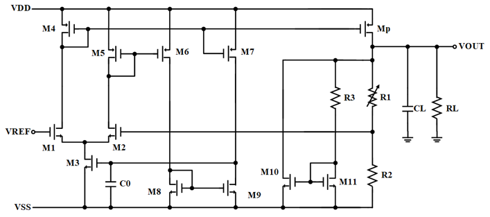
Figure 1: Proposed Analog LDO Circuit
2.2. High Precision Implementation
After organizing, the following expression can be obtained:
\( {A_{V,open\_loop}}=\frac{1}{2}\frac{{(\frac{W}{L})_{P}}}{{(\frac{W}{L})_{4}}}{g_{m1}}{R_{2}}(1+{g_{m3}}({r_{o7}}||{r_{o9}})) \)
\( {A_{V,closed\_loop}}=\frac{\frac{1}{2}\frac{{(\frac{W}{L})_{P}}}{{(\frac{W}{L})_{4}}}{g_{m1}}{R_{2}}(1+{g_{m3}}({r_{o7}}||{r_{o9}}))}{1+\frac{1}{2}\frac{{(\frac{W}{L})_{P}}}{{(\frac{W}{L})_{4}}}{g_{m1}}{R_{2}}(1+{g_{m3}}({r_{o7}}||{r_{o9}}))} \)
The above equations represent the low-frequency open-loop and closed-loop gains of the LDO core. In the design of the operational amplifier, the tail current source transistor M3 participates in the amplification process, providing a gain of \( \frac{1}{2}\frac{{(\frac{W}{L})_{P}}}{{(\frac{W}{L})_{4}}}{g_{m1}}{R_{2}}(1+{g_{m3}}({r_{o7}}||{r_{o9}})) \) at low frequencies. This significantly improves the open-loop gain of the proposed LDO.
In the proposed LDO design, the grounded capacitor C0 acts as a compensation capacitor, playing a critical role in the system's stability. Through the analysis of the system's response, it is found to exhibit the characteristics of a second-order low-pass filter. In this LDO circuit, two key poles exist. The primary pole is located at the gate of transistor M3, and its corresponding frequency is:
\( {ω_{p0}}=\frac{1}{{C_{0}}({r_{o7}}||{r_{o9}})} \)
The secondary pole appears at the LDO output node, with a frequency of:
\( {ω_{p1}}=\frac{1}{{C_{L}}[{r_{oP}}||({R_{1}}+{R_{2}})||{R_{L}}]} \)
To ensure system stability and good phase margin, we focus on the relative positioning of the primary and secondary poles. By carefully designing the size of the compensation capacitor C0, and particularly by adjusting C0 at the gate of M3, even under light load conditions, the frequency position of the secondary pole will not adversely affect the primary pole. This design strategy ensures that the phase margin of the system remains within a good range, thereby significantly improving the dynamic stability of the LDO.
Furthermore, the advantage of this compensation method lies not only in its application to the specific parameter combination in the current design but also in its broader applicability. By appropriately adjusting the value of C0, the design can be adapted to different load conditions and process parameters, thereby enhancing the robustness and reliability of the LDO circuit design [8].
2.3. Adaptive Dynamic Biasing Technology
The proposed LDO design adopts an adaptive dynamic biasing technique that significantly improves the transient response performance of the LDO. This technique dynamically adjusts the internal bias currents and voltages of the circuit to achieve a fast response to output voltage fluctuations [9]. When the output voltage Vout drops, it first results in a decrease in the gate voltage of transistor M2. This change directly causes a reduction in the pull-down current of M2, triggering a series of dynamic adjustment mechanisms.
Specifically, through the current mirror structure formed by M5 and M6, the change in the pull-down current is passed to the next stage, causing a response in the mirror structure formed by M8 and M9. This eventually leads to an increase in the gate voltage of M3. This change further increases the current through M1, enhancing the supply capability to the load and suppressing the downward trend of the output voltage.
To further improve the speed and accuracy of the transient response, we designed a current mirror structure consisting of transistor M4 and the power transistor Mp. When the current flowing through M4 increases, this current mirror structure quickly adjusts the bias current of Mp, accelerating its dynamic response capability. This design enables the output voltage Vout to quickly increase and return to the target level, significantly shortening the transient response time.
Moreover, the advantage of adaptive dynamic biasing is not only reflected in its fast transient recovery capability but also in its adaptability to different load conditions. By carefully optimizing the dimensions and biasing parameters of key devices such as M2, M3, and M4, dynamic performance can be balanced between light and heavy loads, providing a more stable and efficient operating foundation for the LDO.
2.4. Current Sampling-Based Transient Response Enhancement Technique
Furthermore, this paper proposes a current-sampling-based transient response enhancement technique to significantly improve the dynamic performance of the LDO under rapid load variation conditions. This technique consists of a resistor R3 and transistors M10 and M11, and features a simple and efficient structure. It significantly improves the LDO's transient response characteristics while saving chip area.
Specifically, when the load current suddenly decreases, the output voltage Vout of the LDO will rise rapidly due to transient effects. This change causes an increase in the current flowing through resistor R3. Since M10 and M11 form a current mirror structure, the change in current flowing through M10 is given by:
\( {i_{ds10}}=\frac{{(\frac{W}{L})_{10}}}{{(\frac{W}{L})_{11}}}\frac{{v_{out}}}{{R_{3}}+\frac{1}{{g_{m11}}}} \)
In this expression, the increase in current flowing through M10 compensates for the decrease in load current, thus stabilizing the LDO output voltage. Conversely, when the load current suddenly increases, Vout will show a downward trend, leading to a decrease in the sampling current flowing through R3. Under the current mirror mechanism, the current flowing through M10 will also decrease, compensating for the change in load current.
The proposed LDO incorporates both adaptive dynamic biasing and transient response enhancement techniques, which significantly reduce the variation in output voltage and recovery time during load changes, optimizing the slew rate.
Finally, the output node of the proposed LDO uses a variable resistor voltage divider. We designed a variable resistor divider with resistors R1 and R2, so that:
\( {V_{OUT}}=\frac{{R_{1}}+{R_{2}}}{{R_{2}}}{V_{REF}} \)
By adjusting the size of R1, the output voltage of the LDO can be raised or lowered, thereby ensuring stable power supply to other modules in the chip under different PVT (Process, Voltage, and Temperature) conditions.
3. Simulation and Test Results
The proposed LDO is fabricated using a 12nm process and exhibits significant advantages in both technical specifications and practical performance. The effective area of the LDO is 0.004 mm², and this compact area includes an on-chip load capacitor CL with a capacitance value of 45pF. The small on-chip capacitor provides a significant area advantage for the LDO. The chip cross-section and layout of the proposed LDO are shown in Figure 2. The selection of the on-chip capacitor CL is an important trade-off in the LDO design. A smaller CL can significantly reduce the chip area, thereby improving chip integration and cost-effectiveness. However, the drawback is that it may weaken the load transient response ability, leading to a deterioration in dynamic performance. Conversely, selecting a larger CL can enhance the transient response characteristics, but it occupies more chip area and, due to the larger capacitance, limits the bandwidth (BW) of the feedback loop, which may negatively impact the overall performance of the design. Therefore, a balance must be considered between transient response speed and chip area in the design to meet practical application requirements. Figure 3 shows the transient behavior of the LDO output voltage when the load current jumps from 100µA to 30mA, and vice versa, with and without the current-sampling-based transient response enhancement technique, at a supply voltage of 1.8V and a reference voltage of 0.8V. Figure 4 shows the power supply rejection ratio (PSR) curve of the proposed LDO.
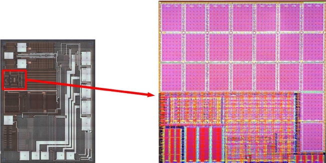
Figure 2: Cross-sectional and layout diagram of the proposed LDO.
3.1. Transient Response Test
During testing, the load current of the LDO suddenly changes from 100µA to 30mA, and then from 30mA back to 100µA. Both transitions have a rise time and fall time of 1µs. Under this dynamic load condition, the traditional LDO, which does not use the transient response enhancement technique, exhibits a 31.9mV undershoot during load rise and a 27.5mV overshoot during load drop. This large undershoot and overshoot reflect the limitations of traditional LDOs, which have slower response speeds and insufficient adjustments under rapid load changes.
In contrast, the proposed LDO, by employing the current-sampling-based transient response enhancement technique, significantly optimizes transient performance. Under the same test conditions, the output voltage of the LDO exhibits only a 5.8mV undershoot and a 7.6mV overshoot, reducing the undershoot and overshoot amplitudes by approximately 81.8% and 72.4%, respectively, compared to the traditional design, as shown in Figure 3.
This result indicates that the current-sampling-based transient response enhancement technique can effectively improve the LDO's response to load transients. Specifically, the technique dynamically adjusts the compensation current to quickly balance the output voltage fluctuations caused by load current variations, significantly improving the LDO's stability and transient performance. This improvement not only enhances the accuracy of the output voltage but also reduces the risk of system performance degradation due to undershoot or overshoot, making it especially suitable for applications requiring high voltage accuracy and dynamic stability.
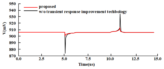
Figure 3: Transient response performance of the proposed LDO.
Test results show that when the load switches from light load to heavy load, the rise rate (slew rate) of the output voltage is 2mV/µs, while when the load switches from heavy load to light load, the fall rate of the output voltage reaches 6.08mV/µs. These rise and fall rates not only demonstrate the LDO's fast response capability to load transients but also highlight the technical advantages of the proposed design in achieving high dynamic performance.
3.2. Loop Gain and Power Supply Rejection Ratio
From the loop characteristics, the proposed LDO achieves a loop gain of 114dB in the low-frequency range, with a phase margin of 70 degrees. This combination of high gain and phase margin ensures the LDO's excellent stability under a wide range of load and power supply variations. Additionally, under light load conditions, the phase margin decreases slightly but remains at 52 degrees, which is still sufficient to support stable loop operation.
The optimization of both low and high-frequency loop gain not only enhances the LDO's stability but also has a significant impact on its power supply rejection ratio (PSR) performance. The proposed LDO achieves a PSR of -105dB in the low-frequency range, indicating its ability to significantly suppress power supply noise and ensure the purity of the output voltage. This performance is particularly important in noise-sensitive analog circuits. Furthermore, the PSR of this LDO remains above -8dB across the entire frequency range, as shown in Figure 4. This efficient power supply noise suppression capability over a wide frequency range lays a solid foundation for the LDO’s application in various complex operating environments.
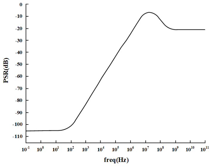
Figure 4: PSR curve of the proposed LDO.
3.3. Comparison with Other LDO Architectures
Table I summarizes the results and compares the proposed LDO with other architectures. The proposed LDO achieves the best transient characteristics among similar designs while maintaining high precision. The figure of merit (FOM) of the regulator is 1.3e-7 (the smaller the FOM number, the better). By using PMOS as the power transistor, the proposed LDO incorporates self-biasing and transient response enhancement techniques, resulting in a simple and efficient design.
Table 1: Performance Comparison
[10] | [11] | [12] | [13] | [14] | This work | |
Year | 2017 | 2022 | 2016 | 2016 | 2015 | 2024 |
Technology(nm) | 22 | 28 | 500 | 90 | 65 | 12 |
VIN(V) | 2.0 | 0.6-1 | 2.3-5.5 | 1.2-2.5 | 1.15-1.4 | 1.6-2 |
VOUT(V) | 0.77 | 0.5-0.9 | 1.2-5.4 | 1 | 0.95-1.2 | 0.81-0.99 |
Imax(mA) | 15 | 1500 | 150 | 100 | 50 | 30 |
COUT(pF) | 30 | 0.005 | — | — | 140 | 45 |
DC_gain@I=Imax(dB) | 55 | 80 | 159 | 46 | 50 | 114 |
PSR(dB) | -35@10MHz | -20@1MHz | -58@10kHz | -70@100kHz | -12@5MHz | -102@10kHz |
Active Area(mm²) | 0.02 | 0.048 | 0.279 | 0.004 | 0.026 | 0.004 |
FOM(mm²*µs*mV/(dB²*mA)) | 1.64e-4 | 6e-8 | 4.3e-5 | 7.4e-7 | 4.7e-5 | 1.3e-7 |
Note: “—” indicates no data available.
\( FOM=\frac{Area×∆t×∆{V_{OUT}}}{D{C_{gain}}×|PSR|×∆{I_{OUT}}} \)
4. Conclusion
This paper proposes a high-loop gain LDO with fast transient response based on a self-biasing circuit. The LDO is capable of supporting a maximum load current of 30mA. It employs a current-sampling transient response enhancement technique, which significantly reduces the output voltage overshoot and undershoot. Specifically, when the load current rapidly switches, the LDO’s output voltage undershoot is only 5.8mV, and the overshoot is only 7.6mV. The tail current source contributes to the amplification, resulting in a loop gain of 114dB. This LDO has been implemented in a 12nm CMOS process and demonstrates satisfactory performance.
Author Information:
Liu Weihan (2000–), male (Han ethnicity), from Hefei, Anhui, master’s student, engaged in analog integrated circuit design;
Chen Xiaofei (corresponding author), female (Han ethnicity), associate professor, E-mail: xfchen@hust.edu.cn.
Funded Projects
National Natural Science Foundation of China (No. U22A2083);
HUST (Huazhong University of Science and Technology) Independent Innovation Fund (HUST: 2023JCYJ040);
Innovation Research Project of Hubei Optics Valley Laboratory (No. OVL2024BB007P).
References
[1]. R. Wang, J. J. Liou, W. Fan, et al. Design of A Fast Transient Response Capacitor-Less LDO with Dual Loop[J]. 2022 10th International Symposium on Next-Generation Electronics (ISNE), 2023, 12: 1-3.
[2]. H. Akhamal, M. Chakir and H. Qjidaa. A 90nm CMOS «LDO» regulator with high load regulation using a gain boost-up technique[J]. 2016 5th International Conference on Multimedia Computing and Systems (ICMCS), 2016, 5: 661-666.
[3]. S. Dong and S. Bu. A High Linearity and Low Load Regulation LDO with SATEC and TIR Compensation[J]. 2022 5th International Conference on Circuits, Systems and Simulation (ICCSS), 2022, 5: 11-15.
[4]. S. -W. Kwon, K. -I. Do, J. -M. Lee, et al. Design of High-Robustness LDO Regulator With Floating SCR Based ESD Protection Circuit Using High Gain Buffer[J]. IEEE Access, 2024,12: 33555-33568.
[5]. I. Sularea, C. Răducan and M. Neag. A Capacitor-less LDO with High PSR over a wide frequency range[J]. 2021 International Semiconductor Conference (CAS), 2021, 27: 213-216.
[6]. X. Tong and K. Wei. A Fully Integrated Fast-Response LDO Voltage Regulator with Adaptive Transient Current Distribution[J]. 2017 IEEE Computer Society Annual Symposium on VLSI (ISVLSI), 2017, 16: 651-654.
[7]. E. Baik, H. -J. Park and S. -W. Hong. A Capacitor-less LDO for Mobile Devices with Fast Transient Using High Gain Positive Feedback Loop[J]. 2023 20th International SoC Design Conference (ISOCC), 2023, 20: 189-190.
[8]. L. Wang, W. Mao, C. Wu, et al. A fast transient LDO based on dual loop FVF with high PSRR[J]. 2016 IEEE Asia Pacific Conference on Circuits and Systems (APCCAS), 2016, 12: 99-102.
[9]. M. Ahmadi and E. Ebrahimi. A New LDO Regulator with Adaptive PSR Improvement Under Wide Load Current Range and Fast Load Transient Response[J]. 2024 32nd International Conference on Electrical Engineering (ICEE), 2024, 32: 1-5.
[10]. N. Bansal and R. Gupta. An NMOS Low Drop-out Voltage Regulator with -17dB Wide-Band Power Supply Rejection for SerDes in 22FDX[J]. 2018 31st International Conference on VLSI Design and 2018 17th International Conference on Embedded Systems (VLSID), 2018, 31: 341-346.
[11]. X. Mao, Y. Lu and R. P. Martins. A Scalable High-Current High-Accuracy Dual-Loop Four-Phase Switching LDO for Microprocessors[J]. IEEE Journal of Solid-State Circuits, 2022, 57(6): 1841-1853.
[12]. S. -W. Hong and G. -H. Cho. High-Gain Wide-Bandwidth Capacitor-Less Low-Dropout Regulator (LDO) for Mobile Applications Utilizing Frequency Response of Multiple Feedback Loops[J]. IEEE Transactions on Circuits and Systems I: Regular Papers, 2016, 63(1): 46-57.
[13]. H. Akhamal, M. Chakir and H. Qjidaa. A 90nm CMOS «LDO» regulator with high load regulation using a gain boost-up technique[J]. 2016 5th International Conference on Multimedia Computing and Systems (ICMCS), 2016, 5: 661-666.
[14]. Y. Lu, Y. Wang, Q. Pan, et al. A Fully-Integrated Low-Dropout Regulator With Full-Spectrum Power Supply Rejection[J]. IEEE Transactions on Circuits and Systems I: Regular Papers, 2015, 62(3): 707-716.
Cite this article
Liu,W.;Chen,X. (2025). A Fast-Transient On-Chip LDO Based on Self-Biasing in 12-nm CMOS. Applied and Computational Engineering,100,163-170.
Data availability
The datasets used and/or analyzed during the current study will be available from the authors upon reasonable request.
Disclaimer/Publisher's Note
The statements, opinions and data contained in all publications are solely those of the individual author(s) and contributor(s) and not of EWA Publishing and/or the editor(s). EWA Publishing and/or the editor(s) disclaim responsibility for any injury to people or property resulting from any ideas, methods, instructions or products referred to in the content.
About volume
Volume title: Proceedings of the 5th International Conference on Signal Processing and Machine Learning
© 2024 by the author(s). Licensee EWA Publishing, Oxford, UK. This article is an open access article distributed under the terms and
conditions of the Creative Commons Attribution (CC BY) license. Authors who
publish this series agree to the following terms:
1. Authors retain copyright and grant the series right of first publication with the work simultaneously licensed under a Creative Commons
Attribution License that allows others to share the work with an acknowledgment of the work's authorship and initial publication in this
series.
2. Authors are able to enter into separate, additional contractual arrangements for the non-exclusive distribution of the series's published
version of the work (e.g., post it to an institutional repository or publish it in a book), with an acknowledgment of its initial
publication in this series.
3. Authors are permitted and encouraged to post their work online (e.g., in institutional repositories or on their website) prior to and
during the submission process, as it can lead to productive exchanges, as well as earlier and greater citation of published work (See
Open access policy for details).
References
[1]. R. Wang, J. J. Liou, W. Fan, et al. Design of A Fast Transient Response Capacitor-Less LDO with Dual Loop[J]. 2022 10th International Symposium on Next-Generation Electronics (ISNE), 2023, 12: 1-3.
[2]. H. Akhamal, M. Chakir and H. Qjidaa. A 90nm CMOS «LDO» regulator with high load regulation using a gain boost-up technique[J]. 2016 5th International Conference on Multimedia Computing and Systems (ICMCS), 2016, 5: 661-666.
[3]. S. Dong and S. Bu. A High Linearity and Low Load Regulation LDO with SATEC and TIR Compensation[J]. 2022 5th International Conference on Circuits, Systems and Simulation (ICCSS), 2022, 5: 11-15.
[4]. S. -W. Kwon, K. -I. Do, J. -M. Lee, et al. Design of High-Robustness LDO Regulator With Floating SCR Based ESD Protection Circuit Using High Gain Buffer[J]. IEEE Access, 2024,12: 33555-33568.
[5]. I. Sularea, C. Răducan and M. Neag. A Capacitor-less LDO with High PSR over a wide frequency range[J]. 2021 International Semiconductor Conference (CAS), 2021, 27: 213-216.
[6]. X. Tong and K. Wei. A Fully Integrated Fast-Response LDO Voltage Regulator with Adaptive Transient Current Distribution[J]. 2017 IEEE Computer Society Annual Symposium on VLSI (ISVLSI), 2017, 16: 651-654.
[7]. E. Baik, H. -J. Park and S. -W. Hong. A Capacitor-less LDO for Mobile Devices with Fast Transient Using High Gain Positive Feedback Loop[J]. 2023 20th International SoC Design Conference (ISOCC), 2023, 20: 189-190.
[8]. L. Wang, W. Mao, C. Wu, et al. A fast transient LDO based on dual loop FVF with high PSRR[J]. 2016 IEEE Asia Pacific Conference on Circuits and Systems (APCCAS), 2016, 12: 99-102.
[9]. M. Ahmadi and E. Ebrahimi. A New LDO Regulator with Adaptive PSR Improvement Under Wide Load Current Range and Fast Load Transient Response[J]. 2024 32nd International Conference on Electrical Engineering (ICEE), 2024, 32: 1-5.
[10]. N. Bansal and R. Gupta. An NMOS Low Drop-out Voltage Regulator with -17dB Wide-Band Power Supply Rejection for SerDes in 22FDX[J]. 2018 31st International Conference on VLSI Design and 2018 17th International Conference on Embedded Systems (VLSID), 2018, 31: 341-346.
[11]. X. Mao, Y. Lu and R. P. Martins. A Scalable High-Current High-Accuracy Dual-Loop Four-Phase Switching LDO for Microprocessors[J]. IEEE Journal of Solid-State Circuits, 2022, 57(6): 1841-1853.
[12]. S. -W. Hong and G. -H. Cho. High-Gain Wide-Bandwidth Capacitor-Less Low-Dropout Regulator (LDO) for Mobile Applications Utilizing Frequency Response of Multiple Feedback Loops[J]. IEEE Transactions on Circuits and Systems I: Regular Papers, 2016, 63(1): 46-57.
[13]. H. Akhamal, M. Chakir and H. Qjidaa. A 90nm CMOS «LDO» regulator with high load regulation using a gain boost-up technique[J]. 2016 5th International Conference on Multimedia Computing and Systems (ICMCS), 2016, 5: 661-666.
[14]. Y. Lu, Y. Wang, Q. Pan, et al. A Fully-Integrated Low-Dropout Regulator With Full-Spectrum Power Supply Rejection[J]. IEEE Transactions on Circuits and Systems I: Regular Papers, 2015, 62(3): 707-716.