


1. Introduction
The term ‘integrated photonics’ pertains to the fabrication and integration of various photonic components onto a shared planar substrate. Such components encompass beam splitters, gratings, couplers, polarizers, interferometers, sources, and detectors. This study further categorizes these devices into waveguides and optoelectronic devices, based on their involvement in either the photoelectric effect or photoelectric conversion. The fundamental idea of integrated photonics is to replace electrons with photons to create integrated optical circuits analogous to traditional electronics [1].
Natural materials have magnetic permeabilities greater than zero, and the dielectric constants and magnetic permeabilities of specific materials are limited in range. To break the constraints of natural material electromagnetic properties and enhance human capability in manipulating electromagnetic waves, metamaterials emerged [2]. Metamaterials are artificial materials composed of engineered microstructures arranged in specific patterns. When the lattice constant of the artificial microstructure units is much smaller than the wavelength of the electromagnetic wave, they can be equivalent to a homogeneous medium with an effective dielectric constant and effective magnetic permeability. This equivalent concept is known as the effective medium theory [3], and such artificial materials are referred to as metamaterials. Three-dimensional metamaterials face issues such as difficulty in fabrication, significant loss, and integration challenges. In contrast, two-dimensional metamaterials—metasurfaces—exhibit unique advantages such as thinness, ease of fabrication, low loss, and ease of integration.
The primary goal of integrated photonics is the miniaturization of optical systems, necessitating the integration of multiple optical functions within a single photonic device. Optical waveguides are fundamental elements in integrated optics. To some extent, the characteristics of optical waveguides determine the performance of passive and active components, such as footprint, loss, crosstalk, and integration density [4]. However, traditional optical waveguides have significant limitations in terms of achievable functionality, efficiency, and volume. For instance, traditional dielectric waveguides and optical fibers struggle to independently achieve mode conversion, while plasmonic waveguides require bulky traditional optical devices to achieve coupling, on-chip manipulation, and decoupling of surface waves, which does not meet integration requirements and often suffers from low efficiency. Optoelectronic devices such as emitting devices, receiving devices, and modulating devices are also essential elements in integrated photonics, but they, like traditional waveguides, cannot simultaneously accommodate multifunctionality, high efficiency, and small size. Integrating metasurfaces into waveguides (optical metamaterial waveguides) and optoelectronic devices (optoelectronic metamaterial devices) helps overcome these challenges.
This paper presents recent advancements in research within the domain of optical metamaterial waveguides, wherein metasurfaces play a pivotal role in customizing optical modes and manipulating surface waves, thereby enhancing traditional waveguide functionalities. Additionally, the discourse will encompass the progress in the field of optoelectronic metamaterial devices, highlighting the integration of metasurfaces with emitting, receiving, and modulating devices. The unique advantages of metasurfaces in the context of integrated photonics will be elucidated. And a more detailed structure of this article is shown in Figure 1. Furthermore, leveraging these research findings, an outlook for future developments will be provided, alongside an emphasis on the challenges that must be surmounted to translate these scientific insights into practical applications.
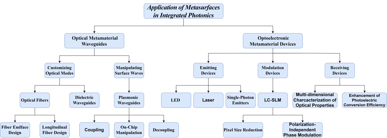
Figure 1: Structural dendrogram of this paper
2. Optical Metamaterial Waveguides
Metamaterial waveguides refer to a group of physical structures with engineered subwavelength features used to guide electromagnetic waves. Next, we will introduce recent research advancements in tailoring optical modes (in collaboration with dielectric waveguides and optical fibers) and manipulating surface waves (in collaboration with plasmonic waveguides). Table I lists the existing research related to optical metamaterial waveguides.
Table 1: Existing research on Optical Metamaterial Waveguides
Topic of the research | Year | Paper | Enhancements in this article |
Dielectric Waveguides | 2017 | [5] | Designed and demonstrated a phase-gradient metasurface structure based on gold nanorods on a Si3N4 waveguide |
2021 | [6] | Exploring optical neural networks by utilizing tunable gradient metasurface waveguide mode converters | |
2024 | [8] | Achieving full - color optical see - through (OST) with inverse - designed metasurface grating couplers | |
Optical Fibers (Fiber Endface Design) | 2019 | [9] | The conversion between the TM plane wave and the SPP mode is achieved by integrating a metasurface on the end face of a single-mode fiber. |
2023 | [10] | An electro-optic modulator of plasmonic meta-fiber based on the integration of the fiber end face has been designed. | |
2023 | [11] | By connecting multiple metasurfaces on the end face of the optical fiber, the output of the optical fiber is converted into different structured light fields. | |
2024 | [12] | High-quality optical skyrmions have been generated from meta-fibers. | |
Optical Fibers (Longitudinal Fiber Design) | 2019 | [13] | Guide the light rays to exceed the cutoff frequency, thereby enhancing the optical coupling and achieving low-latency communication. |
2021 | [14] | Achieve powerful dispersion control from ultraviolet and infrared to terahertz (THz) and microwave frequencies. | |
Plasmonic Waveguides (Coupling) | 2012 | [15] | Achieved perfect regulation with 100% efficiency for both propagating waves and surface waves. |
2017 | [16] | An efficient chiral modulating surface plasmon polariton coupler has been designed. | |
2017 | [17] | Design a single metasurface that has two arbitrary and independent phase distributions for the incident light of two orthogonal polarization states. | |
Plasmonic Waveguides (On-Chip Manipulation) | 2021 | [18] | Design and implement an on - chip metasurface for surface - wave optical rectification in visible light. |
2023 | [19] | A series of Pancharatnam-Berry (PB) metasurfaces operating in the microwave band were designed and fabricated to manipulate the wavefront of near-field surface waves. | |
Plasmonic Waveguides (Decoupling) | 2022 | [20] | Achieve more complex wavefront regulation of the far-field radiation of surface waves, such as focusing regulation, holographic regulation, and vortex beam regulation. |
2024 | [21] | Through the combined modulation of the diffraction phase, geometric phase, and propagation phase, the full-parameter modulation and directional multiplexing modulation of the equivalent Jones matrix are achieved. |
2.1. Customizing Optical Modes
In traditional waveguides without structural perturbations, mode conversion between two arbitrary electromagnetic modes is typically inaccessible due to wavevector mismatch. However, in metamaterial waveguides, metamaterial structures can provide effective momentum, enabling desired mode conversion.
Zhaoyi Li, Myoung-Hwan Kim, et al. designed and demonstrated a phase-gradient metasurface structure based on gold nanorods on a Si3N4 waveguide [5]. When the guided wave propagates in the direction opposite to the unidirectional phase gradient \( {k_{eff}}= \frac{dφ}{dx} \) of the gradient metasurface (generated by collective scattering effects), the total internal reflection angle decreases, corresponding to the conversion from a low-order waveguide mode to a high-order waveguide mode. Conversely, when light propagates in this direction, its wavevector \( {k_{mode}}= {n_{eff}}(Effective mode refractive index)×\frac{2π}{λ(Vacuum wavelength)} \) acquires an \( { k_{eff}} \) , resulting in the coupling from a high-order mode to a low-order mode. Should the fundamental mode propagating along this path be injected, it will couple to a surface wave and subsequently be absorbed by the plasmonic metasurface. However, light waves with opposite propagation directions can pass with lower loss while converting to higher-order modes. Using tunable gradient metasurface waveguide mode converters, optical neural networks can also be explored. Changming Wu, Seokhyeong Lee, et al. used Ge2Sb2Te5 (GST) phase-change material as a programmable metasurface waveguide mode converter, precisely controlling the conversion between two waveguide spatial modes (TE0 and TE1 modes) to encode weight parameters in matrix-vector multiplication calculations at 64 distinguishable levels [6]. A prototype optical convolutional neural network with a 2×2 array of GST converters was experimentally demonstrated to perform image processing and recognition between handwritten digits "1" and "2".
Forward-designed metamaterial waveguides possess a clear physical image, are relatively simple to design, and exhibit excellent performance. In contrast, inverse-designed metamaterial waveguides require substantial computational power during the implicit optimization process but can achieve complex functions difficult for forward design [7]. Manu Gopakumar, Gun-Yeal Lee, et al. developed a new AR display system combining a lensless holographic light engine with a metasurface waveguide optimized for full-color optical see-through (OST) AR display applications, featuring a compact design [8]. Compared to other waveguides, their optical system is unique in transmitting full-color 3D holographic images with high uniformity and transmission efficiency. This remarkable capability is attributed to the use of an inversely designed metasurface grating coupler. By optimizing the geometric structure of the metasurface grating using a rigorous coupled-wave analysis solver, the inverse-designed metasurface exhibits uniform transmittance regardless of the incident angle, demonstrating superior performance compared to traditional gratings.
The field of integrating metasurfaces at the end faces of optical fibers has shown immense potential in recent years. Hyun-Tae Kim and Miao Yu constructed a "lab-on-fiber" nanoprobe by designing a planar integrated distributed Bragg reflector on the end face of a single-mode fiber, capable of exciting two spatially separated high-Q resonance modes [9]. The design of the plasmonic crystal on the fiber leverages a thin 2D rectangular subwavelength Au grating, enabling the conversion between TM plane waves and SPP modes. Lei Zhang et al. demonstrated a plasmonic metamaterial fiber electro-optic modulator based on the integration of metamaterials at the end face of an optical fiber, achieving fast amplitude modulation [10]. The electro-optic modulator (EOM) consists of a three-layer structure, including a bottom layer of gold plasmonic metasurface, a middle layer of EO polymer, and a top layer of gold film. By adjusting the geometric parameters of the metasurface (such as the diameters and periods of nanodisks and nanoholes), the positions and quality factors of different optical modes can be quantitatively controlled. By connecting multiple metasurfaces on the end face of an optical fiber, the fiber output can also be converted into different structured light fields, including cylindrical vector beams, circularly polarized vortex beams, and arbitrary vector fields [11]. Optical skyrmions are an emerging class of structured light with complex particle-like topological structures and immense potential to revolutionize modern informatics. Tiantian He et al. successfully generated high-quality optical skyrmions from metafibers and verified their exceptional properties [12]. Compared to optical metamaterial tips, metamaterial fibers provide a broader stage for deploying metastructures, enabling the customization of fiber mode propagation and dispersion. However, they also impose higher quality control requirements on the subwavelength structures required along the entire fiber. For example, hollow-core fibers with hyperbolic metamaterial claddings can guide light beyond the cutoff frequency, enhancing optical coupling [13] and enabling low-latency communication. Metamaterial claddings, comprising diverse material combinations, facilitate robust dispersion control across a broad spectrum ranging from ultraviolet to infrared, and extending to terahertz (THz) and microwave frequencies. This approach effectively circumvents the structural and material characteristic limitations inherent in traditional silicon fibers [14].
2.2. Manipulating Surface Waves
The manipulation of surface waves via plasmonic metamaterial waveguides primarily entails three distinct processes: the coupling of propagating waves into surface waves, the on-chip manipulation of surface waves, and the decoupling of surface waves back into propagating waves. Subsequently, this research will delve into the applications of metamaterial devices within these three processes.
Plasmonic metamaterial waveguides offer significant advantages in terms of volume and coupling efficiency. In 2012, Sun et al. achieved perfect control of propagating waves and surface waves with 100% efficiency using a resonant phase-gradient metasurface [15]. Among them, the reflection phase is linearly distributed along the surface, with a linear phase gradient of \( \frac{dφ}{dx}=ξ \) , which is equivalent to the metasurface providing an additional wave vector \( ξ \) to the incident wave, thereby resolving the issue of horizontal wave vector mismatch. Compared to resonant phases, metasurfaces with geometric phases are easier to design and fabricate. In 2017, Duan designed a geometric phase-based surface plasmon polariton coupling metasurface [16]. This coupler consists of two parts: an excitation region for generating SPPs and an intrinsic metasurface region for guiding SPPs. By optimizing the polarization conversion efficiency of the metasurface units, near-100% excitation is achieved, and the intrinsic region can guide SPPs with both TE and TM polarizations and excite their propagation in the intrinsic region. The limitation of geometric phase metasurfaces lies in their applicability to circular polarization only. To overcome this limitation, Mueller et al. proposed a design method that combines propagation phases and geometric phases, enabling the design of a single metasurface with two arbitrary and independent phase distributions for incident light with two orthogonal polarization states (including linear, circular, and elliptical polarizations) [17].
Simultaneously, the rapid development of plasmonic metamaterial waveguides has opened new avenues for near-field manipulation. Rui Yang et al. designed and implemented an on-chip metasurface for optical directional rectification of visible light, achieving rectification of obliquely incident light through cascaded semi-elliptical and trapezoidal plasmonic nanowires [18]. The semi-elliptical structure focuses light to deep subwavelength scales, while the trapezoidal antenna imparts slightly different modulation phases to the surface waves, ultimately directing them in the same direction. The fabrication process of this on-chip metasurface is compatible with conventional nanomanufacturing techniques, facilitating easy integration into existing photonic systems. Weikang Pan, Zhuo Wang, et al. designed and fabricated a series of PB metasurfaces operating in the microwave range to manipulate the wavefronts of near-field surface waves [19]. They can deflect surface waves to predetermined angles over a broad frequency range with a deflection efficiency of up to 93%, while also achieving the generation of surface wave focusing and diffraction-free beams (such as Bessel beams and Airy beams), validating the complex wavefront shaping capability of metasurfaces. Compared to traditional methods, surface wave manipulation methods based on geometric phase metasurfaces offer advantages such as single-mode operation, high efficiency, ease of integration, and diverse functionalities. This surface wave manipulation method holds broad application prospects in on-chip integrated optics, such as on-chip switches, plasmonic tweezers, near-field imaging, and optical computing.
In many photonic applications, plasmonic metamaterial waveguides can decouple near-field surface waves into far-field plane waves. When encountering discontinuous interfaces (e.g., protrusions, holes, grooves), surface waves can partially scatter into free space, but the radiation intensity and direction are difficult to control. By designing PB metasurfaces with linear phase gradients, the conversion of surface waves into unidirectional propagating waves can be achieved. By adjusting the orientation angle distribution of the meta-units, the propagation direction of the propagating wave can be controlled. Compared to traditional diffractive optical devices and resonant metasurfaces, geometric phase metasurface devices exhibit advantages such as high efficiency, single-mode operation, ease of integration, and diverse functionalities. Furthermore, by further designing the orientation angle distribution of the meta-units, more complex wavefront manipulations of surface wave far-field radiation can be realized, such as focusing control, holographic control, and vortex beam control [20]. However, the number of controllable parameters in the equivalent Jones matrix of meta-units using only geometric phases is still limited, restricting the number of multiplexing channels. Jitao Ji et al. adopted a meta-unit cell design with four elements, achieving full-parameter modulation of the equivalent Jones matrix through combined modulation of diffractive phases and geometric phases. They further integrated propagation phases to realize directional multiplexing modulation of the Jones matrix [21]. The experiment successfully demonstrated four independent amplitude-phase channels, comprising two nanoprinted images and two holographic images. Through the introduction of a propagation matrix, eight holographic images corresponding to four distinct illumination directions were realized. This achievement paves a new avenue for high-capacity multiplexing of guided wave radiation and holds potential to drive advancements in photonic integrated technology.
3. Optoelectronic Metamaterial Devices
Here, this section focuses on recent remarkable advancements in metamaterials for emitters, receivers, and modulating devices. Table II lists the existing research related to optoelectronic metamaterial devices.
Table 2:Existing research on Optoelectronic Metamaterial Devices
Topic of the research | Year | Paper | Enhancements in this article |
Emitting Devices (LED) | 2025 | [22] | A GaN micro-resonant cavity light-emitting diode based on metasurface integration has been designed, which has achieved significant improvements in both the emission efficiency, deflection efficiency, and collection efficiency. |
Emitting Devices (Laser) | 2023 | [23] | On-chip generation and manipulation of vector beams on Vertical-Cavity Surface-Emitting Lasers (VCSELs) are achieved by using metasurfaces. |
2020 | [24] | The rapid tuning of the laser characteristics is achieved by breaking the symmetry of the BIC mode. | |
Emitting Devices (Single-Photon Emitters) | 2023 | [25] | Achieve multi-channel single-photon emission by using a metasurface designed based on scattering holography. |
2020 | [26] | Achieved flexible manipulation of the spin state and propagation direction of single-photon emission. | |
Receiving Devices (Measure a multitude of optical characteristics) | 2022 | [27] | Demonstrate a metasurface diffraction neural network based on multiplexing for on-chip multi-channel sensing within the visible light range. |
Receiving Devices (Enhance the photoelectric conversion efficiency) | 2022 | [28] | The perovskite metasurface photodetector prepared has achieved enhanced broadband absorption within the wavelength range of 300-800 nm. |
2022 | [29] | A planar wide-angle imaging camera based on a metalens array has been designed, achieving wide-angle imaging with an angle of more than 120°. | |
Modulation Devices (LC-SLM) | 2023 | [30] | A PI-LCoS-SLM device with a 4K resolution has been designed, and polarization-independent phase modulation has been successfully achieved in the target C+L telecommunication band. |
2022 | [31] | The metasurface-based LC-SLM designed achieves small pixel and multi-spectral operation. |
3.1. Emitting Devices
Integrating metasurfaces into LEDs can significantly improve emission and extraction efficiency, as well as enhance the angular and polarization characteristics of emitted light, based on the design. For instance, metasurfaces can be directly patterned onto the top or bottom surface (i.e., contact layer) of LED devices, serving as far-field wavefront transformers. Huamao Huang et al. designed a GaN microcavity light-emitting diode integrated with a metasurface, achieving substantial enhancements in emission efficiency, deflection efficiency, and collection efficiency [22].
Metasurface-based lasers enable precise control over emission characteristics. For example, vector beams can be generated and manipulated on-chip using metasurfaces on VCSELs, including multi-beam directional emission, vector holographic display, and vector vortex beams. This is significant for developing ultra-compact, lightweight, and scalable vector beam sources [23]. Simultaneously, metasurfaces enable rapid tuning of laser characteristics, crucial for applications requiring fast responses, such as optical switches and sensing technologies. BICs (Bound States in the Continuum) are special solutions to wave equations, manifesting as localized wave functions in radiation bands. They exhibit ultra-high Q-factors, low-threshold laser characteristics, and predicted vortex behavior carrying different topological charges. These properties make BICs highly attractive in active photonics, particularly for the design of vortex microlasers. Can Huang et al. used a 220-nm-thick lead bromide perovskite (MAPbBr3) film as the core material of the metasurface, with an array of square holes. At room temperature, using a frequency-doubled titanium sapphire laser to pump the perovskite metasurface, they successfully achieved vortex laser emission [24]. Metasurfaces are highly sensitive to symmetry-breaking perturbations. By altering the shape or configuration of the pump light (e.g., from circular to elliptical pump light, or using two overlapping circular pump lights), the symmetry of the BIC mode can be broken. This symmetry breaking leads to a switch between vortex beam and linearly polarized beam laser emission, with switching times reaching the picosecond scale, significantly faster than traditional microlasers. Additionally, due to the ultra-high Q-factor and low-threshold laser characteristics of the BIC mode, the vortex microlaser based on this metasurface consumes extremely low energy during laser emission.
Metasurface-based single-photon emitters can address the shortcomings of traditional devices in free space, including low spontaneous emission rates, broad emission spectra, and nearly omnidirectional emission directions. Danylo Komisar et al. proposed a method for achieving multi-channel single-photon emission using a metasurface designed with scattering holography. This method enables simultaneous control over the polarization and direction of single-photon emission in multiple predetermined directions through non-radiative coupling of quantum emitters (QEs) with surface plasmon polaritons (SPPs). The study demonstrated a highly compact, efficient, and versatile single-photon source integrating single-photon emission, collimation, and polarization beam-splitting functionalities [25]. Yanjun Bao et al. proposed a device that precisely integrates quantum dots with a spin-splitting bifocal metasurface (SSBM), enabling flexible manipulation of the spin state and propagation direction of single-photon emission. Compared to traditional single-photon sources, this device exhibits higher spontaneous emission rates, narrower emission spectra, and better directionality [26].
3.2. Receiving Devices
Traditional photoelectric receiving devices often lose all other information carried by incident photons except for light intensity during the photoelectric detection process. Therefore, it is quite difficult to directly detect other characteristics besides light intensity using traditional photoelectric detectors, and bulky optical devices are usually required. The emergence of metasurfaces provides a promising new platform for detecting these rich optical properties. For example, Xuhao Luo et al. demonstrated a multiplexed metasurface diffraction neural network (MDNN) integrated with a complementary metal-oxide-semiconductor (CMOS) imaging sensor for on-chip multichannel sensing in the visible light range [27]. The input signal, which carries information pertaining to the object to be recognized in the form of amplitude or phase, undergoes modulation by the metasurface. Consequently, the energy is redistributed to distinct detection areas, each corresponding to a specific recognition category. Furthermore, the CMOS sensor, integrated with the metasurface, is capable of distinguishing between 8 different images with high accuracy, thereby showcasing significant potential in the fields of computer vision processing and automotive camera image recognition. Furthermore, metasurfaces can also be used to improve the photoelectric conversion efficiency of traditional photoelectric receiving devices and achieve efficient, broadband absorption by optimizing the unit structure, arrangement, and material selection of metamaterials. For example, J. He et al. designed a metasurface composed of perovskite nanodisk arrays, which achieved broadband absorption enhancement in the wavelength range of 300-800 nm by optimizing the diameter, height, and period of the nanodisks [28]. Compared with other planar photoelectric detectors, the perovskite metasurface photodetector they prepared performs excellently in terms of active layer thickness, spectral range, response speed, and photoelectric conversion efficiency. By integrating metasurfaces, the detection angle of receiving devices has been steadily improved. Ji Chen et al. designed a planar wide-angle imaging camera based on a metal lens array, which achieves wide-angle imaging of more than 120° while maintaining high imaging quality through a carefully designed metal lens array [29].
3.3. Modulation Devices
Since the introduction of liquid crystal on silicon (LCoS) spatial light modulators (SLMs), a notable limitation has been identified: these devices are capable of phase-modulating only linearly polarized light whose polarization direction is aligned with the orientation of the liquid crystal molecules. Conversely, they exhibit minimal effect on linearly polarized light oriented in the orthogonal direction. Therefore, Zhaoxiang Zhu et al. designed a PI-LCoS-SLM device with 4K resolution [30]. By embedding a carefully designed metasurface between the original 4K LCoS backplane and the liquid crystal layer, they successfully achieved polarization-independent phase modulation in the target C+L telecommunication bands. Based on this device, they also demonstrated typical application functions including polarization-independent beam steering and holographic imaging, and as expected, the polarization-dependent loss was low (<0.3dB), while other performance metrics of interest (e.g., total efficiency >40% for beam steering angles up to 4°) were comparable to current commercial polarization-dependent LCoS devices.
LCoS SLMs also have limitations in terms of the minimum pixel size. Currently, the minimum pixel size of commercial one-dimensional (1D) reflective silicon-based LCoS SLMs is 1.6, while the minimum pixel size of commercial two-dimensional (2D) reflective LCoS devices is still over 3, a limit that has hardly been broken in the past decade. Active tunable metasurfaces can effectively address this issue. Mansha et al. proposed a novel design that allows metasurface-based LC-SLMs to achieve small pixels and multispectral operation [31]. Their design is based on liquid crystal-tunable Fabry-Perot nanocavities, featuring (i) thin (sub-micrometer) liquid crystal cells to improve response time and reduce cross-talk between pixels, (ii) small (1) pixels to achieve a wide field of view (18°), and (iii) the ability to operate simultaneously at multiple wavelengths, including red (R), green (G), and blue (B) wavelengths in the visible spectrum. This device, known as a Fabry-Perot spatial light modulator (FP-SLM), can achieve high reflectivity and large phase modulation simultaneously at these multiple wavelengths.
4. Conclusion
Metasurfaces, as a revolutionary platform for manipulating electromagnetic waves, hold immense potential in advancing integrated photonics. However, their practical implementation faces significant challenges across design, manufacturing, and integration. Traditional forward design methods, while mature, struggle to address the growing demands for multifunctional, broadband, and high-density devices due to their reliance on empirical adjustments and limited exploration of complex structural spaces. Inverse design, driven by optimization algorithms and computational advancements, offers a promising alternative by systematically navigating vast design spaces to achieve optimal performance. Nevertheless, critical questions regarding solution existence, computational boundaries, and the development of fully automated design tools remain unresolved.
Manufacturing metasurfaces with subwavelength precision necessitates innovations in materials and processes. Nanoimprinting and CMOS-compatible techniques show potential for scalable production, yet challenges in structural stability, material compatibility (e.g., plasmonic loss mitigation), and cost-effective fabrication persist. Furthermore, integrating metasurfaces into photonic circuits requires harmonizing diverse platforms—such as silicon photonics and thin-film lithium niobate—while addressing the inherent limitations of monolithic systems. Hybrid integration strategies, leveraging heterogeneous materials (e.g., III-V semiconductors for lasers), exemplify a pragmatic pathway toward functional photonic systems.
Looking ahead, metasurfaces are poised to become indispensable in integrated photonics. The integration of artificial intelligence with inverse design is anticipated to expedite the identification of innovative structures and functionalities. Concurrently, interdisciplinary collaboration between academic institutions and industry sectors will effectively bridge the divide between laboratory-based innovations and their commercial realization. By addressing existing challenges, metasurface-based devices could revolutionize fields ranging from high-speed data communication and biomedical sensing to quantum computing. Ultimately, the synergy of advanced design methodologies, material science breakthroughs, and scalable manufacturing will unlock the full potential of metasurfaces, ushering in a new era of compact, multifunctional photonic systems.
References
[1]. Lifante, G. (2003). Integrated photonics: fundamentals. John Wiley & Sons.
[2]. Cui, T. J., Smith, D. R., & Liu, R. (2010). Metamaterials (p. 1). New York: springer.
[3]. Choy, T. C. (2015). Effective medium theory: principles and applications (Vol. 165). Oxford University Press.
[4]. Sun, L., Zhang, Y., He, Y., Wang, H. & Su, Y. (2020). Subwavelength structured silicon waveguides and photonic devices. Nanophotonics, 9(6), 1321-1340. https://doi.org/10.1515/nanoph-2020-0070
[5]. Li, Z., Kim, MH., Wang, C. et al. Controlling propagation and coupling of waveguide modes using phase-gradient metasurfaces. Nature Nanotech 12, 675–683 (2017).
[6]. Wu, C. M. et al. Programmable phase-change metasurfaces on waveguides for multimode photonic convolutional neural network. Nat. Commun. 12, 96(2021).
[7]. Estakhri, N. M., Edwards, B. & Engheta, N. Inverse-designed metastructures that solve equations. Science 363, 1333–1338 (2019).
[8]. Gopakumar, M., Lee, GY., Choi, S. et al. Full-colour 3D holographic augmented-reality displays with metasurface waveguides. Nature 629, 791–797 (2024).
[9]. Kim, HT., Yu, M. Lab-on-Fiber Nanoprobe with Dual High-Q Rayleigh Anomaly-Surface Plasmon Polariton Resonances for Multiparameter Sensing. Sci Rep 9, 1922 (2019).
[10]. Zhang, L., Sun, X., Yu, H. et al. Plasmonic metafibers electro-optic modulators. Light Sci Appl 12, 198 (2023).
[11]. Li, C., Wieduwilt, T., Wendisch, F.J. et al. Metafiber transforming arbitrarily structured light. Nat Commun 14, 7222 (2023).
[12]. He, T., Meng, Y., Wang, L. et al. Optical skyrmions from metafibers with subwavelength features. Nat Commun 15, 10141 (2024).
[13]. Bhardwaj, A., Srivastava, K. V. & Ramakrishna, S. A. Enhanced coupling of light from subwavelength sources into a hyperbolic metamaterial fiber. J. Lightwave Technol. 37, 3064–3072 (2019).
[14]. Meng, Y., Chen, Y., Lu, L. et al. Optical meta-waveguides for integrated photonics and beyond. Light Sci Appl 10, 235 (2021).
[15]. Sun, S. L. et al. Gradient-indexmeta-surfaces as a bridge linking propagating waves and surface waves. Nat. Mater. 11, 426–431 (2012).
[16]. Duan, J. W. et al. High-efficiency chirality-modulated spoof surface plasmon meta-coupler. Sci. Rep. 7, 1354 (2017)
[17]. Mueller, J. P. B. et al. Metasurface polarization optics: Independent phase control of arbitrary orthogonal states of polarization. Phys. Rev. Lett. 118,113901 (2017).
[18]. R. Yang, Y. Shi, S. Wan, Z. Wang and Z. Li, "On-Chip Metasurface for Optical Directional Rectification," in Journal of Lightwave Technology, vol. 39, no. 17, pp. 5558-5562, 1 Sept.1, 2021
[19]. Pan, W., Wang, Z., Chen, Y., Zheng, X., Li, S., Tian, X., ... & Sun, S. (2023). Efficiently controlling near-field wavefronts via designer metasurfaces. ACS Photonics, 10(7), 2423-2431.
[20]. Pan, W., Wang, Z., Chen, Y., Li, S., Zheng, X., Tian, X., Chen, C., Xu, N., He, Q., Zhou, L. & Sun, S. (2022). High-efficiency generation of far-field spin-polarized wavefronts via designer surface wave metasurfaces. Nanophotonics, 11(9), 2025-2036.
[21]. Ji, J., Li, J., Wang, Z. et al. On-chip multifunctional metasurfaces with full-parametric multiplexed Jones matrix. Nat Commun 15, 8271 (2024)
[22]. Huang, H., Zeng, H., Zhang, J., & Liang, J. (2025). Efficient polarization emission from metasurface-integrated resonant cavity light-emitting diodes. Journal of Physics D: Applied Physics.
[23]. Fu, P., Ni, P. N., Wu, B., Pei, X. Z., Wang, Q. H., Chen, P. P., ... & Xie, Y. Y. (2023). Metasurface enabled on‐chip generation and manipulation of vector beams from vertical cavity surface‐emitting lasers. Advanced Materials, 35(12), 2204286.
[24]. Huang, C., Zhang, C., Xiao, S., Wang, Y., Fan, Y., Liu, Y., ... & Song, Q. (2020). Ultrafast control of vortex microlasers. Science, 367(6481), 1018-1021.
[25]. Komisar, D., Kumar, S., Kan, Y., Meng, C., Kulikova, L. F., Davydov, V. A., ... & Bozhevolnyi, S. I. (2023). Multiple channelling single-photon emission with scattering holography designed metasurfaces. Nature Communications, 14(1), 6253.
[26]. Bao, Y., Lin, Q., Su, R., Zhou, Z. K., Song, J., Li, J., & Wang, X. H. (2020). On-demand spin-state manipulation of single-photon emission from quantum dot integrated with metasurface. Science advances, 6(31), eaba8761.
[27]. Luo, X., Hu, Y., Ou, X. et al. Metasurface-enabled on-chip multiplexed diffractive neural networks in the visible. Light Sci Appl 11, 158 (2022).
[28]. He, J., Li, C. Y., Qi, D. X., Cai, Q., Liu, Y., Fan, R. H., ... & Wang, M. (2022). Improving photoelectric conversion with broadband perovskite metasurface. Nano Letters, 22(16), 6655-6663.
[29]. Chen, J., Ye, X., Gao, S., Chen, Y., Zhao, Y., Huang, C., ... & Li, T. (2022). Planar wide-angle-imaging camera enabled by metalens array. Optica, 9(4), 431-437.
[30]. Zhu, Z., Wen, Y., Li, J.et al.Metasurface-enabled polarization-independent LCoS spatial light modulator for 4K resolution and beyond.Light Sci Appl 12, 151 (2023).
[31]. Mansha, S., Moitra, P., Xu, X. et al. High resolution multispectral spatial light modulators based on tunable Fabry-Perot nanocavities. Light Sci Appl 11, 141 (2022).
Cite this article
Zhou,W. (2025). Application of Metasurfaces in Integrated Photonics. Applied and Computational Engineering,149,35-44.
Data availability
The datasets used and/or analyzed during the current study will be available from the authors upon reasonable request.
Disclaimer/Publisher's Note
The statements, opinions and data contained in all publications are solely those of the individual author(s) and contributor(s) and not of EWA Publishing and/or the editor(s). EWA Publishing and/or the editor(s) disclaim responsibility for any injury to people or property resulting from any ideas, methods, instructions or products referred to in the content.
About volume
Volume title: Proceedings of CONF-MSS 2025 Symposium: Automation and Smart Technologies in Petroleum Engineering
© 2024 by the author(s). Licensee EWA Publishing, Oxford, UK. This article is an open access article distributed under the terms and
conditions of the Creative Commons Attribution (CC BY) license. Authors who
publish this series agree to the following terms:
1. Authors retain copyright and grant the series right of first publication with the work simultaneously licensed under a Creative Commons
Attribution License that allows others to share the work with an acknowledgment of the work's authorship and initial publication in this
series.
2. Authors are able to enter into separate, additional contractual arrangements for the non-exclusive distribution of the series's published
version of the work (e.g., post it to an institutional repository or publish it in a book), with an acknowledgment of its initial
publication in this series.
3. Authors are permitted and encouraged to post their work online (e.g., in institutional repositories or on their website) prior to and
during the submission process, as it can lead to productive exchanges, as well as earlier and greater citation of published work (See
Open access policy for details).
References
[1]. Lifante, G. (2003). Integrated photonics: fundamentals. John Wiley & Sons.
[2]. Cui, T. J., Smith, D. R., & Liu, R. (2010). Metamaterials (p. 1). New York: springer.
[3]. Choy, T. C. (2015). Effective medium theory: principles and applications (Vol. 165). Oxford University Press.
[4]. Sun, L., Zhang, Y., He, Y., Wang, H. & Su, Y. (2020). Subwavelength structured silicon waveguides and photonic devices. Nanophotonics, 9(6), 1321-1340. https://doi.org/10.1515/nanoph-2020-0070
[5]. Li, Z., Kim, MH., Wang, C. et al. Controlling propagation and coupling of waveguide modes using phase-gradient metasurfaces. Nature Nanotech 12, 675–683 (2017).
[6]. Wu, C. M. et al. Programmable phase-change metasurfaces on waveguides for multimode photonic convolutional neural network. Nat. Commun. 12, 96(2021).
[7]. Estakhri, N. M., Edwards, B. & Engheta, N. Inverse-designed metastructures that solve equations. Science 363, 1333–1338 (2019).
[8]. Gopakumar, M., Lee, GY., Choi, S. et al. Full-colour 3D holographic augmented-reality displays with metasurface waveguides. Nature 629, 791–797 (2024).
[9]. Kim, HT., Yu, M. Lab-on-Fiber Nanoprobe with Dual High-Q Rayleigh Anomaly-Surface Plasmon Polariton Resonances for Multiparameter Sensing. Sci Rep 9, 1922 (2019).
[10]. Zhang, L., Sun, X., Yu, H. et al. Plasmonic metafibers electro-optic modulators. Light Sci Appl 12, 198 (2023).
[11]. Li, C., Wieduwilt, T., Wendisch, F.J. et al. Metafiber transforming arbitrarily structured light. Nat Commun 14, 7222 (2023).
[12]. He, T., Meng, Y., Wang, L. et al. Optical skyrmions from metafibers with subwavelength features. Nat Commun 15, 10141 (2024).
[13]. Bhardwaj, A., Srivastava, K. V. & Ramakrishna, S. A. Enhanced coupling of light from subwavelength sources into a hyperbolic metamaterial fiber. J. Lightwave Technol. 37, 3064–3072 (2019).
[14]. Meng, Y., Chen, Y., Lu, L. et al. Optical meta-waveguides for integrated photonics and beyond. Light Sci Appl 10, 235 (2021).
[15]. Sun, S. L. et al. Gradient-indexmeta-surfaces as a bridge linking propagating waves and surface waves. Nat. Mater. 11, 426–431 (2012).
[16]. Duan, J. W. et al. High-efficiency chirality-modulated spoof surface plasmon meta-coupler. Sci. Rep. 7, 1354 (2017)
[17]. Mueller, J. P. B. et al. Metasurface polarization optics: Independent phase control of arbitrary orthogonal states of polarization. Phys. Rev. Lett. 118,113901 (2017).
[18]. R. Yang, Y. Shi, S. Wan, Z. Wang and Z. Li, "On-Chip Metasurface for Optical Directional Rectification," in Journal of Lightwave Technology, vol. 39, no. 17, pp. 5558-5562, 1 Sept.1, 2021
[19]. Pan, W., Wang, Z., Chen, Y., Zheng, X., Li, S., Tian, X., ... & Sun, S. (2023). Efficiently controlling near-field wavefronts via designer metasurfaces. ACS Photonics, 10(7), 2423-2431.
[20]. Pan, W., Wang, Z., Chen, Y., Li, S., Zheng, X., Tian, X., Chen, C., Xu, N., He, Q., Zhou, L. & Sun, S. (2022). High-efficiency generation of far-field spin-polarized wavefronts via designer surface wave metasurfaces. Nanophotonics, 11(9), 2025-2036.
[21]. Ji, J., Li, J., Wang, Z. et al. On-chip multifunctional metasurfaces with full-parametric multiplexed Jones matrix. Nat Commun 15, 8271 (2024)
[22]. Huang, H., Zeng, H., Zhang, J., & Liang, J. (2025). Efficient polarization emission from metasurface-integrated resonant cavity light-emitting diodes. Journal of Physics D: Applied Physics.
[23]. Fu, P., Ni, P. N., Wu, B., Pei, X. Z., Wang, Q. H., Chen, P. P., ... & Xie, Y. Y. (2023). Metasurface enabled on‐chip generation and manipulation of vector beams from vertical cavity surface‐emitting lasers. Advanced Materials, 35(12), 2204286.
[24]. Huang, C., Zhang, C., Xiao, S., Wang, Y., Fan, Y., Liu, Y., ... & Song, Q. (2020). Ultrafast control of vortex microlasers. Science, 367(6481), 1018-1021.
[25]. Komisar, D., Kumar, S., Kan, Y., Meng, C., Kulikova, L. F., Davydov, V. A., ... & Bozhevolnyi, S. I. (2023). Multiple channelling single-photon emission with scattering holography designed metasurfaces. Nature Communications, 14(1), 6253.
[26]. Bao, Y., Lin, Q., Su, R., Zhou, Z. K., Song, J., Li, J., & Wang, X. H. (2020). On-demand spin-state manipulation of single-photon emission from quantum dot integrated with metasurface. Science advances, 6(31), eaba8761.
[27]. Luo, X., Hu, Y., Ou, X. et al. Metasurface-enabled on-chip multiplexed diffractive neural networks in the visible. Light Sci Appl 11, 158 (2022).
[28]. He, J., Li, C. Y., Qi, D. X., Cai, Q., Liu, Y., Fan, R. H., ... & Wang, M. (2022). Improving photoelectric conversion with broadband perovskite metasurface. Nano Letters, 22(16), 6655-6663.
[29]. Chen, J., Ye, X., Gao, S., Chen, Y., Zhao, Y., Huang, C., ... & Li, T. (2022). Planar wide-angle-imaging camera enabled by metalens array. Optica, 9(4), 431-437.
[30]. Zhu, Z., Wen, Y., Li, J.et al.Metasurface-enabled polarization-independent LCoS spatial light modulator for 4K resolution and beyond.Light Sci Appl 12, 151 (2023).
[31]. Mansha, S., Moitra, P., Xu, X. et al. High resolution multispectral spatial light modulators based on tunable Fabry-Perot nanocavities. Light Sci Appl 11, 141 (2022).