1. Introduction
In modern applications such as wireless communication, satellite navigation, and precision measurement, the ring oscillator—serving as the core component of frequency sources—plays a critical role in determining signal integrity, communication range, and positioning accuracy. Traditional quartz crystal oscillators (e.g., quartz VCXOs) have dominated the mainstream market due to their excellent frequency stability. However, their high cost, large size, and limited tuning range fail to meet the emerging requirements of Internet of Things (IoT) devices and miniaturized radar modules. In recent years, dielectric resonator oscillators (DROs) and integrated phase-locked loop (PLL) technologies have made progress in terms of miniaturization and cost reduction. Nevertheless, in frequency bands above 10 GHz, their phase noise performance still generally falls short of -100 dBc/Hz@1 kHz. Additionally, these technologies suffer from challenges such as temperature sensitivity and process variation.
Multistage ring oscillators based on inverters offer significant advantages in terms of high performance and low cost. By tuning key electrical parameters—such as the output current, output impedance, and the number of cascaded inverter stages—precise, low-noise frequency output can be achieved under specific voltage conditions. Optimized electrical characteristics not only improve the oscillator's noise performance and frequency stability but also enhance its adaptability to temperature-sensitive components and its applicability in constructing high-precision encrypted communication networks. In recent years, ring oscillators have attracted considerable academic attention. In [1], the phase noise was reduced to -113.1 dBc/Hz by increasing the number of delay stages, achieving a 7 dB improvement at the cost of increased power consumption, which rose to 100.3 mW without optimization. In [2], the switching speed of the oscillator’s delay unit was enhanced by adding MOS transistors and incorporating a positive feedback structure, resulting in a frequency increase of up to 300%. In [3], a five-stage ring oscillator model was developed to analyze phase noise and power consumption, followed by transistor sizing optimization. The resulting VCO achieved a phase noise of -111 dBc/Hz at 1 MHz offset from a 400 MHz center frequency, with power consumption of only 158 μW. Reference [4], utilizing the 65nm CMOS process, reduced total channel thermal noise injected into the VCO output node during output voltage transitions. At 645 MHz, it achieved a phase noise of -110.8 dBc/Hz at 1 MHz offset, with a power consumption of 10 mW under a 1-V supply. In [5], a VCO fabricated using a 0.35 μm CMOS process and composed of five delay units plus an output buffer demonstrated improved phase noise performance and linear tuning characteristics. The proposed VCO-based PLL sensor interface achieved a signal-to-noise ratio (SNR) of 88.4 dB over a 1 kHz bandwidth.
2. Circuit design
The schematic of a conventional ring oscillator based on inverter amplifiers is shown in Figure 1(a), while the schematic of a single inverter amplifier is illustrated in Figure 1(b). Five inverter amplifiers are connected in a closed loop to form an oscillation ring. The oscillation frequency of the loop is determined by the propagation delay of the ring; the frequency is inversely proportional to the total delay. Therefore, increasing the delay of the inverters leads to a reduction in oscillation frequency, and vice versa. Generally, there are two methods to increase the overall delay of the loop. The first is to increase the number of cascaded inverter stages, thereby increasing the total delay. However, this approach is not suitable when chip area and power consumption are constrained. The second method is to increase the delay of each individual inverter stage, which effectively increases the total loop delay without significantly impacting area or power. As shown in Figure 1(b), the inverter consists of a PMOS and an NMOS transistor connected in series. The gates of both transistors serve as the input terminal, while the drains are connected to form the output terminal. The W/L ratios of the PMOS and NMOS transistors are carefully designed to ensure that the output impedances of both transistors are matched.

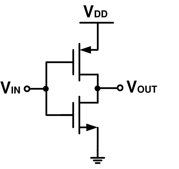
Figure 1: (a) Fifth-order ring voltage-controlled oscillator; (b) conventional inverter amplifier
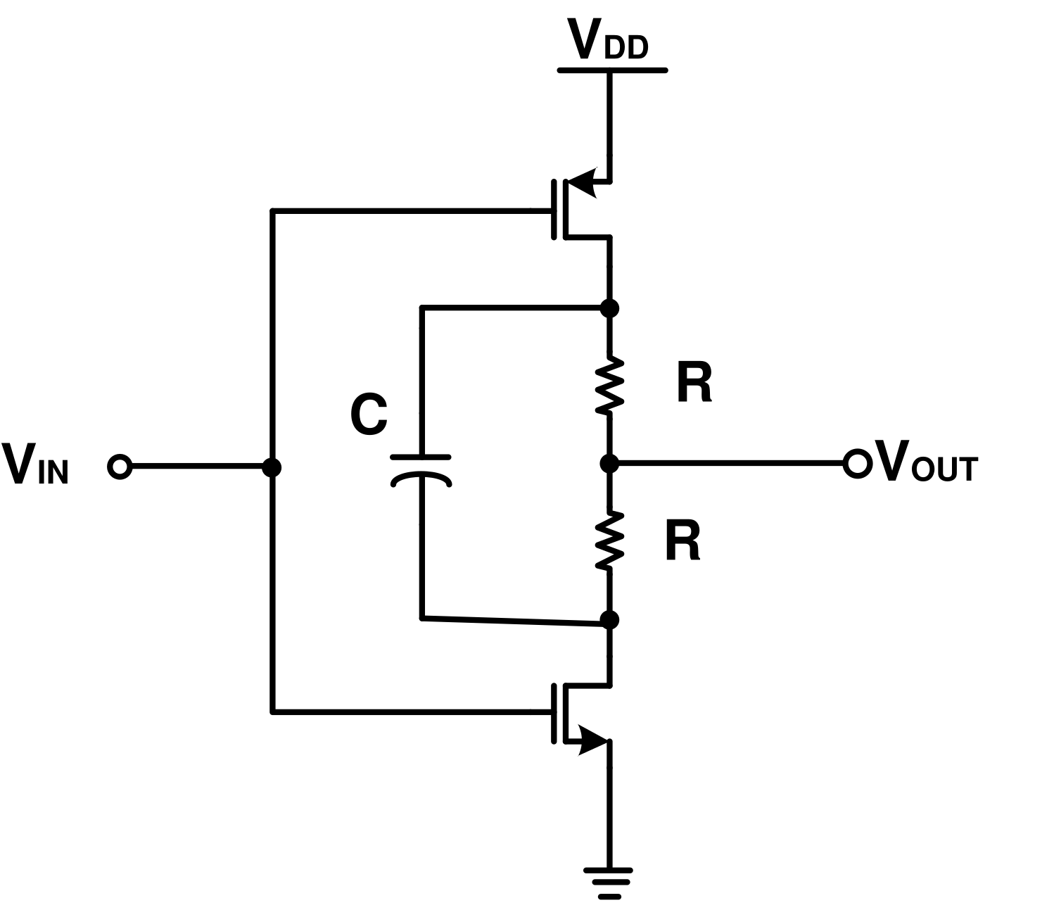
The proposed low-noise inverter amplifier is shown in Figure 2. A parallel RC network, consisting of a resistor R and a capacitor C, is inserted between the PMOS and NMOS transistors. On one hand, this RC network functions as a first-order low-pass filter, which effectively reduces the noise generated by the inverter amplifier. The output noise of a first-order low-pass filter formed by R and C is given by kT/C, where k is Boltzmann’s constant and T is the absolute temperature in Kelvin. Therefore, the thermal noise introduced by the resistor R is negligible. On the other hand, the resistor R increases the output impedance of the inverter amplifier, thereby enhancing the robustness of the ring oscillator without contributing to additional power consumption. As a result, replacing the traditional inverter amplifier with the proposed low-noise design as the delay cell in the voltage-controlled ring oscillator can further improve the oscillator’s overall performance.
3. Simulation results
The proposed low-phase-noise ring oscillator was simulated using the Cadence Virtuoso platform based on the TSMC 65nm CMOS RF process. The simulation results are shown in Figure 3~5.
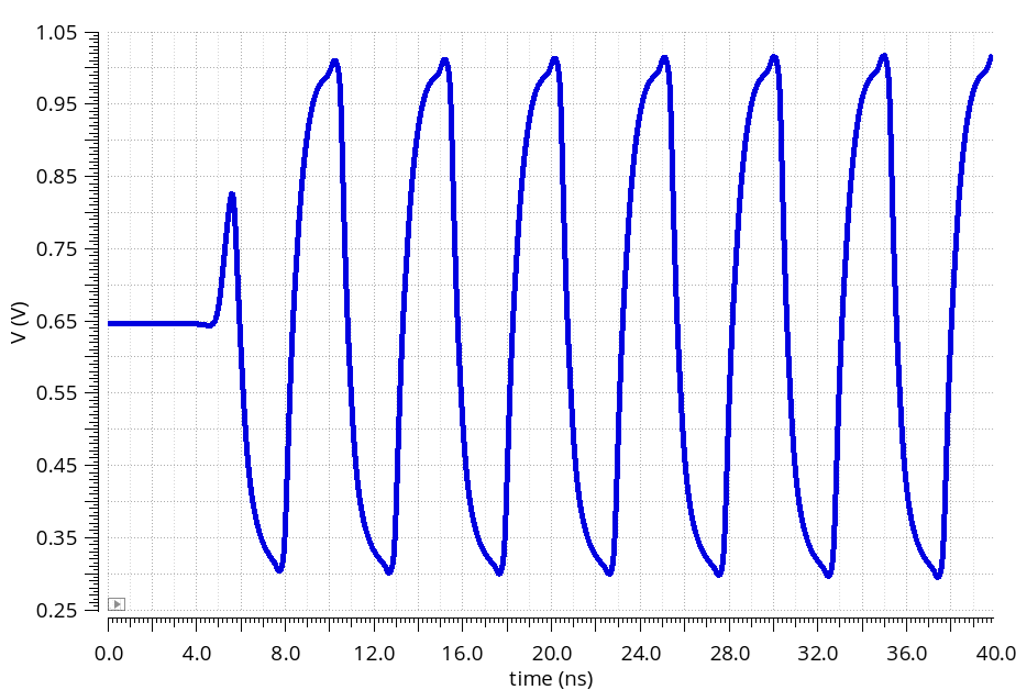
The oscillation waveform of the proposed oscillator circuit is shown in Figure 3. The startup time of the oscillation is approximately 10ns, and the peak-to-peak voltage of the waveform is about 700mVpp.
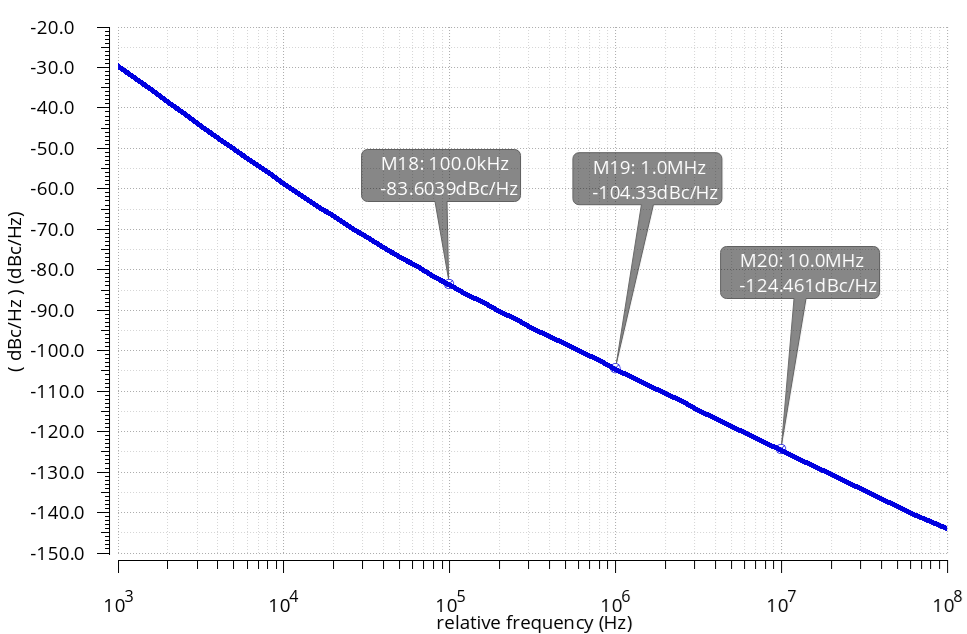
The simulated phase noise performance of the proposed oscillator circuit is shown in Figure 4. The phase noise is -83.6 dBc/Hz at a 100 kHz offset, -104.3 dBc/Hz at a 1 MHz offset, and -124.5 dBc/Hz at a 10 MHz offset.
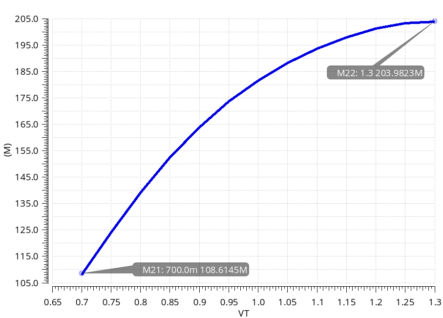
The simulated frequency tuning range of the proposed oscillator circuit under a control voltage varying from 0.7 V to 1.3 V is shown in Figure 5. The tunable frequency range extends from 108 MHz to 203 MHz.
4. Conclusion
Based on the TSMC 65nm CMOS RF process, a low-phase-noise fifth-order ring voltage-controlled oscillator (VCO) based on inverter circuits was designed. By adding two delay cells to the conventional three-stage inverter amplifier structure, the oscillation frequency of the loop was increased. Additionally, a parallel RC network was introduced between the PMOS and NMOS transistors, which effectively reduced the noise of the inverter amplifier. This design also enhanced the robustness of the ring oscillator by increasing the output impedance without incurring additional power consumption, thereby addressing the high power consumption issue of traditional amplifiers. Simulation results demonstrate that under a control voltage range of 0.7 V to 1.3 V, the proposed fifth-order ring VCO achieves a tunable frequency range from 108 MHz to 203 MHz. The phase noise performance is -83.6 dBc/Hz at a 100 kHz offset, -104.3 dBc/Hz at a 1 MHz offset, and -124.5 dBc/Hz at a 10 MHz offset. Compared to traditional ring oscillators, the proposed design exhibits improved phase noise performance with a typical power consumption of 30.3 μW, indicating promising application potential.
References
[1]. Abd Ghani, A. A., & Saparon, A. (2007, December 11–12). A 1.4 GHz CMOS low-phase noise voltage-controlled ring oscillator. In Proceedings of the 5th Student Conference on Research and Development (SCOReD 2007), Malaysia.
[2]. Suman, S., Bhardwaj, M., & Singh, B. P. (2012). An improved performance ring oscillator design. In Proceedings of the 2012 Second International Conference on Advanced Computing & Communication Technologies.
[3]. Ghafari, B., Koushaeian, L., Goodarzy, F., Evans, R., & Skafidas, E. (2013). An ultra-low-power and low-noise voltage-controlled ring oscillator for biomedical applications. In Proceedings of IEEE TENCON - Spring 2013.
[4]. Kim, J.-M., Kim, S., Lee, I.-Y., Han, S.-K., & Lee, S.-G. (2013). A low-noise four-stage voltage-controlled ring oscillator in deep-submicrometer CMOS technology. IEEE Transactions on Circuits and Systems II: Express Briefs, 60(2), 85–89.
[5]. Esmaeilzadeh, M., Audet, Y., Ali, M., & Sawa, M. (2022). A low-phase-noise CMOS ring voltage-controlled oscillator intended for time-based sensor interfaces. IEEE Access, 10, 101186–101197.
Cite this article
Wang,S. (2025). A Simulated Design of a Ring Oscillator with Phase Noise of -104.3 dBc/Hz@1MHz. Applied and Computational Engineering,161,41-46.
Data availability
The datasets used and/or analyzed during the current study will be available from the authors upon reasonable request.
Disclaimer/Publisher's Note
The statements, opinions and data contained in all publications are solely those of the individual author(s) and contributor(s) and not of EWA Publishing and/or the editor(s). EWA Publishing and/or the editor(s) disclaim responsibility for any injury to people or property resulting from any ideas, methods, instructions or products referred to in the content.
About volume
Volume title: Proceedings of the 3rd International Conference on Mechatronics and Smart Systems
© 2024 by the author(s). Licensee EWA Publishing, Oxford, UK. This article is an open access article distributed under the terms and
conditions of the Creative Commons Attribution (CC BY) license. Authors who
publish this series agree to the following terms:
1. Authors retain copyright and grant the series right of first publication with the work simultaneously licensed under a Creative Commons
Attribution License that allows others to share the work with an acknowledgment of the work's authorship and initial publication in this
series.
2. Authors are able to enter into separate, additional contractual arrangements for the non-exclusive distribution of the series's published
version of the work (e.g., post it to an institutional repository or publish it in a book), with an acknowledgment of its initial
publication in this series.
3. Authors are permitted and encouraged to post their work online (e.g., in institutional repositories or on their website) prior to and
during the submission process, as it can lead to productive exchanges, as well as earlier and greater citation of published work (See
Open access policy for details).
References
[1]. Abd Ghani, A. A., & Saparon, A. (2007, December 11–12). A 1.4 GHz CMOS low-phase noise voltage-controlled ring oscillator. In Proceedings of the 5th Student Conference on Research and Development (SCOReD 2007), Malaysia.
[2]. Suman, S., Bhardwaj, M., & Singh, B. P. (2012). An improved performance ring oscillator design. In Proceedings of the 2012 Second International Conference on Advanced Computing & Communication Technologies.
[3]. Ghafari, B., Koushaeian, L., Goodarzy, F., Evans, R., & Skafidas, E. (2013). An ultra-low-power and low-noise voltage-controlled ring oscillator for biomedical applications. In Proceedings of IEEE TENCON - Spring 2013.
[4]. Kim, J.-M., Kim, S., Lee, I.-Y., Han, S.-K., & Lee, S.-G. (2013). A low-noise four-stage voltage-controlled ring oscillator in deep-submicrometer CMOS technology. IEEE Transactions on Circuits and Systems II: Express Briefs, 60(2), 85–89.
[5]. Esmaeilzadeh, M., Audet, Y., Ali, M., & Sawa, M. (2022). A low-phase-noise CMOS ring voltage-controlled oscillator intended for time-based sensor interfaces. IEEE Access, 10, 101186–101197.


