


1. Introduction
GaN is a very important semiconductor material from Group III-V compounds. It usually appears in two types of crystal structures: wurtzite and zincblende, but the wurtzite one is more common. GaN is a typical example of a semiconductor with a wide bandgap. At room temperature, its bandgap is 3.4 eV, which is much wider than other common semiconductors like silicon (1.1 eV) and gallium arsenide (1.42 eV) [1,2]. Because of its wide bandgap, GaN has strong properties, like being able to handle high voltages (3 MV/cm), having good thermal conductivity, and letting electrons move in it quickly. GaN’s maximum hole energy and minimum electron energy are both at one spot (called the Γ point) of the Brillouin zone, which makes it a direct bandgap semiconductor. This key feature lets electron and hole pairs come together and make light easily, so GaN is great for making things like blue and UV LEDs and laser diodes. Furthermore, GaN can be mixed with aluminum nitride and indium nitride to make ternary alloys (AlGaN and InGaN), which allows their bandgap to change from 1.9 eV to 6.2 eV without any breaks. This gives designers a lot of freedom to make and improve their products. People are now very interested in using GaN in strong solid-state radio frequency (RF) uses. This technology might be very helpful for things like RF switches, high-power amplifiers (HPAs), and low-noise amplifiers (LNAs) [3]. This is mainly because GaN’s material properties are better than those of other semiconductors, like gallium arsenide (GaAs). Compared to GaAs, GaN has greater resistance to radiation and conducts heat better. GaN can also work at much higher temperatures, meaning its operation powers can be increased.
GaN is a leader among new-generation semiconductor materials and has changed optoelectronic devices. It has a direct bandgap of 3.4 eV that can be used for short-wavelength lighting. The structure design of InGaN/GaN multiple quantum wells can tune the emission wavelength to achieve efficient short-wavelength light emitters from ultraviolet (200 nm) to green light (520 nm). Blue single-chip LEDs based on GaN have modern quantum efficiencies above 80%, and this has greatly advanced the solid-state lighting revolution. The AlGaN material system in ultraviolet optoelectronic devices enables emission in the deep ultraviolet range (200 nm-365 nm). It has a unique and innovative edge that makes it difficult to replace in unique applications like UV curing and sterilization. GaN has good performance at high frequencies, and detectors that can reach GHz reaction times have been developed, making it highly promising in optical communication applications. Due to GaN’s wide band gap, the devices can be used in harsh environments such as high temperatures and strong radiation. Applications are also audio the military and aerospace. III-nitride semiconductors that can be used to create LEDs and laser diodes (LDs) have optical characteristics frequently used for solid-state lighting. A broad spectrum of direct bandgap energies can be covered by alloys of GaN (3.4 eV) and InN (0.7 eV), which are frequently used [4].
GaN is a great material for a semiconductor laser due to its unique optoelectronic properties. From the optoelectronic properties aspect, GaN has a direct bandgap of 3.4 eV. This indicates that the lowest point of the conduction band and the highest point in the valence band coincide at the Γ point in the Brillouin zone. The emission wavelength can be tuned from the near-ultraviolet (365 nm) to green light (530 nm) by varying the alloy composition of InGaN ternary alloys. GaN also has a high optical gain coefficient (103cm-1) as well as a high refractive index (n~2.4).
Three key advantages of GaN-based materials can be used in semi-lasers. Blue laser diodes: Commercial InGaN/GaN multiple quantum well (MQW) blue laser diodes are characterized by threshold current densities of less than 2 kA/cm2 and power conversion efficiencies of more than 30% UV (450 nm). Thermal stability: Strong atomic bonding and high thermal conductivity (1.3 W/cmK) enable stable laser operation at elevated temperatures, greatly increasing device lifetime. Ultraviolet (450 nm) lasers: Bandgap engineering of AlGaN has enabled the realization of ultraviolet (280–365 nm) semiconductor lasers, which are important for UV curing and biochemical sensing.
The photoelectric performance of GaN and GaN’s application in semi-industry is the main field this article analyzes. Three aspects can be used to describe the photoelectric properties of gallium nitride. The first one is the band structure, which includes a large band gap and direct band gap characteristics. The second one is optical properties that include high luminescence efficiency and high absorption coefficient. The last one is electrical properties. This part includes high electron mobility and a strong breakdown field. Three ways can be used to address GaN applications in a semiconductor laser. The first one will be a GaN-Based Laser Structure. The second one will be Application Fields that include Blue/ultraviolet and high-power lasers. The last one is challenges and advantages. It includes advantages such as high efficiency, good stability, and short wavelength, and disadvantages such as cost, material defects, and thermal management.
2. Optoelectronic properties of GaN materials
2.1. Electronic band structure
GaN has a direct bandgap that is much wider than traditional semiconductors (Si, 1.1 eV; GaAs, 1.42 eV). Due to its broad bandgap, GaN maintains strong electric fields (3 MV/cm) and high temperatures (>300 °C), making it an excellent choice for high-frequency, high-power electronics and short-wavelength optoelectronics. From the perspective of band structure, the conduction band is primarily based on the 4s orbital of the Ga atom, which is hybridized with the 2p orbital of the N atom and exhibits a steep dispersion relationship around the Γ point (the Brillouin zone center). The electron effective mass is rather low, resulting in a high. The effective mass of GaN electrons is very small, resulting in outstanding electron mobility (approximately 1000 cm2/V·s). GaN is primarily the 2p orbital of the N atom in the valence band and usually splits into heavy-hole, light-hole, and spin-orbit bands with large energy (10 meV and 17 meV, respectively). Hole mobility (30 cm2/V·s) is severely hampered by its rather large effective hole mass, which ultimately restricts GaN's capacity to increase the effectiveness of p-type doping [5].
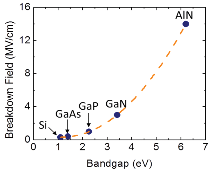
In addition, the wurtzite crystal structure of GaN exhibits robust spontaneous and piezoelectric polarization effects. At the interface of GaN, when a heterojunction is constructed with another material, AlGaN, a large polarization field will be induced. The field is generally larger than the breakdown field of GaN in Figure 1 and exhibits ultra-wide bandgap energy [6]. This effectively eliminates the need for additional doping and forms a highly concentrated two-dimensional electron plasma with a sheet density of up to 1013 cm−2. The bandgap of GaN has a negative temperature coefficient (0.4 meV/K). Namely, it slightly narrows with increasing temperature. However, the wide bandgap can always guarantee excellent thermal stability in GaN.
These exceptional band structure characteristics make GaN a superior material for applications such as blue/ultraviolet LEDs, laser diodes, 5G RF devices, and high-efficiency power electronics, solidifying its role as a cornerstone of next-generation semiconductor technology.
2.2. Optical properties
As one of the third-generation semiconductor materials, GaN exhibits unparalleled optical properties, making it the material of choice for most optoelectronic applications. In terms of optical absorption characteristics, GaN exhibits extremely high absorption coefficients of >10⁵ cm⁻¹ in the ultraviolet and visible light bands. This property is fundamentally attributed to the direct bandgap material characteristic of GaN. It is easy for electrons to transition between the valence band and conduction band under the action of photons without momentum compensation. This highly sensitive absorption characteristic makes GaN the guillotine material for ultraviolet photodetectors [7] with ultra-high sensitivity far exceeding traditional silicon devices [8].
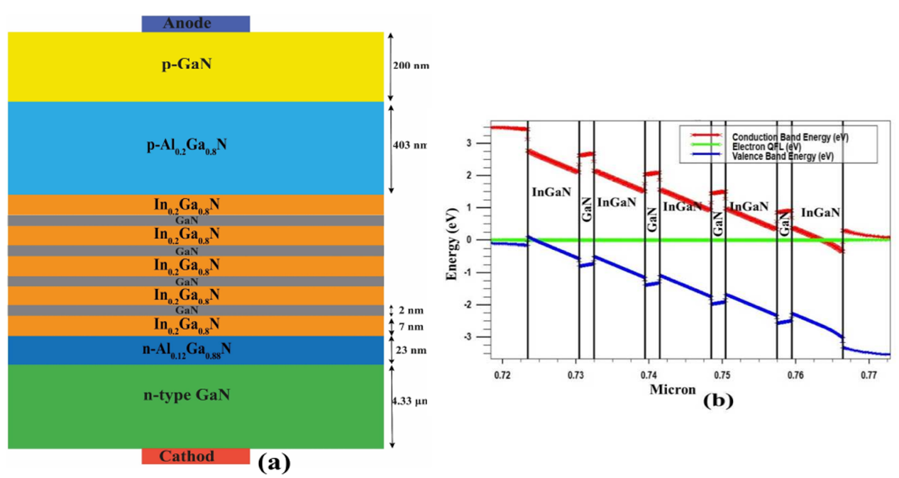
In terms of luminescence characteristics, the GaN material system exhibits excellent radiative recombination efficiency in blue and ultraviolet luminescence. In the luminescence wavelength range, through the design of InGaN/GaN MQW structures, precise controllable luminescence from the ultraviolet (365 nm) to green light (520 nm) wavelength can be achieved with extremely high luminescence efficiency. Modern blue GaN luminescent LEDs can achieve an ultra-high internal quantum efficiency of more than 80%, which cannot be achieved by traditional luminescent materials. More importantly, there is a unique defect tolerance in the luminescent material based on GaN, even if the dislocation density is as high as 10⁸–10⁹ cm⁻², excellent luminescent characteristics can still be maintained. This special characteristic is mainly due to the nanoscale composition spontaneously formed in InGaN quantum wells [9]. Fluctuations confine carriers, preventing carriers from diffusing to non-radiative defects and causing non-radiative recombination. As shown in Figure 2 [9], the fundamental structure of the MQW InGaN/GaN LED consists of a 4.33 µm Si-doped GaN substrate. On top of that, a 23 nm Si-doped Al0.12Ga0.88N layer (5×1018 cm⁻³) is added. In addition, the structure includes a 7 nm layer consisting of five In₀.₂Ga₀.₈N quantum wells (QWs). The wells are sandwiched between two AlGaN layers, where the top and bottom are p and n-type doped, respectively.
In addition, GaN’s high refractive index (around 2.4) brings extra benefits for device design in the optoelectronics field. When incorporated with the low-refraction-index material (e.g., SiO₂), strong optical confinement structures can be constructed to greatly improve the light extraction efficiency of LED devices. Regarding thermal stability, the bandgap temperature coefficient of GaN (-0.4 meV/K) is relatively small, rendering a stable optical performance in the high-temperature operating environment. Such excellent comprehensive nature makes GaN become the core material for the high-end optoelectronics applications represented by solid-state lighting, UV sterilization, and laser displays, and meanwhile promotes technological breakthroughs in the cutting-edge fields of deep-ultraviolet optoelectronic devices (Table 1).
|
Material |
Chemical Symbol |
Bandgap (300K, eV) |
Bandgap Temperature Coefficient (eV/K) |
Temperature Range (K) |
Features |
|
Gallium Nitride [1] |
GaN |
~3.4 (direct) |
-6.0 × 10⁻⁴ |
100–500 |
Wide bandgap, high thermal stability |
|
Silicon [1] |
Si |
~1.12 (indirect) |
-2.3 × 10⁻⁴ |
100–400 |
Traditional semiconductor |
|
Gallium Arsenide [2] |
GaAs |
~1.42 (direct) |
-4.5 × 10⁻⁴ |
100–500 |
High-frequency, optoelectronics |
|
Silicon Carbide (4H) [10] |
4H-SiC |
~3.26 (indirect) |
-3.3 × 10⁻⁴ |
100–700 |
High-temperature, high-power devices |
|
Indium Phosphide [11] |
InP |
~1.34 (direct) |
-3.7 × 10⁻⁴ |
100–500 |
Optoelectronics, high-frequency |
|
Zinc Oxide [12] |
ZnO |
~3.37 (direct) |
-8.0 × 10⁻⁴ |
100–500 |
UV optoelectronic devices |
|
Cadmium Sulfide [13] |
CdS |
~2.42 (direct) |
-4.1 × 10⁻⁴ |
100–500 |
Photoresistors, solar cells |
2.3. Electrical properties
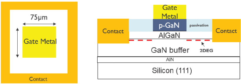
Due to the crystal's arrangement and 3.4 eV bandgap features, GaN exhibits distinct electrical capabilities in addition to its many optoelectronics-related traits. In terms of charge carrier transport, GaN demonstrates remarkable anisotropy: the electron mobility along the c-axis direction is approximately 1000 cm²/V·s, while in non-polar planes it can reach 2000 cm²/V·s, attributable to its relatively small electron effective mass (∼0.2m₀) at the conduction band minimum[5]. Particularly noteworthy is that in AlGaN/GaN heterostructures, the strong spontaneous and piezoelectric polarization effects (with polarization field strengths reaching MV/cm magnitudes) induce the formation of a high-density two-dimensional electron gas (2DEG) at the interface, which maintains room-temperature mobility in the range of 1500-2000 cm²/V·s and can still exceed 800 cm²/V·s even at elevated temperatures [14]. The cross-section and arrangement of the p-GaN/AlGaN/GaN capacitor are displayed in Figure 3. On a 200 mm silicon substrate, Metal-Organic Chemical Vapor Deposition (MOCVD) is used to produce these heterostructures. An epi stack comprising a 16 or 12.5 nm Al0.25Ga0.75N barrier layer, a GaN channel, a GaN buffer layer, and an AlN nucleation layer is developed on top of a 70 nm Mg-doped p-type GaN. To generate the final p-type GaN layer, two distinct Mg fluxes are employed
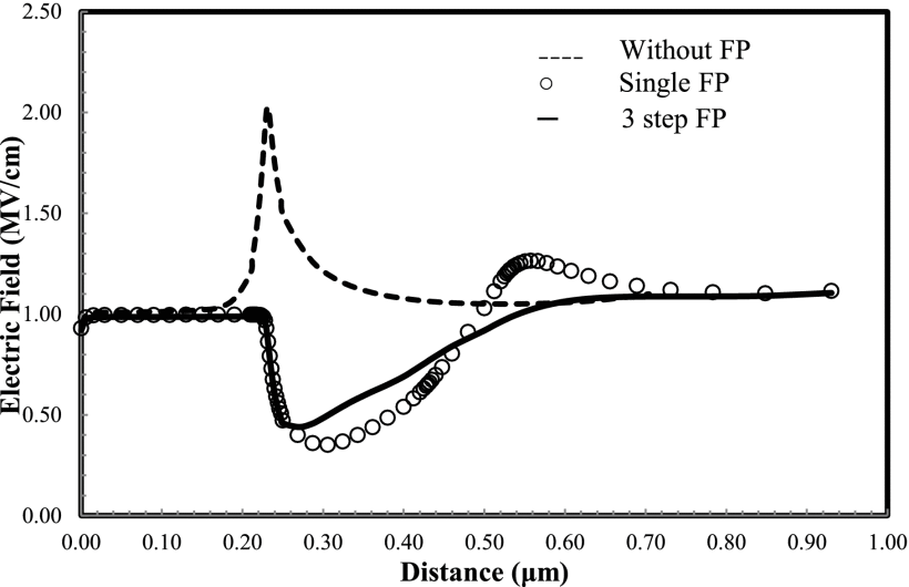
Due to its wide bandgap nature, but also significantly due to the large energy band offsets (conduction band offset ∼2.1 eV), GaN shows an extremely high critical breakdown field strength of 3.3 MV/cm. Compared to the Field Plate(FP) AlGaN/GaN HEMT architecture, shown in Figure 4, the electric field distribution along the channel length is higher. In FP architecture, the electric field is spread over the distance between the gate and the drain, which reduces the peak electric field at the drain-side gate edge and hence increases the breakdown voltage [15]. This high breakdown field allows GaN devices to realize an excellent Baliga figure of merit (theoretically 3000 times higher than Si), making it possible to design high-voltage devices with low conduction losses.
Highly asymmetric doping characteristics: n-doping (usually Si) shows great efficiency with an electron concentration up to 10¹⁹ cm⁻³ at room temperature, Si, with its low diffusivity, high activation efficiency, and low ionization energy, is the best choice for n-type doping of GaN [16], while p-type doping (usually Mg) is greatly limited due to the relatively deep acceptor level (~160 meV), and the hole concentration cannot exceed 10¹⁸ cm⁻³ generally. Extremely low intrinsic carrier concentration (~10⁻¹⁰ cm⁻³ at room temperature) together with the relatively high thermal conductivity (1.3 W/(cm·K)) guarantee decent electrical stability even in high-temperature environments. These unique electrical properties make GaN an excellent material system for high-frequency and high-power electronic devices.
3. Applications of GaN in semiconductor lasers
3.1. Structure of GaN-based lasers
GaN-based laser diodes typically employ an InGaN/GaN MQW active region with a p-n junction design, featuring the following key structural components:
3.1.1. Substrate selection
Traditional GaN-based LED chips have six sides and are rectangular. The primary structure is made up of a sapphire substrate that is about 100 μm thick and a GaN epitaxial layer that is about 6 μm thick. The LED's light is produced in the MQW when an electric current is introduced into the LED chip. The light travels through the GaN/Air and Sapphire/Air interfaces and emits forth. Since GaN and sapphire substrates have refractive indices that are significantly higher than those of air (nGaN∼2.5,nsapphire∼1.8,nair=1), total internal reflection on the GaN/Air and Sapphire/Air interfaces happens with ease. The critical angles of GaN/Air and Sapphire/Air are 23.5° and 33.7°, respectively, based on Snell's law (n1×sinθC=nair×sinθair) [17].
3.1.2. N-type region
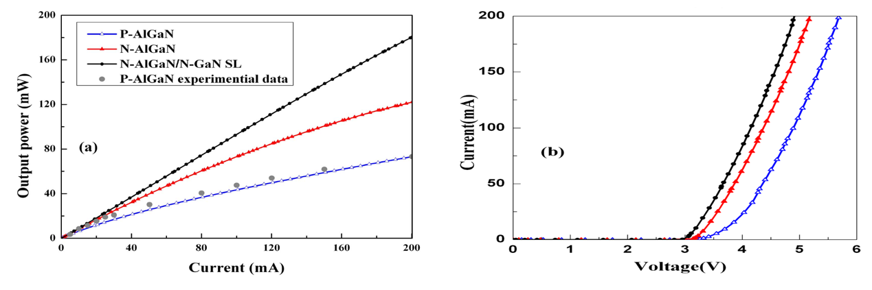
The two components of the N-type area are the silicon-doped In-GaN layer (5×10¹⁸ cm⁻³) and the n-AlGaN electron confinement layer, which is 2–5 μm thick. This area is frequently utilized for optical confinement and electron injection. Figure 5 (a) illustrates that the light output power increases by 146% and 69%, respectively, when the p-AlGaN EBL is removed and the n-AlGaN/n-GaN SL EBL or n-AlGaN is situated between the active region and the n-GaN layer [18]. The three devices' I-V curves in Figure 5(b) demonstrate that the LEDs with N-AlGaN/N-GaN SL EBL and N-AlGaN EBL have some improvement in terms of carrier transport, as seen by the drop in on-state voltage and series resistance.
3.1.3. P-type region
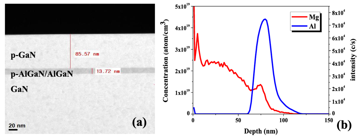
Polarization engineering or superlattice structures are typically employed to address the hole injection issue. Additional solutions to this issue include the p-AlGaN hole confinement layer and the p-GaN contact layer (Mg-doped, 1×10¹⁹ cm⁻³). A transmission electron microscope (TEM) picture in cross-section is displayed in Figure 6(a). Approximately 2×1019 cm3 and 1×1019 cm3 of magnesium doping are present in the p-GaN and p-AlGaN areas, respectively, based on the secondary ion mass spectrometry (SIMS) analysis shown in Figure 6(b) [19]. Diffusion during epitaxial growth has not been shown to significantly alter the distributions of Mg and Al doping.
3.1.4. Active region
The core structure features eight periods of InGaN/GaN MQWs [20], where each period is designed with a 3-nm InGaN QW and a 13-nm GaN barrier, ensuring effective carrier confinement and optical emission. The growth temperatures were 705°C and 850 °C for QWs and QBs, respectively [21]. Emission wavelength (450-530 nm) is controlled by indium content (15-20%). Radiative recombination efficiency is maximized using strain engineering.
3.1.5. Optical cavity
Dry etching was used to create the Fabry-Pérot resonator, which has a cavity length of 300–1000 μm. Optical feedback is provided by High-Reflection/ Anti-Reflection coatings on facets. Newer designs use vertical-cavity surface-emitting lasers (VCSELs) or distributed feedback combinations. GaN-based resonant cavity light-emitting diodes (RCLEDs)and VCSELs provide superior directionality, shorter linewidths, more stable peak wavelengths, and higher output coupling efficiency[21] when compared to traditional LEDs. A distributed Bragg reflector can also be used to manufacture GAN-based RCLEDs [22].
3.2. Application fields of GaN in semiconductor lasers
GaN-based semiconductor lasers have found widespread applications across multiple fields due to their outstanding performance, primarily in the following areas:
3.2.1. Blue/ultraviolet lasers
The substantial improvement in GaN crystal quality enabled researchers to control the conductivity of both p- and n-type nitride semiconductors, which made it possible to fabricate the high-brightness GaN-based p–n junction blue-LED and the high-performance violet/blue LD [23]. GaN-based semiconductor lasers have been widely used in various fields because of their remarkable performance mainly in the following three fields. The first one is Data Storage: Due to its short wavelength, the 405 nm blue-violet laser is the main light source for the Blu-ray/HD-DVD system (the currently available technology), with a much larger storage volume (>50 GB single disc) due to its short wavelength. The second one is the laser display: It is already applied in laser TVs and movie projection systems, which are enabled by 450 nm blue lasers and phosphor conversion. The third one is Optical Communication: GaN UV laser can realize short-range atmospheric optical communication with a modulation bandwidth at the GHz level.
3.2.2. High-power lasers
Automotive Applications is one industry. GaN blue lasers (450–470 nm) enable next-generation laser headlights that offer ultra-bright (>100,000 lux), energy-efficient illumination with flawless beam control. Light Detection and Ranging (LiDAR) systems that use pulsed GaN lasers (905 nm via frequency doubling) provide autonomous vehicles with long-range, high-resolution 3D sensing, enhancing object detection in low-visibility scenarios. Despite being relatively new, LiDAR sensors are finding widespread use in automotive applications due to their ability to offer high resolution, real-time 3D colorful point clouds of surroundings in low visibility settings with a long and wide detecting range [24]. They are therefore the next development in the direction of complete driverless capabilities [25]. Another industry is communication technology. Monolithically integrated PDs in InGaN/GaN LEDs are frequently used to track variations in LED intensity over time, which can significantly increase the optical power stability of LEDs. When it comes to high-speed modulation and high-brightness lighting, LDs perform noticeably better than LEDs. Using the same InGaN/GaN multi-QW active area, a waveguide PD with an edge-emitting LD was designed. An integrated PD-LD device can be built if it can be produced on a single chip. By integrating a waveguide PD (WPD) on a semi-polar GaN substrate, a skilled research team in China has now effectively produced such a device [26].
3.3. Advantages and challenges of GaN in semiconductor lasers
GaN has emerged as a key material for semiconductor lasers, particularly in the blue and UV wavelength ranges. GaN's unique properties offer several advantages but also present challenges in device fabrication and performance.
Advantages of GaN in Semiconductor Lasers: Initially, the wide bandgap (3.4 eV for GaN and 6 eV for AlGaN): GaN is the most promising material for UV, blue, green, and white high-brightness LEDs [27], which are essential for devices like optical storage, laser projectors, and Blu-ray discs. A greater voltage of breakdown than conventional III-V materials. Second, high efficiency & power output: molecular beam epitaxy's AlGaN-delta-GaN QW structure, which was constructed using a conventional AlN/sapphire template, showed a high internal quantum efficiency (85%) [28]. High-power continuous-wave (CW) and pulsed operation capabilities make it valuable for LiDAR, medical lasers, and industrial cutting [24]. Third, Thermal and Chemical Stability: GaN-based lasers reduce thermal droop and have superior thermal conductivity (130 W/m·K) compared to GaAs (50 W/m·K). They are appropriate for extreme environments and aerospace because they are resistant to radiation damage.
GaN Semiconductor Lasers also have many key challenges: Material flaws are one issue: High defect density: efficiency is decreased by heteroepitaxy-induced dislocations (10⁸–10¹⁰ cm⁻²). Inadequate p-type doping: high driving voltage results from low magnesium activation efficiency. "Green gap": Because of InGaN phase separation, efficiency drastically decreases beyond 530 nm. Thermal issues are another issue. Efficiency droop: performance is deteriorated by carrier leakage at high current. Local heating: without sophisticated cooling, temperatures in the active region can reach 150°C. Thermal stress: In high-power operation, cracking results from a mismatch in the coefficient of thermal expansion. High costs are the final problem: expensive substrates(silicon costs more than $100 for GaN native wafers). Complex fabrication: Gold-heavy connections and dry etching are needed for mirrors. Testing overhead: to validate reliability, about 1000 hours of burn-in are required.
4. Conclusion
To sum up, as a third-generation semiconductor, GaN has a wide bandgap (3.4 eV), a high breakdown field strength, and excellent chemical stability, enabling efficient UV-to-blue/green emission. Because GaN has a direct bandgap and high internal quantum efficiency (>80%), it is particularly suitable for short-wavelength laser applications, providing efficient high-power output without the need for frequency conversion. In laser applications, GaN’s high thermal conductivity (130 W/m·K) facilitates heat dissipation. However, there remain multiple challenges, such as efficiency droop and difficulty in p-type doping. State-of-the-art heat management and optical performance improvement methods, such as microfluidic cooling and nano-patterned surfaces, enable performance optimization. GaN lasers have already been widely commercialized in optical storage (Blu-ray), laser displays, and LiDAR. They also have great potential in visible light communication and medical UV sources.
The future of GaN technology will be centered around three development directions. Efficiency improvement: optimized epitaxial growth techniques, especially p-GaN doping and dislocation reduction, to reduce efficiency droop and improve light output; cost reduction: mass production and cost reduction using large-scale GaN-on-Si and GaN-on-diamond technologies; application expansion: advanced Micro-LEDs for augmented reality/virtual reality displays, quantum dot lasers for tunable visible-light emission for communications and sensing applications.
References
[1]. Zhang, L., Liu, P., Guo, S. and Huang, A.Q. (2016) Comparative study of temperature sensitive electrical parameters (tsep) of Si, SiC and GaN power devices. IEEE, 302-307.
[2]. Jena, D., Sahu, A.K., Das, S. and Sahoo, N. (2024) Study on optical properties of multiple quantum well-based InGaN/GaN light emitting diode. IEEE, 1-4.
[3]. Piotrowicz, S., Ouarch, Z., Chartier, E., Aubry, R., Callet, G., Floriot, D., Jacquet, J.C., Jardel, O., Morvan, E., Reveyrand, T., Sarazin, N. and Delage, S.L. (2010) 43W, 52% PAE X-band AlGaN/GaN HEMTs MMIC amplifiers. IEEE, 1-1.
[4]. Okumura, H., Malinverni, M., Martin, D. and Grandjean, N. (2016) High p-type GaN for advanced optoelectronic devices. IEEE, 661-662.
[5]. Elshtwy, N.A. and Ikraiam, F.A. (2024) Electron mobility calculations and scattering effects in GaN compound semiconductor. IEEE, 353-358.
[6]. Razzak, T., Xue, H., Xia, Z., Hwang, S., Khan, A., Lu, W. and Rajan, S. (2018) Ultra-wide band gap materials for high frequency applications. IEEE, 1-3.
[7]. Alpert, H.S., Yalamarthy, A.S., Satterthwaite, P.F., Jens, E., Rabinovitch, J., Scandrette, N., Newaz, A., Karp, A.C. and Senesky, D.G. (2019) Gallium nitride photodetector measurements of UV emission from a gaseous CH4/O2 hybrid rocket igniter plume. IEEE, 1-8.
[8]. Li, Y., Xiao, K., Lin, Z., Chen, K., Zou, J., Ye, S., Liang, H. and Mei, Z. (2025) High-performance ultraviolet photodetectors based on Ga2O3/GaN gradient heterojunction. IEEE Transactions on Electron Devices, 72(8), 4226-4231.
[9]. Yang, R., Zhang, J., Ma, H.-P. and Zhang, Q.-C. (2023) First principles studies for electronic structure of β-Ga2O3 and GaAs. IEEE, 177-180.
[10]. Wang, X.-R., Zhang, J., Ma, H.-P. and Zhang, Q.-C. (2023) Electrical characterization of HfO2/4H-SiC and HfO2/Si MOS structures. IEEE, 34-37.c
[11]. Barua, S., Abdulla-Al-Galib, M., Salam, K.M.A., Awal, M.A. and Wijesundera, R.P. (2012) Improved efficiency of photovoltaic cell based on indium-phosphide-oxide, indium-phosphide, indium-gallium arsenide and indium-gallium-antimonide. IEEE, 1-4.
[12]. Hussain, B., Raja, M.Y.A., Lu, N. and Ferguson, I. (2013) Applications and synthesis of zinc oxide: An emerging wide bandgap material. IEEE, 88-93.
[13]. Kumari, I.D., Jayasumana, S. and Attygalle, D. (2019) Development of a photosensor based on photo dielectric effect of cadmium sulphide. IEEE, 349-353.
[14]. Wu, T.-L., Bakeroot, B., Liang, H., Posthuma, N., You, S., Ronchi, N., Stoffels, S., Marcon, D. and Decoutere, S. (2017) Analysis of the gate capacitance-voltage characteristics in p-GaN/AlGaN/GaN heterostructures. IEEE Electron Device Letters, 38(12), 1696-1699.
[15]. Neha, Kumari, V., Gupta, M. and Saxena, M. (2018) Simulation based breakdown voltage analysis of 3-step field plate AlGaN/GaN HEMTs. IEEE, 169-173.
[16]. Baharin, A., Kocan, M., Umana-Membreno, G.A., Mishra, U.K., Parish, G. and Nener, B.D. (2008) Experimental and numerical investigation of the electrical characteristics of vertical n-p junction diodes created by Si implantation into p-GaN. IEEE, 12-15.
[17]. Chen, K.C., Su, Y.K., Lin, C.-L. and Hsu, H.C. (2011) Laser scribing of sapphire substrate to increase side light extraction of GaN-based light emitting diodes. Journal of Lightwave Technology, 29(13), 1907-1912.
[18]. Yu, X., Fan, G., Zheng, S., Ding, B. and Zhang, T. (2014) Performance of blue LEDs with N-AlGaN/N-GaN superlattice as electron-blocking layer. IEEE Photonics Technology Letters, 26(11), 1132-1135.
[19]. Kim, D.-G., Yim, J.-H., Lee, M.-K., Chae, M.-S., Kim, H. and Cha, H.-Y. (2024) P-GaN/p-AlGaN/AlGaN/GaN heterojunction field-effect transistor with a threshold voltage of 6 V. IEEE Electron Device Letters, 45(6), 972-975.
[20]. Chen, L., Wang, W. and Li, G. (2025) High-responsivity flexible InGaN/GaN MQWs nanomembrane photodetectors with DBR mirror toward visible light communication. IEEE Electron Device Letters, 46(2), 219-222.
[21]. Wu, H., Li, H., Kuo, S.-Y., Chen, B.-Y., Lu, T.-C. and Huang, H. (2020) High output power GaN-based green resonant-cavity light-emitting diodes with trapezoidal quantum wells. IEEE Transactions on Electron Devices, 67(9), 3650-3654.
[22]. Li, C., Feng, M., Liu, J., Liu, W., Sun, X., Liu, J., Sun, Z., Zhu, G., Zhang, S., Sun, Q. and Yang, H. (2025) GaN-based resonant-cavity light-emitting diode towards a vertical-cavity surface-emitting laser. IEEE Journal of Selected Topics in Quantum Electronics, 31(2), 1-6.
[23]. Akasaki, I. (2013) GaN-based p–n junction blue-light-emitting devices. Proceedings of the IEEE, 101(10), 2200-2210.
[24]. Liu, Y., Li, S., He, J., Hu, C., He, B., Krishnamurthy, K. and Shen, A. (2025) High-power and high-speed multi-channel VCSEL arrays with GaN driver for automotive LiDAR. IEEE, 3129-3132.
[25]. Behroozpour, B., Sandborn, P.A.M., Wu, M.C. and Boser, B.E. (2017) Lidar system architectures and circuits. IEEE Communications Magazine, 55(10), 135-142.
[26]. Yi, S., Hu, J. and Shen, C. (2023) Recent advances of III-nitride integrated photonics technology for visible light applications. IEEE, 1-2.
[27]. DenBaars, S.P., Katona, T., Cantu, P., Hanlon, A., Keller, S., Schmidt, M., Margalith, T., Pattisson, M., Moe, C., Speck, J. and Nakamura, S. (2003) GaN based high brightness LEDs and UV LEDs. IEEE, 16.1.1-16.1.3.
[28]. Liu, C., Lee, K., Harden, G., Hoffman, A., Xing, H.G., Jena, D. and Zhang, J. (2020) High internal quantum efficiency from AlGaN-delta-GaN quantum well at 260 nm. IEEE, 1-2.
Cite this article
Shi,H. (2025). The Photoelectric Properties of Gallium Nitride Materials and Applications in Semiconductor Lasers. Applied and Computational Engineering,180,22-32.
Data availability
The datasets used and/or analyzed during the current study will be available from the authors upon reasonable request.
Disclaimer/Publisher's Note
The statements, opinions and data contained in all publications are solely those of the individual author(s) and contributor(s) and not of EWA Publishing and/or the editor(s). EWA Publishing and/or the editor(s) disclaim responsibility for any injury to people or property resulting from any ideas, methods, instructions or products referred to in the content.
About volume
Volume title: Proceedings of CONF-MCEE 2026 Symposium: Advances in Sustainable Aviation and Aerospace Vehicle Automation
© 2024 by the author(s). Licensee EWA Publishing, Oxford, UK. This article is an open access article distributed under the terms and
conditions of the Creative Commons Attribution (CC BY) license. Authors who
publish this series agree to the following terms:
1. Authors retain copyright and grant the series right of first publication with the work simultaneously licensed under a Creative Commons
Attribution License that allows others to share the work with an acknowledgment of the work's authorship and initial publication in this
series.
2. Authors are able to enter into separate, additional contractual arrangements for the non-exclusive distribution of the series's published
version of the work (e.g., post it to an institutional repository or publish it in a book), with an acknowledgment of its initial
publication in this series.
3. Authors are permitted and encouraged to post their work online (e.g., in institutional repositories or on their website) prior to and
during the submission process, as it can lead to productive exchanges, as well as earlier and greater citation of published work (See
Open access policy for details).
References
[1]. Zhang, L., Liu, P., Guo, S. and Huang, A.Q. (2016) Comparative study of temperature sensitive electrical parameters (tsep) of Si, SiC and GaN power devices. IEEE, 302-307.
[2]. Jena, D., Sahu, A.K., Das, S. and Sahoo, N. (2024) Study on optical properties of multiple quantum well-based InGaN/GaN light emitting diode. IEEE, 1-4.
[3]. Piotrowicz, S., Ouarch, Z., Chartier, E., Aubry, R., Callet, G., Floriot, D., Jacquet, J.C., Jardel, O., Morvan, E., Reveyrand, T., Sarazin, N. and Delage, S.L. (2010) 43W, 52% PAE X-band AlGaN/GaN HEMTs MMIC amplifiers. IEEE, 1-1.
[4]. Okumura, H., Malinverni, M., Martin, D. and Grandjean, N. (2016) High p-type GaN for advanced optoelectronic devices. IEEE, 661-662.
[5]. Elshtwy, N.A. and Ikraiam, F.A. (2024) Electron mobility calculations and scattering effects in GaN compound semiconductor. IEEE, 353-358.
[6]. Razzak, T., Xue, H., Xia, Z., Hwang, S., Khan, A., Lu, W. and Rajan, S. (2018) Ultra-wide band gap materials for high frequency applications. IEEE, 1-3.
[7]. Alpert, H.S., Yalamarthy, A.S., Satterthwaite, P.F., Jens, E., Rabinovitch, J., Scandrette, N., Newaz, A., Karp, A.C. and Senesky, D.G. (2019) Gallium nitride photodetector measurements of UV emission from a gaseous CH4/O2 hybrid rocket igniter plume. IEEE, 1-8.
[8]. Li, Y., Xiao, K., Lin, Z., Chen, K., Zou, J., Ye, S., Liang, H. and Mei, Z. (2025) High-performance ultraviolet photodetectors based on Ga2O3/GaN gradient heterojunction. IEEE Transactions on Electron Devices, 72(8), 4226-4231.
[9]. Yang, R., Zhang, J., Ma, H.-P. and Zhang, Q.-C. (2023) First principles studies for electronic structure of β-Ga2O3 and GaAs. IEEE, 177-180.
[10]. Wang, X.-R., Zhang, J., Ma, H.-P. and Zhang, Q.-C. (2023) Electrical characterization of HfO2/4H-SiC and HfO2/Si MOS structures. IEEE, 34-37.c
[11]. Barua, S., Abdulla-Al-Galib, M., Salam, K.M.A., Awal, M.A. and Wijesundera, R.P. (2012) Improved efficiency of photovoltaic cell based on indium-phosphide-oxide, indium-phosphide, indium-gallium arsenide and indium-gallium-antimonide. IEEE, 1-4.
[12]. Hussain, B., Raja, M.Y.A., Lu, N. and Ferguson, I. (2013) Applications and synthesis of zinc oxide: An emerging wide bandgap material. IEEE, 88-93.
[13]. Kumari, I.D., Jayasumana, S. and Attygalle, D. (2019) Development of a photosensor based on photo dielectric effect of cadmium sulphide. IEEE, 349-353.
[14]. Wu, T.-L., Bakeroot, B., Liang, H., Posthuma, N., You, S., Ronchi, N., Stoffels, S., Marcon, D. and Decoutere, S. (2017) Analysis of the gate capacitance-voltage characteristics in p-GaN/AlGaN/GaN heterostructures. IEEE Electron Device Letters, 38(12), 1696-1699.
[15]. Neha, Kumari, V., Gupta, M. and Saxena, M. (2018) Simulation based breakdown voltage analysis of 3-step field plate AlGaN/GaN HEMTs. IEEE, 169-173.
[16]. Baharin, A., Kocan, M., Umana-Membreno, G.A., Mishra, U.K., Parish, G. and Nener, B.D. (2008) Experimental and numerical investigation of the electrical characteristics of vertical n-p junction diodes created by Si implantation into p-GaN. IEEE, 12-15.
[17]. Chen, K.C., Su, Y.K., Lin, C.-L. and Hsu, H.C. (2011) Laser scribing of sapphire substrate to increase side light extraction of GaN-based light emitting diodes. Journal of Lightwave Technology, 29(13), 1907-1912.
[18]. Yu, X., Fan, G., Zheng, S., Ding, B. and Zhang, T. (2014) Performance of blue LEDs with N-AlGaN/N-GaN superlattice as electron-blocking layer. IEEE Photonics Technology Letters, 26(11), 1132-1135.
[19]. Kim, D.-G., Yim, J.-H., Lee, M.-K., Chae, M.-S., Kim, H. and Cha, H.-Y. (2024) P-GaN/p-AlGaN/AlGaN/GaN heterojunction field-effect transistor with a threshold voltage of 6 V. IEEE Electron Device Letters, 45(6), 972-975.
[20]. Chen, L., Wang, W. and Li, G. (2025) High-responsivity flexible InGaN/GaN MQWs nanomembrane photodetectors with DBR mirror toward visible light communication. IEEE Electron Device Letters, 46(2), 219-222.
[21]. Wu, H., Li, H., Kuo, S.-Y., Chen, B.-Y., Lu, T.-C. and Huang, H. (2020) High output power GaN-based green resonant-cavity light-emitting diodes with trapezoidal quantum wells. IEEE Transactions on Electron Devices, 67(9), 3650-3654.
[22]. Li, C., Feng, M., Liu, J., Liu, W., Sun, X., Liu, J., Sun, Z., Zhu, G., Zhang, S., Sun, Q. and Yang, H. (2025) GaN-based resonant-cavity light-emitting diode towards a vertical-cavity surface-emitting laser. IEEE Journal of Selected Topics in Quantum Electronics, 31(2), 1-6.
[23]. Akasaki, I. (2013) GaN-based p–n junction blue-light-emitting devices. Proceedings of the IEEE, 101(10), 2200-2210.
[24]. Liu, Y., Li, S., He, J., Hu, C., He, B., Krishnamurthy, K. and Shen, A. (2025) High-power and high-speed multi-channel VCSEL arrays with GaN driver for automotive LiDAR. IEEE, 3129-3132.
[25]. Behroozpour, B., Sandborn, P.A.M., Wu, M.C. and Boser, B.E. (2017) Lidar system architectures and circuits. IEEE Communications Magazine, 55(10), 135-142.
[26]. Yi, S., Hu, J. and Shen, C. (2023) Recent advances of III-nitride integrated photonics technology for visible light applications. IEEE, 1-2.
[27]. DenBaars, S.P., Katona, T., Cantu, P., Hanlon, A., Keller, S., Schmidt, M., Margalith, T., Pattisson, M., Moe, C., Speck, J. and Nakamura, S. (2003) GaN based high brightness LEDs and UV LEDs. IEEE, 16.1.1-16.1.3.
[28]. Liu, C., Lee, K., Harden, G., Hoffman, A., Xing, H.G., Jena, D. and Zhang, J. (2020) High internal quantum efficiency from AlGaN-delta-GaN quantum well at 260 nm. IEEE, 1-2.