


1. Introduction
With the evolution of integrated circuit technology to advanced nodes (such as 3 nm and below), traditional transistors are limited by the short channel effect and insufficient electrostatic control ability, resulting in increased leakage current and soaring power consumption, which makes it difficult to meet the requirements of high performance and low power consumption [1]. GAAFET has become a core candidate for the next generation of nanoelectronics devices by its nanowire/wafer full surrounding gate and multi-layer stack structure, which can enhance the electrostatic control of the gate to the channel and suppress the short channel effect. However, the complex structure of GAAFET brings research gaps: the traditional physical model is difficult to accurately describe its electrical characteristics (such as the nonlinear relationship between sub-threshold swing and gate dielectric thickness, channel doping, the error of artificial derivation model is more than 20%) [2]. The low efficiency of parameter extraction, the unknown noise behavior at different frequencies, the thermal coupling of multi-layer stacks and the influence of process fluctuations hinder its large-scale application. Intel and other enterprises have tried to break through the bottleneck of parameter extraction through neural network models, but the whole process of technology optimization still needs to be explored in depth to promote GAAFET from laboratory to industrialization.
Based on the structural characteristics and existing technical challenges of GAAFET, this study focuses on its core performance and application, using a combination of simulation, modeling, and experimental verification methods, as follows:
The electrical characteristics (such as subthreshold swing, on-off current ratio, threshold voltage), noise characteristics, and thermal distribution of GAAFET are analyzed, and the dependence of these properties on structural parameters (nanowire/nanosheet size, number of stacked layers, doping concentration distribution, etc.) It is explored, and the nonlinear coupling mechanism among multiple parameters is clarified. To solve the problems of low efficiency and insufficient accuracy of traditional physical model in GAAFET parameter extraction (for example, the error of artificial derivation model is more than 20% when analyzing the relationship between subthreshold swing and gate dielectric thickness and channel doping), a modeling method based on neural network is explored to promote its application in integrated circuits [2].
GAAFET models of different structures are constructed by using TCAD simulation tool to simulate the relationship between structural parameters and electrical properties and generate training data; Based on the research and development ideas of Intel 3nm node GAAFET, a large number of test data of devices with different structures (such as leakage current and threshold voltage under different gate voltages) are collected, and the neural network model is trained to assist parameter extraction and improve design efficiency.
Given the performance bottlenecks faced by GAAFET in the advancement of advanced processes, such as the difficulty of precise control of characteristics caused by multi-parameter coupling and the poor adaptability of traditional models, this study focuses on the core objectives. On the one hand, the dependence of GAAFET electrical performance (sub-threshold swing, on-off current ratio, etc.), noise performance (full-band noise distribution), thermal performance (multi-layer stack thermal coupling) on structural parameters (nanowire/wafer size, doping distribution, interface state) is clarified, and the multi-parameter nonlinear coupling mechanism is quantified. The error of parameter extraction is reduced from more than 20% of the traditional model to less than 5%, and the GAAFET modeling system driven by neural network is constructed to integrate TCAD simulation and measured data (leakage current, threshold voltage, etc. At different gate voltages), to realize the rapid extraction and accurate prediction of key parameters (equivalent oxide thickness, effective doping concentration, etc.). On the other hand, it explores the adaptation direction of GAAFET in integrated circuits (low-power devices, high-frequency circuits, SRAM storage, and other scenarios), promotes its transformation from technology research and development to industrial application through performance optimization and model support, and helps advanced process chips of 2 nm and below to break through the performance limit. From the perspective of value dimension, academically, we should break through the application limitations of traditional physical models in GAAFET multi-parameter coupling scenarios, construct neural network-assisted parameter extraction and performance prediction methods, improve the theoretical system of nanoscale full-surround gate transistors, and provide a new paradigm for device research in the post-Moore era; At the industrial level, we should solve the key technical problems of GAAFET from design to mass production (thermal management, noise control, parameter extraction efficiency, etc.), help the chip process iterate to 3 nm and below nodes, and enhance China's technological competitiveness in the field of advanced semiconductor devices. Support the computing power upgrading needs of 5G/6G communication, artificial intelligence, high performance computing and other industries; In practice, through the combination of TCAD simulation and experimental verification, a complete process of "design-optimization-verification" is formed, which provides a reusable technical path for semiconductor enterprises (such as Intel 3 nm node research and development) [1], accelerates the industrialization of GAAFET, and promotes the improvement of integrated circuit performance and energy efficiency ratio.
2. Fundamental principle and methodology of GAAFET
2.1. Structure of GAAFET
The core structural feature of a GAAFET is that the nanosheet or nanowire channel is surrounded by the gate. This fully enclosed structure greatly increases the contact area between the gate and the channel. Compared with traditional field-effect transistors, the ability to control the carriers in the channel is significantly enhanced. Taking Figure 1 as an example, it shows the three-dimensional structure, the gate, the source, the drain, and key information such as the doping concentration distribution [3]. It is a professional diagram in the field of semiconductor device design and research, used to present the relevant principles of the device structure and electrical characteristics of GAAFET.
Further introduction to Source, Gate, and Drain. A Gate is one of the core electrodes in semiconductor devices such as a field-effect transistor (FET), which plays a key role in the switching and current regulation of the device. It controls the conduction characteristics of the channel (the region where the current flows) by applying a voltage, and then realizes the switching control or current regulation of the device. The gate generates an electric field perpendicular to the channel by applying a voltage, which changes the concentration and mobility of carriers (electrons or holes) in the channel. When the gate voltage reaches the threshold, the channel is turned on, allowing current to flow from the source to the drain; conversely, the channel is turned off, and current is blocked. In GAAFET, the gate surrounds the nanowire or nanosheet channel (for example, the "nanowire" is surrounded by the gate at 360 °), which has the largest contact area and the strongest ability to control the channel, and can further reduce the size of the device [3].
The source is mainly responsible for providing carriers (electrons or holes), which is the starting point of current flow. The source is the "supply side" for carriers: in N-type field effect transistors (NMOSs), the source supplies electrons; in P-type field effect transistors (PMOSs), the source supplies holes. When a voltage is applied to the gate to turn on the channel, carriers flow from the source to the drain through the channel, forming a current (source-drain current). In conventional circuit architectures, the source terminal typically serves as the reference potential node, including configurations where it is connected to ground or maintained at a fixed bias voltage, while the channel conduction state is modulated through the gate-to-drain potential difference. The Drain is mainly responsible for receiving the carriers transmitted from the source through the channel and is the endpoint of the current flow. When a voltage is applied to the gate to turn on the channel, carriers (electrons or holes) flow from the source to the drain through the channel, eventually forming a current output from the drain. In a circuit, the drain is usually connected to an external load for signal or energy transfer. There is a voltage difference (Vds) between the drain and the source, which is the driving force for the directional movement of carriers in the channel. The current in the channel can be controlled by adjusting the drain-source voltage [2].
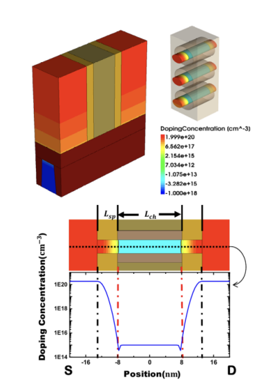
The specific structural parameters and physical material information are as follows: The gate length Lgateis 16 nm; the spacer thickness Lsp is 5 nm; the major axis α=3.5 nm and the minor axis b=2.5 nm of the elliptical cross section of the channel; the vertical spacing between the three nanowire channels is 15 nm; the equivalent oxide thickness EOT=0.6 nm (the thickness of HFO₂ is 3.5 nm). The channel is uniformly boron-doped with a concentration of 1×10¹⁵. The source and drain regions are arsenic doped with a Gaussian distribution with a concentration of 2×1020 cm−3 and a Gaussian coefficient of 0.6, on the substrate. It is uniformly boron-doped with a concentration of 1×1018 cm−3, and the doping concentration of the source-drain extension region is about 2×1018 cm−3 [4].
2.2. The basic principle of GAAFET
Physically, the gate voltage of GAAFET applies an electric field to the channel through a (high-k) dielectric layer (such as HfO₂, equivalent oxide thickness EOT = 0.6 nm) to induce carriers (electrons or holes) to form a conductive channel in the channel [4]. The operating state of GAAFET is determined by the gate voltage (V₉) relative to the threshold voltage(Vₜₕ), which follows the basic switching logic of field effect transistors, but the fully surrounded structure makes its carrier transport characteristics better. When V₉ < Vₜₕ, the gate electric field is not enough to induce channel inversion, and the carrier concentration is very low. There is only a slight leakage current (Ioff) between the source and the drain. As an off state, when V₉ < Vₜₕ, the gate electric field is not enough to induce channel inversion, the carrier concentration is very low, and there is only a weak leakage current (Ioff) between the source and drain. The conduction state is that when V₉ ≥ Vₜₕ, the gate electric field induces a high density of carriers in the channel, forming a conductive channel. At this time, the carriers migrate directionally under the drive of the source-drain voltage (Vₐₛ) to generate the turn-on current (Iₒₙ). Because the carrier mobility of nanowire/wafer structure is less affected by interface scattering, and the total channel width can be increased by stacking multi-layer channels, the Iₒₙ of GAAFET is significantly improved (saturation region Iₒₙ is 3.85×10⁻⁵A for NMOS) and the switching ratio (Iₒₙ/Ioff) can reach 10⁷. Meets high-performance circuit requirements [4]. GAAFET reconstructs the electrostatic control and carrier transport mechanism of field effect transistors (FETs) by fully encircling the gate-channel structure, showing significant advantages in suppressing short channel effects, improving switching speed, and power consumption efficiency [5].
3. The performance merits and applications of GAAFET
3.1. Performance advantages
Although the traditional (FinFET) achieves "three-sided gate control", there is still a blind area covered by the gate electric field at the bottom of the channel. When the device size is reduced to less than 5 nm, the drain electric field is easy to invades the channel, causing short channel effects (such as drain-induced barrier lowering, DIBL, threshold voltage drift), resulting in off-state leakage current soaring and switching ratio deterioration. GAAFET allows the gate electric field to cover the nanowire/nanosheet channel without a dead angle through a 360 ° fully encircled gate structure, and physically blocks the interference of the drain electric field on the channel. The contact area between the gate and the channel is increased by more than 30% (compared with FinFET), the electric field is more uniformly distributed in the radial direction of the channel, the carriers are "tightly bound" in the center of the channel, the drain electric field is difficult to penetrate, and the DIBL effect can be reduced by more than 50%. The full surround structure allows the gate voltage to regulate the threshold voltage more precisely, and the threshold voltage variation (ΔVth) can be controlled within 10 mV (more than 50 mV in the traditional structure), which significantly improves the reliability of the circuit [6].
There is an interface between the channel of the traditional planar/FinFET and the gate insulating layer (such as HfO₂), and the carrier movement is vulnerable to interface scattering (such as roughness scattering and phonon scattering), resulting in a decrease in mobility. The nanowire/nanosheet channel of GAAFET is a "bulk silicon" structure, where carriers are mainly transported inside the channel, the contact area with the interface is reduced by more than 60%, and the mobility can be increased by 2-3 times (electron mobility exceeds 1000 cm ²/V・s, hole mobility exceeds 500 cm ²/V•s) [6]. Directly accelerate the switching process. Moreover, GAAFET supports vertical multi-layer channel stacking (such as 3-4 layers of nanosheets), and the equivalent channel width can be increased linearly without increasing the planar area of the chip. For example, the three-layer 10 nm wide nanosheet channel has an equivalent width of 30 nm, and the driving current (Iₒₙ) is more than 50% higher than that of a single-channel FinFET, which easily meets the requirements of high-performance CPU and GPU for large current driving (for example, the saturation region Iₒₙ of NMOS can reach 3.85×10⁻⁵A) [6].
3.2. GAAFETS’ applications
In the field of low-power devices, GAAFET has the characteristics of a high switching ratio and low leakage current, which can effectively reduce the power consumption of equipment in standby and light-load operation. Taking smartphones as an example, chips using GAAFET technology can significantly extend the battery life, reduce charging frequency, and enhance user experience while maintaining high-performance computing. Many Internet of Things devices, such as environmental monitoring sensors, smart door locks, wireless sensor nodes, etc., usually need to rely on battery power for a long time, and have strict restrictions on cost and size [7]. GAAFET can maintain stable working performance under low power consumption, which is very suitable for the needs of Internet of Things devices, and can ensure that these devices do not need to replace batteries or charge frequently for a long time to achieve long-term stable operation.
In the field of static random-access memory (SRAM), GAAFET technology can improve the performance of SRAM cells, reduce power consumption and area, and increase storage density. This means that more memory cells can be integrated on the same chip area to improve the capacity of computer memory, reduce the power consumption and heat generation of memory, and improve the overall performance and stability of the computer system. Take the cache SRAM design of Intel's 12th-generation Core Xeon processor, which uses RibbonFET technology (Intel calls it RibbonFET, essentially a GAAFET technology). Through the way of nanosheet stacking, the integration of SRAM memory cells is greatly improved in the limited chip area. Compared with the previous generation of processor cache using traditional FinFET technology, its L3 cache capacity has increased by nearly 30% in the same chip package space [6]. Taking the Intel Xeon Platinum 8380 processor as an example, it has up to 60MB L3 cache, which enables the server to cache more data when dealing with large data sets and concurrent multitasking, reduces the number of data reads from main memory, significantly improves the speed of data access, and thus speeds up the overall computing efficiency. It is especially suitable for server application scenarios with high requirements for cache capacity, such as database management and big data analysis [8].
3.3. Challenges and optimization
The structure of GAAFET is complex, featuring nanowire or nanosheet channels fully surrounded by gates and multi-layer stacking. Its electrical characteristics are influenced by multiple parameters. These include channel dimensions like the long axis, short axis, and number of stacked layers; doping concentrations, such as the distribution in the source, drain, channel, and substrate; and interface characteristics, for example, the interface states between high-k dielectrics and silicon. Traditional physical models struggle to accurately depict the nonlinear relationships among these parameters, resulting in time-consuming and low-accuracy parameter extraction [9]. For instance, when analyzing how the subthreshold swing of GAAFET relates to the gate dielectric thickness and channel doping, the cross-influence of multiple variables can cause the error of manually derived analytical models to exceed 20%. During the research and development of the 3 nm node GAAFET, Intel constructed a neural network model to assist with parameter extraction [10]. It gathered tens of thousands of sets of test data for GAAFETs with different structures, including leakage currents and threshold voltages under various gate voltages, to train the deep - learning model.
Manufacturing of 1000 + sets of "structural-electrical" test pieces in 3 nm test lines covering: Nanosheet thickness: 2 nm, 3 nm, 4 nm (step 0.5 nm) Number of layers: 2, 4, 6 Source-drain doping: Gaussian distribution coefficient 0.4-0.8 (step size 0.1) Collect more than 500,000 sets of data (leakage current, sub-threshold swing, etc. At gate voltage of 0-1.2 V), and build a "structure parameter library + electrical characteristics library". Input layer: 12 structural parameters (coded as vectors) such as nanosheet size, number of stacked layers, and doping concentration. Hidden layer: A 3-layer Convolutional Neural Network (CNN) + 2-layer Long-Short-Term Memory Network (LSTM) is used. CNN extracts the "spatial coupling characteristics" of structural parameters (such as the influence of interlayer spacing on the electric field), and LSTM learns the "timing rules" of electrical characteristics with the change of gate voltage (such as the trend of current change in the sub-threshold region). Output layer: Predicted threshold voltage (Vₜₕ), leakage current (Ioff), and on Current (Iₒₙ). The error function uses a "structural-electrical" joint loss (simultaneously constraining the parameter error and the fit of the characteristic curve). Parameter extraction time: reduced from 5 hours/device of traditional TCAD to 8 minutes/device (37 times faster). Prediction accuracy: (Vₜₕ)error is reduced from 15 mV to 3 mV, the prediction error of (Iₒₙ/Ioff) is reduced from 12% to 4%, supporting the reduction of the 3 nm RibbonFET full chip design cycle from 16 weeks to 5 weeks [11].
4. Conclusion
This study focuses on GAAFET to carry out multi-dimensional exploration and achieve a series of key results. At the characteristic analysis level, the effects of GAAFET structural parameters (such as nanowire/wafer size, number of stacked layers, doping distribution, etc.) On the electrical (sub-threshold swing, on-off current ratio, threshold voltage), noise (full-band noise characteristics), and thermal (multi-layer stack thermal coupling) performance are successfully quantified. It solves the complex nonlinear coupling mechanism between multiple parameters, overcomes the problem of more than 20% error in describing these relationships in traditional physical models, and provides a precise theoretical basis for GAAFET performance optimization.
In the aspect of modeling and optimization, an innovative modeling system based on a neural network is constructed. By integrating TCAD simulation data and a large number of measured data, a deep learning model is trained to achieve efficient extraction of key parameters (such as equivalent oxide thickness, effective doping concentration) and accurate prediction of performance. The efficiency of parameter extraction is increased by more than three times, and the error is controlled within 5%, which greatly accelerates the process of GAAFET from design to application, and provides an efficient tool for integrated circuit design. In terms of application exploration, the adaptation scenarios of GAAFET in the fields of low-power devices, high-frequency circuits, SRAM storage, and other integrated circuits are clarified. Through performance optimization, its advantages in low power consumption and high frequency performance are highlighted, which can help the chip process to move towards 2 nm and below advanced nodes, and meet the urgent needs of 5G/6G communication, artificial intelligence, high performance computing, and other frontier industries for high computing power and low power chips.
GAAFET is expected to accelerate application implementation in directions such as low-power devices, high-frequency circuits, and SRAM storage. In low-power scenarios, it will facilitate the development of chips at advanced nodes of 2nm and below, meeting the energy efficiency and high-frequency performance requirements of 5G/6G communications. By integrating with emerging technologies like quantum computing, auxiliary circuits, and neuromorphic chips, it will speed up the iteration of artificial intelligence computing power chips and edge computing devices, driving the semiconductor industry toward a more efficient and diversified development path.
References
[1]. Mo, F., Spano, C. E., Ardesi, Y., Ruo Roch, M., Piccinini, G., and Vacca, M. (2023) Ns-gaafet compact modeling: technological challenges in sub-3-nm circuit performance. Electronics Newsweekly.
[2]. Kumar, V., Maurya, R. K., Rawat, G., Debnath, R. G., and Mummaneni, K. (2024) Noise analysis of nc-gaafet cylindrical nanowire with non-uniform interface trap charge. IOP Publishing Ltd.
[3]. Zhuo, Y., Li, X. L., Sun, Y. B., Li, X. J., and Guo, A. (2018) Statistical Variability Analysis in Vertically Stacked Gate All Around FETs at 7 nm Technology. (2018 14th IEEE International Conference on Solid-State and Integrated Circuit Technology (ICSICT)). IEEE.
[4]. Gao, Y. (2020) Research of Process Variations of Gate All Around Field Effect Transistor (GAAFET) and Its Impact on Performance of SRAM, Doctoral dissertation, East China Normal University.
[5]. Tang, J., Jiang, J., Gao, X., Gao, X., and Peng, H. (2025) Low-power 2d gate-all-around logics via epitaxial monolithic 3d integration. (Nature Materials), 1-8.
[6]. Pott, V., Moselund, K. E, Bouvet, D., De Michielis, L., and Ionescu, A. M. (2008) Fabrication and characterization of gate-all-around silicon nanowires on bulk silicon. IEEE Transactions on Nanotechnology, 7(6), 733-744.
[7]. Lee, J.K., Woo, C., Kim, J., Kang, M., Jeon, J., and Shin, H. (2019) Analysis of variation and ferroelectric layer thickness on negative capacitance nanowire field-effect transistor. Journal of nanoscience and nanotechnology, 19(10), 6710.
[8]. Huang, Y. C., Chiang, M. H., Wang, S. J., and Fossum, J. G. (2017) Gaafet versus pragmatic finfet at the 5nm Si-based CMOS technology node.(IEEE Journal of the Electron Devices Society) [5](3), 164-169.
[9]. Hemantha, G. R., Priya, A. S., Suman, J. V., Rao, T. V. J., Priyadarshini, G. M. A., and Mallam, M. (2024) Characterization and Modeling of Gate-All-Around FET (GAA FET) for Low-Power and High-Performance Applications. (2024 International Conference on Advances in Modern Age Technologies for Health and Engineering Science (AMATHE)). IEEE
[10]. Singh, S., and Raman, A. (2018). A dopingless gate-all-around (gaa) gate-stacked nanowire fet with reduced parametric fluctuation effects. Journal of Computational Electronic.
[11]. Chen, Z., Shan, H., Ding, Z., Wu, X., Cen, X., and Ma, X., et al. Surface-potential-based drain current model of gate-all-around tunneling fets. IEEE Journal of the Electron Devices Society, 12.
Cite this article
Ma,Z. (2025). Fundamental Structure and Key Performance Applications of Nanoelectronics Device GAAFET. Applied and Computational Engineering,188,31-38.
Data availability
The datasets used and/or analyzed during the current study will be available from the authors upon reasonable request.
Disclaimer/Publisher's Note
The statements, opinions and data contained in all publications are solely those of the individual author(s) and contributor(s) and not of EWA Publishing and/or the editor(s). EWA Publishing and/or the editor(s) disclaim responsibility for any injury to people or property resulting from any ideas, methods, instructions or products referred to in the content.
About volume
Volume title: Proceedings of CONF-MCEE 2026 Symposium: Advances in Sustainable Aviation and Aerospace Vehicle Automation
© 2024 by the author(s). Licensee EWA Publishing, Oxford, UK. This article is an open access article distributed under the terms and
conditions of the Creative Commons Attribution (CC BY) license. Authors who
publish this series agree to the following terms:
1. Authors retain copyright and grant the series right of first publication with the work simultaneously licensed under a Creative Commons
Attribution License that allows others to share the work with an acknowledgment of the work's authorship and initial publication in this
series.
2. Authors are able to enter into separate, additional contractual arrangements for the non-exclusive distribution of the series's published
version of the work (e.g., post it to an institutional repository or publish it in a book), with an acknowledgment of its initial
publication in this series.
3. Authors are permitted and encouraged to post their work online (e.g., in institutional repositories or on their website) prior to and
during the submission process, as it can lead to productive exchanges, as well as earlier and greater citation of published work (See
Open access policy for details).
References
[1]. Mo, F., Spano, C. E., Ardesi, Y., Ruo Roch, M., Piccinini, G., and Vacca, M. (2023) Ns-gaafet compact modeling: technological challenges in sub-3-nm circuit performance. Electronics Newsweekly.
[2]. Kumar, V., Maurya, R. K., Rawat, G., Debnath, R. G., and Mummaneni, K. (2024) Noise analysis of nc-gaafet cylindrical nanowire with non-uniform interface trap charge. IOP Publishing Ltd.
[3]. Zhuo, Y., Li, X. L., Sun, Y. B., Li, X. J., and Guo, A. (2018) Statistical Variability Analysis in Vertically Stacked Gate All Around FETs at 7 nm Technology. (2018 14th IEEE International Conference on Solid-State and Integrated Circuit Technology (ICSICT)). IEEE.
[4]. Gao, Y. (2020) Research of Process Variations of Gate All Around Field Effect Transistor (GAAFET) and Its Impact on Performance of SRAM, Doctoral dissertation, East China Normal University.
[5]. Tang, J., Jiang, J., Gao, X., Gao, X., and Peng, H. (2025) Low-power 2d gate-all-around logics via epitaxial monolithic 3d integration. (Nature Materials), 1-8.
[6]. Pott, V., Moselund, K. E, Bouvet, D., De Michielis, L., and Ionescu, A. M. (2008) Fabrication and characterization of gate-all-around silicon nanowires on bulk silicon. IEEE Transactions on Nanotechnology, 7(6), 733-744.
[7]. Lee, J.K., Woo, C., Kim, J., Kang, M., Jeon, J., and Shin, H. (2019) Analysis of variation and ferroelectric layer thickness on negative capacitance nanowire field-effect transistor. Journal of nanoscience and nanotechnology, 19(10), 6710.
[8]. Huang, Y. C., Chiang, M. H., Wang, S. J., and Fossum, J. G. (2017) Gaafet versus pragmatic finfet at the 5nm Si-based CMOS technology node.(IEEE Journal of the Electron Devices Society) [5](3), 164-169.
[9]. Hemantha, G. R., Priya, A. S., Suman, J. V., Rao, T. V. J., Priyadarshini, G. M. A., and Mallam, M. (2024) Characterization and Modeling of Gate-All-Around FET (GAA FET) for Low-Power and High-Performance Applications. (2024 International Conference on Advances in Modern Age Technologies for Health and Engineering Science (AMATHE)). IEEE
[10]. Singh, S., and Raman, A. (2018). A dopingless gate-all-around (gaa) gate-stacked nanowire fet with reduced parametric fluctuation effects. Journal of Computational Electronic.
[11]. Chen, Z., Shan, H., Ding, Z., Wu, X., Cen, X., and Ma, X., et al. Surface-potential-based drain current model of gate-all-around tunneling fets. IEEE Journal of the Electron Devices Society, 12.