


1. Introduction
Superconductivity is a macroscopic quantum phenomenon exhibited by condensed matter at low temperatures. Thermodynamically, superconductivity represents a typical second-order phase transition, whose physical essence stems from the spontaneous symmetry breaking caused by the invariance of electron phase within the material. Microscopically, when the temperature drops below the critical temperature, itinerant electrons in a superconductor form Cooper pairs through specific interactions, followed by phase-coherent condensation into a low-energy superconducting state. At this point, all electron pairs share the same phase, describable by a unified superconducting wave function, hence termed a macroscopic quantum state. The energy of Cooper pairs lies below the Fermi level, and dissociating them requires overcoming an energy barrier, known as the superconducting gap. Therefore, the superconducting state is essentially a spontaneous ordered state formed by the electron system at low temperatures; it possesses lower entropy than the high-temperature normal state and exhibits thermodynamic stability. As the total momentum of Cooper pairs is zero, energy exchange remains balanced during scattering processes, keeping the center-of-mass energy constant and enabling the zero-resistance effect. Simultaneously, the macroscopic quantum state protected by the superconducting gap possesses long-range phase coherence, spanning the entire superconductor, thus resisting external magnetic field penetration at low temperatures and exhibiting the Meissner effect, i.e., perfect diamagnetism. These characteristics of superconducting materials enable them to surpass the electromagnetic or quantum limits of conventional metals, demonstrating significant application value in areas such as low-loss power transmission, high-density energy storage, high-speed maglev transportation, high-field magnets, high-frequency resonant cavities, high-sensitivity photodetection, and high-performance quantum computing [1].
To this end, this paper details the preparation of novel superconducting materials and associated advanced characterization techniques. Regarding preparation, heteroepitaxial techniques (e.g., MBE and PLD) enable the controllable synthesis of high-performance thin films through atomic-level interface control. The melt-textured growth (MTG) method prepares low-defect textured bulk materials via directional solidification, significantly enhancing the critical current density of iron-based superconductors. In characterization, morphological analysis (SEM/TEM) reveals key features like microstructural evolution and topological magnetic vortices; the four-probe method precisely determines superconducting transition parameters; pump-probe spectroscopy resolves non-equilibrium dynamics with femtosecond resolution, providing new pathways for studying superconducting mechanisms. This paper focuses on the technical principles and cutting-edge progress of these core methods, aiming to provide a methodological foundation for the design and performance enhancement of superconducting materials [2].
2. History of superconducting materials
In 1911, Dutch physicist Heike Kamerlingh Onnes achieved a breakthrough in the study of low-temperature electrical resistance in mercury metal: when the temperature was reduced to 4.2 K, mercury's resistivity plummeted below the resolution limit of the instruments (approximately 10⁻¹¹ Ω·cm). This phenomenon marked the first discovery of the superconducting state. Subsequent experiments on persistent currents in superconducting rings further confirmed its resistivity to be below 10⁻²³ Ω·cm. Onnes' discovery not only revealed the zero-resistance property but also opened a new research direction in condensed matter physics. Following the establishment of zero resistance, researchers began exploring the electromagnetic response of superconductors. In 1933, Walther Meissner and Robert Ochsenfeld discovered through experiments on tin single crystals that the superconducting state completely expels external magnetic fields. This "Meissner effect" confirmed the perfect diamagnetism of superconductors. This discovery challenged the traditional view of superconductors as ideal conductors, revealing their nature as an independent quantum state and providing a crucial experimental foundation for subsequent theoretical developments.
With the advancement of quantum mechanics, research into the microscopic mechanism of superconductivity achieved breakthroughs in the mid-20th century. In 1957, American physicists John Bardeen, Leon Cooper, and John Schrieffer proposed the BCS theory, providing the first complete explanation of the microscopic mechanism of superconductivity [3]. The theory is based on three core findings: (1) Electrons generate an effective attractive interaction via lattice vibrations (phonons); (2) Electrons near the Fermi surface form bound states with opposite spins and conjugate momenta – Cooper pairs – through this interaction; (3) Cooper pairs, acting as bosons, undergo Bose-Einstein condensation at low temperatures, forming a macroscopic quantum coherent state. This theory successfully explained the zero-resistance property and the Meissner effect of the superconducting state and predicted the isotope effect and the existence of an energy gap. The establishment of BCS theory marked humanity's first understanding of superconductivity from the quantum scale. In 1960, Ivar Giaever directly observed the theoretically predicted energy gap through superconducting tunneling junction experiments. In 1962, Brian Josephson, based on BCS theory, predicted electron-pair tunneling effects; the predicted quantum interference phenomena were rapidly confirmed experimentally. These discoveries not only refined the microscopic picture of superconductivity but also led to the development of precision measurement devices such as the Superconducting Quantum Interference Device (SQUID).
Building on theoretical breakthroughs, superconducting technology formed three major application systems in the late 20th century: Strong-power applications like NMR magnets and controlled nuclear fusion devices leveraged the zero-resistance property; weak-power applications utilized the Josephson effect to build superconducting qubits and single-photon detectors; the diamagnetic property spurred technologies like maglev trains. However, the cryogenic requirements of conventional superconductors severely constrained applications, prompting the exploration of high-temperature superconductors (HTS). In 1986, Georg Bednorz and Karl Alex Müller discovered the copper oxide LaBaCuO₄, breaking the 40 K temperature limit predicted by BCS theory for the first time. The discovery of YBa₂Cu₃O₇ (YBCO) in 1987 upgraded the cooling medium from liquid helium to liquid nitrogen, achieving orders-of-magnitude cost reduction. Subsequent bismuth-based (BSCCO) and thallium-based (TBCCO) superconductors further pushed critical temperatures and drove advances in wire fabrication technologies. The 21st century saw diversified development of superconducting materials: MgB₂, discovered in 2001, found application in MRI systems due to its low cost; iron-based superconductors, discovered in 2008, opened new directions for high-field magnets with their high upper critical fields. More revolutionary was the achievement of room-temperature superconductivity at 287.7 K in carbonaceous sulfur hydride under 267 GPa pressure in 2020. Although its practical application is still limited by the high-pressure environment, this discovery points to a new path for research into ambient-pressure room-temperature superconductivity.
3. Preparation methods for superconducting materials
3.1. Heteroepitaxial techniques
Heteroepitaxial growth techniques have become vital tools in the field of high-temperature superconductivity (HTS) due to their unique advantages for thin film fabrication. By growing films with different crystal structures or chemical compositions on specific crystalline substrates, heteroepitaxy enables the construction of atomically flat interface structures. These interfaces not only provide an ideal platform for studying HTS mechanisms but can also significantly enhance material properties through interface effects. Specifically, molecular beam epitaxy (MBE) and pulsed laser deposition (PLD) are the two primary heteroepitaxial techniques currently employed.
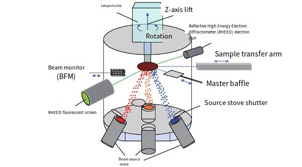
Molecular beam epitaxy (MBE) is a key technique for achieving atomic-level epitaxial growth under ultra-high vacuum (UHV, <10⁻⁶ Pa) conditions by precisely controlling atomic or molecular beams. As shown in Figure 1, it utilizes electron beam evaporators or Knudsen cells to regulate elemental fluxes, combined with reflection high-energy electron diffraction (RHEED) for real-time monitoring of surface reconstruction states, ensuring atomic-level precision during film growth. Researchers must first select a lattice-matched substrate and perform rigorous pre-treatment, including ultrasonic cleaning and high-temperature degassing to remove surface contaminants. Subsequently, ordered epitaxial growth is achieved by adjusting the flux ratios and substrate temperature. To optimize film quality, staged deposition strategies are often employed to suppress chamber outgassing, complemented by in-situ annealing processes to enhance crystallinity and electrical properties. Final film thickness can be precisely controlled to within ±1 monolayer error via growth rate and time [4].
In recent years, MBE technology has achieved several significant breakthroughs in preparing novel quantum materials, particularly superconductors. Qikun Xue et al. successfully prepared monolayer FeSe superconducting films on SrTiO₃ substrates with a critical temperature reaching 65 K by precisely controlling the Se/Fe flux ratio (2:1) and annealing process (450°C), setting a record for monolayer superconductors [5]. Hideo Hosono et al. utilized MBE to epitaxially grow high-quality films of the iron-based superconductor LaFeAsO on LaAlO₃ substrates, providing a key platform for in-depth study of its unconventional superconducting mechanism. Jia Li et al. precisely constructed superlattice structures of the heavy-fermion superconductor CeCoIn₅ using MBE, achieving atomic-scale control over its superconducting and magnetically ordered states and revealing the influence of dimensionality effects on superconductivity in strongly correlated electron systems [6]. These research achievements by leading teams fully demonstrate the unique advantages of MBE technology in precisely tuning material properties at the atomic scale, particularly for exploring and optimizing superconducting materials.
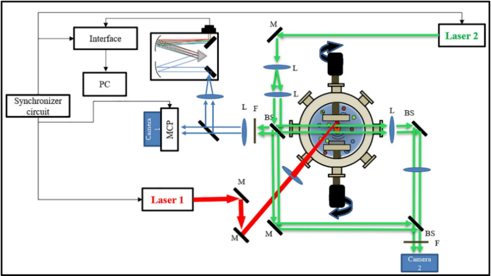
However, the slow growth rate and high equipment demands of MBE limit its application in large-area film fabrication. In contrast, pulsed laser deposition (PLD) is a technique based on ablating a target material with high-energy laser pulses to generate a plasma plume that deposits onto a substrate. Its core advantages are high deposition rates and the ability to maintain stoichiometry in complex oxide films. As shown in Figure 2, the operational procedure mainly involves placing the target and a pre-treated substrate in a vacuum chamber, ablating the target with a KrF excimer laser to excite a directional plasma plume towards the heated substrate. Precise control of film composition and thickness is achieved by regulating oxygen partial pressure, laser frequency, and deposition time.
PLD technology has recently demonstrated unique value in fabricating functional oxide films, particularly superconducting oxide films and heterostructures. V Moshnyaga et al. used PLD to successfully prepare YBCO / PBCO superconducting heterostructures with atomically flat interfaces on SrTiO₃ substrates. Through precise control of oxygen partial pressure and interface engineering, they significantly enhanced the critical current density of the YBCO layer under high magnetic fields. Harold Hwang et al. employed PLD combined with the TLAG process to epitaxially grow large-area Bi₂Sr₂CaCu₂O₈superconducting films on flexible mica substrates, laying the foundation for high-temperature superconducting flexible electronics [7]. Furthermore, Kui Jin et al. utilized their developed high-throughput combinatorial PLD technique to fabricate a library of hundreds of iron-based superconducting film samples with different compositions in parallel on a single SrTiO₃ substrate. Combined with rapid characterization methods, this significantly accelerated the exploration and optimization process for new high-temperature superconductors [8]. These advances highlight the immense technical potential of PLD for rapidly preparing high-performance superconducting films, exploring novel superconducting materials, and compatibility with novel substrates.
In summary, heteroepitaxial thin film growth techniques, through precise interface control and dimensionality tuning, provide important platforms for studying HTS mechanisms and developing novel superconducting materials. However, key challenges remain. Firstly, lattice matching constraints limit the choice of substrates and films; mismatches can lead to increased interfacial defects, degrading superconducting performance. Secondly, the thermodynamic instability of certain films (e.g., copper-based infinite-layer superconducting films) increases fabrication difficulty. Additionally, existing technologies still face limitations in achieving uniformity and reproducibility for large-area films. Nevertheless, with continuous advances in experimental techniques and theoretical simulations, the application prospects of this technology in superconducting electronics, energy transmission, and quantum computing remain broad.
3.2. Melt-Textured Growth (MTG)
Melt-textured growth (MTG) is a key technique for achieving directional crystal growth through precise control of temperature gradients and crystallization kinetics. Its core principle involves using directional solidification to reduce grain boundary defects and optimize material properties. The method prepares superconducting materials through three stages: raw material pre-treatment, directional crystallization, and post-processing. High-purity powders are calcined and ground, then encapsulated in an inert atmosphere or vacuum. Directional crystallization along specific orientations is induced using techniques like the vertical Bridgman method or top-seeded melt growth (TSMG). Finally, annealing is performed to eliminate defects. The entire process requires strict control of parameters such as temperature gradient, growth rate, and oxygen partial pressure to obtain highly oriented textured bulks or single crystals [9].
Significant progress has been made with MTG in the field of superconducting materials recently. Zhongxian Zhao et al. developed a novel MTG technique that successfully prepared large-sized Ba₀.₆K₀.₄Fe₂As₂ iron-based superconducting single crystals, revealing their intrinsic flux pinning mechanism. Additionally, Mina Aziziha, Athena S. Sefat et al. utilized a modified MTG technique (combining the top-seeded method) to successfully grow high-quality, centimeter-sized FeSe₁₋ₓTeₓ (x ≈ 0.5) single crystals. They systematically studied their superconducting properties and flux pinning behavior, providing an important platform for understanding the intrinsic properties of iron-based chalcogenide superconductors [10]. These advances underscore the critical role of MTG in preparing high-performance superconducting bulk materials and single crystals.
Despite its capability to produce high-performance superconducting materials, MTG faces numerous challenges. The method has extremely high equipment requirements; platinum crucibles and turbomolecular pumping systems contribute to high costs, and large single crystal growth cycles are long and inefficient. Simultaneously, stringent demands on raw material purity and thermal field uniformity further limit its industrial scalability. However, its advantages in suppressing weak-link behavior at grain boundaries and enhancing critical current density are irreplaceable, particularly demonstrated in the preparation of REBCO (Rare-Earth Barium Copper Oxide) and iron-based superconductors [11]. Future developments focusing on low-cost encapsulation technologies and automated growth monitoring systems hold promise for further advancing the application of this technique in the superconductivity field.
4. Characterization techniques
4.1. Morphological characterization
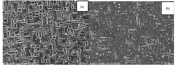
Scanning electron microscopy (SEM) constructs high-resolution three-dimensional topographic images by scanning a focused electron beam across the sample surface and detecting secondary electron and backscattered electron signals. Its large depth of field (up to millimeter scale) and nanometer-level resolution enable clear visualization of microstructures like surface roughness, cracks, and pores [12]. For non-conductive samples (e.g., polymers or oxides), a conductive coating (e.g., gold or platinum) is sputtered to mitigate charging effects, while energy-dispersive X-ray spectroscopy (EDS) enables micro-area elemental analysis. In SEM characterization of YBa₂Cu₃O₇₋δ (YBCO) superconducting films, the evolution of grains under different annealing temperatures can be observed. As shown in Figure 3, the film surface annealed at 700°C (a) shows uniformly distributed sub-micron grains with clear grain boundaries and porosity below 5%. In contrast, the sample annealed at 600°C (b) exhibits non-uniform grain size and localized aggregation of CuO impurity phases. EDS area mapping further verifies elemental distribution: the atomic ratio of Y, Ba, Cu is close to 1:2:3, but Cu enrichment occurs at grain boundaries, indicating that oxygen vacancy defects may cause local compositional deviation [13]. Furthermore, EDS line scans reveal a gradient change in oxygen content along the film thickness direction, directly related to oxygen diffusion kinetics during annealing. These data provide key evidence for optimizing oxygen annealing processes and enhancing superconducting critical current density. The advantage of SEM lies in its ability to rapidly acquire large-area morphological information while simultaneously performing compositional analysis, although electron beam irradiation can potentially damage sensitive samples.
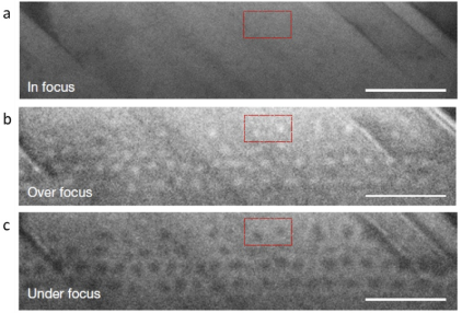
Transmission electron microscopy (TEM) utilizes a high-energy electron beam transmitted through an ultra-thin sample (<100 nm), generating high-resolution images from the intensity differences of transmitted and scattered electrons, achieving sub-Angstrom resolution (<0.1 nm) [14]. Jing Zhu et al. utilized TEM to report the first direct observation of topological magnetic vortex structures in pseudogap-state YBa₂Cu₃O₆.₅ material. Figure 4 a-c show Fresnel images of the pseudogap-state YBa₂Cu₃O₆.₅ sample under in-focus, over-focus, and under-focus conditions, respectively, with a defocus value of ±1.08 mm. The reversed contrast characteristics provide concrete evidence for the existence of topologically characteristic domain structures in this sample. The discovery of this topological magnetic vortex structure provides direct imaging evidence for time-reversal symmetry breaking in the pseudogap state at the real-space microscopic scale. Furthermore, it was found that this topological magnetic vortex structure is destroyed upon entering the charge density wave (CDW) state and reappears upon entering the superconducting state. This discovery is of great significance for revealing the microscopic mechanism of high-temperature superconductivity, and advanced transmission electron microscopy played an indispensable role in this finding [15].
4.2. Electrical characterization
The four-probe method is an electrical technique for precisely measuring the resistivity of materials. Its core principle involves using four independently arranged linear probes contacting the material surface: the outer two probes inject a constant current (I), while the inner two probes measure the resulting voltage drop (V) [16]. This separation of current and voltage probes effectively eliminates the influence of probe contact resistance and lead resistance on the measurement, making it particularly suitable for measuring low-resistance materials or thin film samples. In superconducting material characterization, the four-probe method plays a crucial role: Firstly, it determines the superconducting transition temperature. By measuring resistance as a function of temperature, the transition point from the normal state to the superconducting state is clearly observed, allowing to be determined. Secondly, it measures the critical current: At a constant temperature below and under an applied magnetic field, the current through the sample is gradually increased while monitoring voltage. When the current increases sufficiently to cause the superconductor to quench (exit the superconducting state), the voltage appears suddenly or rises sharply; the current at this point is the critical current. More importantly, the four-probe method also measures the critical magnetic field: At constant temperature, an external magnetic field is applied perpendicular or parallel to the current direction, and resistance is measured. When the field increases to the point where resistance recovers, the corresponding field is the critical magnetic field [17].
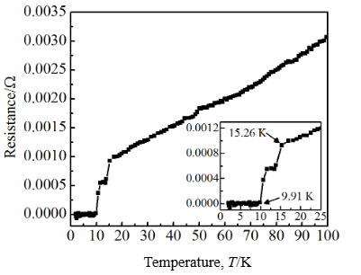
For instance, in studies of the superconducting properties of FeSe crystal materials, four-probe measurements showed a broad transition temperature range, with resistance dropping to zero at 9.91 K and an onset transition temperature of 15.26 K. As shown in Figure 5, the resistance (R) versus temperature (T) curve reveals metallic conductive behavior for FeSe crystals in the normal state. The sample begins to enter a broad transition region at 15.26 K and achieves zero-resistance superconductivity at 9.91 K, consistent with known results for FeSe crystals [18]. These parameters align with the typical characteristic values of FeSe crystals, fully confirming the superconducting properties of the crystal.
4.3. Optical characterization
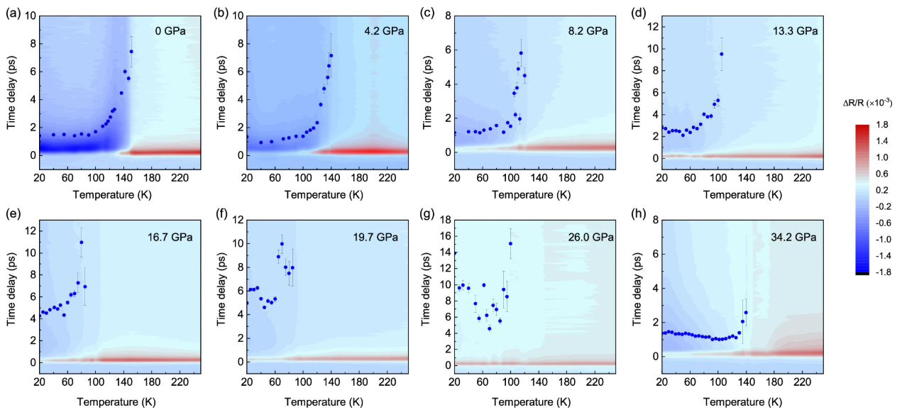
Pump-probe spectroscopy is an ultrafast laser-based time-resolved spectroscopic method that decouples the "excitation" and "probe" processes to observe the non-equilibrium dynamics of materials on atomic time scales. Its core principle is: First, a high-intensity pump pulse instantaneously excites the sample, driving the electron-phonon system out of equilibrium. Subsequently, a weak probe pulse with a controllable time delay (Δt) monitors the optical response of the sample. By scanning Δt and recording the evolution of the probe signal, the complete spatiotemporal evolution path of photoexcited carrier relaxation, order parameter fluctuations, and phase transition dynamics can be reconstructed. This technique is indispensable in superconductivity research: On one hand, its femtosecond time resolution can capture ultrafast processes like Cooper pair formation/dissociation and phonon bottleneck effects. On the other hand, by analyzing transient spectral features, microscopic parameters such as superconducting gap dynamics and electron-boson coupling strength can be inferred. Especially under extreme conditions, its non-contact measurement capability provides a crucial experimental window for frontier issues like near-room-temperature hydride superconductivity and the strange metal phase in cuprates [19]. For example, Meng Wang et al. demonstrated the groundbreaking application of pump-probe spectroscopy in resolving complex superconducting phase transition mechanisms. Their study focused on the novel bilayer nickelate superconductor La₃Ni₂O₇ under high pressure, constructing the world's first dynamic "Pressure-Density Wave Order-Superconductivity" phase diagram. As shown in Figure 6, the team utilized a self-developed high-pressure ultrafast pump-probe system. By precisely measuring the relaxation dynamics and spectral characteristics of transient reflectivity changes (ΔR/R) at different pressures, they provided a paradigm case for understanding the superconducting mechanism in layered oxides [20].
5. Conclusions and outlook
Current preparation and characterization techniques for superconducting materials have achieved significant breakthroughs. Heteroepitaxial techniques enable the controllable preparation of high-performance thin films like monolayer FeSe through atomic-level interface control. Melt-textured growth (MTG) effectively suppresses weak-link behavior at grain boundaries via directional solidification, significantly enhancing the critical current density of REBCO and iron-based superconductors. In the characterization domain, atomic-resolution TEM revealed topological magnetic vortex structures in the pseudogap state for the first time. Femtosecond pump-probe spectroscopy successfully resolved the non-equilibrium dynamics of high-pressure nickelate superconductors, providing key experimental support for mechanism studies. However, technological bottlenecks still constrain practical applications: MBE equipment is costly and slow; PLD faces challenges in achieving uniformity for large-area films; MTG relies on expensive equipment like platinum crucibles, hindering scalability. In-situ characterization under extreme conditions suffers from limited precision, and electron beam irradiation can easily damage sensitive samples.
To address these challenges, future efforts need to focus on two major directions for breakthroughs: The practical realization of room-temperature superconductivity requires overcoming the high-pressure limitation – while the achievement of superconductivity at 287.7 K in carbonaceous sulfur hydride under 267 GPa pressure confirms feasibility, exploring ambient-pressure stabilization pathways through interface engineering or chemical doping is essential, coupled with high-throughput techniques to accelerate new material screening. Deep integration of artificial intelligence will revolutionize research paradigms. For instance, machine learning can be used to analyze SEM/TEM image libraries for automatic defect recognition to optimize processes; generative adversarial networks (GANs) can design novel hydride structures; or intelligent control systems can regulate MBE flux ratios and PLD oxygen partial pressures to enhance reproducibility. Driven by advancements in fabrication techniques and discoveries of novel superconducting systems, the application scope of superconducting materials has expanded beyond traditional high-power domains to emerging frontiers including quantum information and sustainable energy systems, demonstrating a clear trend toward interdisciplinary integration [21].
In the field of quantum computing, superconducting qubits have emerged as the predominant technological approach. Superconducting circuits based on aluminum or niobium (Nb), utilizing Josephson junctions for quantum state manipulation, have seen their coherence times advance from the initial nanoseconds to the order of hundreds of microseconds. For instance, IBM's "Osprey" processor integrates 433 superconducting qubits and has achieved a logical qubit error rate below 10⁻³ through error correction coding. The "Zuchongzhi" prototype developed by Pan Jianwei et al. demonstrated "quantum computational advantage" using superconducting circuits, performing random circuit sampling tasks 100 million times faster than classical supercomputers.Even more noteworthy is the progress in topological quantum computing [22]. The discovery of Majorana zero modes in the iron-based superconductor FeTe₀.₅Se₀.₅ offers a potential pathway for creating non-Abelian anyons. Jia Jinfeng et al. observed chiral transport signatures of Majorana bound states on the surface of FeTe₀.₅Se₀.₅ single crystals via molecular beam epitaxy (MBE), providing crucial experimental groundwork for the physical realization of topological qubits. Additionally, superconducting nanowire single-photon detectors (SNSPDs) play a pivotal role in quantum communication.
In the energy sector, superconducting technology is driving innovations in power transmission and storage. The 1.2-km MgB₂ superconducting DC cable deployed by Korea Electric Power Corporation (KEPCO), operating at 20 K, delivers a transmission capacity of 500 MW. It exhibits losses only one-tenth of conventional copper cables while using 90% less conductor material. The European "SuperNode" initiative aims to deploy a YBCO-tape-based superconducting power grid by 2030, targeting renewable energy grid integration efficiency exceeding 99% [23].Nuclear fusion energy represents another critical arena for superconducting materials. The International Thermonuclear Experimental Reactor (ITER) employs Nb₃Sn superconducting magnets to generate a 23 T magnetic field for plasma confinement. China's CFETR (China Fusion Engineering Test Reactor) goes further, testing magnet systems based on second-generation high-temperature superconducting (HTS) REBCO tapes. REBCO maintains a critical current density exceeding 1 MA/cm² even at the liquid nitrogen temperature of 77 K, enabling fusion devices to eliminate reliance on liquid helium cooling and significantly reduce operational costs. The SPARC device, developed by US-based Commonwealth Fusion Systems and slated for Q>1 achievement by 2025, centers around a compact tokamak built with HTS magnets.The integration of superconductivity with other quantum materials has spawned numerous novel phenomena. For example, the potential topological superconducting states in superconductor-topological insulator heterostructures offer new platforms for controlling Majorana fermions [24]. In smart materials research, artificial intelligence is accelerating the discovery and optimization of superconducting materials. DeepMind's generative model "SuperConX," by analyzing databases containing millions of crystal structures, predicted 12 potential room-temperature superconductors, three of which have exhibited superconducting transitions in high-pressure experiments [25].
Looking ahead, with advancements in materials genomics and extreme-condition characterization techniques, superconducting materials hold the promise of catalyzing a new wave of technological revolutions in areas such as the quantum internet, lossless power grids, and fusion energy.
References
[1]. CHRIEFFER J R. Theory of superconductivity [M]. CRC press, 2018.
[2]. ZHOU X, LEE W-S, IMADA M, et al. High-temperature superconductivity [J]. Nature Reviews Physics, 2021, 3(7): 462-5.
[3]. KOMNIK A, THORWART M. BCS theory of driven superconductivity [J]. The European Physical Journal B, 2016, 89(11): 244.
[4]. HORIKOSHI Y. General description of MBE [J]. Molecular Beam Epitaxy: Materials and Applications for Electronics and Optoelectronics Wiley, 2019: 23-39.
[5]. XU H-S, XIE W. Synthesis methods, basic physical properties, and potential applications of the FeSe superconductor [J]. Coordination Chemistry Reviews, 2024, 501: 215591.
[6]. VAN DYKE J S, MASSEE F, ALLAN M P, et al. Direct evidence for a magnetic f-electron–mediated pairing mechanism of heavy-fermion superconductivity in CeCoIn5 [J]. Proceedings of the National Academy of Sciences, 2014, 111(32): 11663-7.
[7]. LI D, LEE K, WANG B Y, et al. Superconductivity in an infinite-layer nickelate [J]. Nature, 2019, 572(7771): 624-7.
[8]. WALLER G H. Template Directed Growth of Nb doped SrTiO₃ using Pulsed Laser Deposition [D]; Virginia Tech, 2011.
[9]. HE J, WANG Y, LI W, et al. Effects of Zn doping on superconducting properties of melt textured Y–Ba–Cu–O bulk superconductors [J]. Superconductor Science and Technology, 2022, 35(7): 074005.
[10]. JIANG X, QIN M, WEI X, et al. Interplay between superconductivity and the strange-metal state in FeSe [J]. Nature Physics, 2023, 19(3): 365-71.
[11]. DOGRUER M, MOTOKI T, SEMBA M, et al. Mechanical properties of Ag-added DyBa2Cu3Oy superconducting melt-textured bulks prepared by the single-direction melt growth method [J]. Materials Today Communications, 2024, 39: 108605.
[12]. GRüNEWALD L, NERZ D, LANGER M, et al. Analysis of superconducting thin films in a modern FIB/SEM dual-beam instrument [J]. Microscopy and Microanalysis, 2021, 27(S1): 1056-8.
[13]. HUSSEIN A A, HUSSEIN A A, HASAN N A. Study of the properties of YBCO superconductor compound in various preparation methods: a short review [J]. Journal of Applied Sciences and Nanotechnology, 2023, 3(1): 65-79.
[14]. WANG Z, PEI K, YANG L, et al. Topological spin texture in the pseudogap phase of a high-T c superconductor [J]. Nature, 2023, 615(7952): 405-10.
[15]. MOHSIN A, AL-SHAKARCHI E K. The Conductivity Parameters of YBa2Cu3O6. 5+ Superconductor Compound [J]. Al-Nahrain Journal of Science, 2022, 25(1): 24-9.
[16]. EREMETS M I. The current status and future development of high-temperature conventional superconductivity [J]. National Science Review, 2024, 11(7): nwae047.
[17]. POLáČKOVá M, ZHITLUKHINA E, BELOGOLOVSKII M, et al. Probing superconducting granularity using nonlocal four-probe measurements [J]. The European Physical Journal Plus, 2023, 138(6): 1-8.
[18]. HU S, XUE J, WANG X, et al. Evidence for nematic fluctuations in FeSe superconductor: a 57Fe Mössbauer spectroscopy study [J]. Journal of Physics: Condensed Matter, 2024, 37(3): 035402.
[19]. BLOMMEL T, KAYE J, MURAKAMI Y, et al. Chirped amplitude mode in photoexcited superconductors [J]. Physical Review B, 2025, 111(9): 094502.
[20]. MENG Y, YANG Y, SUN H, et al. Density-wave-like gap evolution in La3Ni2O7 under high pressure revealed by ultrafast optical spectroscopy [J]. Nature Communications, 2024, 15(1): 10408.
[21]. HUANG H-L, WU D, FAN D, et al. Superconducting quantum computing: a review [J]. Science China Information Sciences, 2020, 63(8): 180501.
[22]. GAMBETTA J M, CHOW J M, STEFFEN M. Building logical qubits in a superconducting quantum computing system [J]. npj quantum information, 2017, 3(1): 2.
[23]. BRAVYI S, DIAL O, GAMBETTA J M, et al. The future of quantum computing with superconducting qubits [J]. Journal of Applied Physics, 2022, 132(16).
[24]. ADETOKUN B B, OGHORADA O, ABUBAKAR S J A. Superconducting magnetic energy storage systems: Prospects and challenges for renewable energy applications [J]. Journal of Energy Storage, 2022, 55: 105663.
[25]. PAPAGEORGIOU P G, OUREILIDIS K O, CHRISTOFORIDIS G C. A systematic review of hybrid superconducting magnetic/battery energy storage systems: Applications, control strategies, benefits, limitations and future prospects [J]. Renewable and Sustainable Energy Reviews, 2023, 183: 113436.
Cite this article
Wang,X. (2025). Preparation and Advanced Characterization Techniques for Novel Superconducting Materials. Applied and Computational Engineering,186,177-188.
Data availability
The datasets used and/or analyzed during the current study will be available from the authors upon reasonable request.
Disclaimer/Publisher's Note
The statements, opinions and data contained in all publications are solely those of the individual author(s) and contributor(s) and not of EWA Publishing and/or the editor(s). EWA Publishing and/or the editor(s) disclaim responsibility for any injury to people or property resulting from any ideas, methods, instructions or products referred to in the content.
About volume
Volume title: Proceedings of CONF-FMCE 2025 Symposium: Semantic Communication for Media Compression and Transmission
© 2024 by the author(s). Licensee EWA Publishing, Oxford, UK. This article is an open access article distributed under the terms and
conditions of the Creative Commons Attribution (CC BY) license. Authors who
publish this series agree to the following terms:
1. Authors retain copyright and grant the series right of first publication with the work simultaneously licensed under a Creative Commons
Attribution License that allows others to share the work with an acknowledgment of the work's authorship and initial publication in this
series.
2. Authors are able to enter into separate, additional contractual arrangements for the non-exclusive distribution of the series's published
version of the work (e.g., post it to an institutional repository or publish it in a book), with an acknowledgment of its initial
publication in this series.
3. Authors are permitted and encouraged to post their work online (e.g., in institutional repositories or on their website) prior to and
during the submission process, as it can lead to productive exchanges, as well as earlier and greater citation of published work (See
Open access policy for details).
References
[1]. CHRIEFFER J R. Theory of superconductivity [M]. CRC press, 2018.
[2]. ZHOU X, LEE W-S, IMADA M, et al. High-temperature superconductivity [J]. Nature Reviews Physics, 2021, 3(7): 462-5.
[3]. KOMNIK A, THORWART M. BCS theory of driven superconductivity [J]. The European Physical Journal B, 2016, 89(11): 244.
[4]. HORIKOSHI Y. General description of MBE [J]. Molecular Beam Epitaxy: Materials and Applications for Electronics and Optoelectronics Wiley, 2019: 23-39.
[5]. XU H-S, XIE W. Synthesis methods, basic physical properties, and potential applications of the FeSe superconductor [J]. Coordination Chemistry Reviews, 2024, 501: 215591.
[6]. VAN DYKE J S, MASSEE F, ALLAN M P, et al. Direct evidence for a magnetic f-electron–mediated pairing mechanism of heavy-fermion superconductivity in CeCoIn5 [J]. Proceedings of the National Academy of Sciences, 2014, 111(32): 11663-7.
[7]. LI D, LEE K, WANG B Y, et al. Superconductivity in an infinite-layer nickelate [J]. Nature, 2019, 572(7771): 624-7.
[8]. WALLER G H. Template Directed Growth of Nb doped SrTiO₃ using Pulsed Laser Deposition [D]; Virginia Tech, 2011.
[9]. HE J, WANG Y, LI W, et al. Effects of Zn doping on superconducting properties of melt textured Y–Ba–Cu–O bulk superconductors [J]. Superconductor Science and Technology, 2022, 35(7): 074005.
[10]. JIANG X, QIN M, WEI X, et al. Interplay between superconductivity and the strange-metal state in FeSe [J]. Nature Physics, 2023, 19(3): 365-71.
[11]. DOGRUER M, MOTOKI T, SEMBA M, et al. Mechanical properties of Ag-added DyBa2Cu3Oy superconducting melt-textured bulks prepared by the single-direction melt growth method [J]. Materials Today Communications, 2024, 39: 108605.
[12]. GRüNEWALD L, NERZ D, LANGER M, et al. Analysis of superconducting thin films in a modern FIB/SEM dual-beam instrument [J]. Microscopy and Microanalysis, 2021, 27(S1): 1056-8.
[13]. HUSSEIN A A, HUSSEIN A A, HASAN N A. Study of the properties of YBCO superconductor compound in various preparation methods: a short review [J]. Journal of Applied Sciences and Nanotechnology, 2023, 3(1): 65-79.
[14]. WANG Z, PEI K, YANG L, et al. Topological spin texture in the pseudogap phase of a high-T c superconductor [J]. Nature, 2023, 615(7952): 405-10.
[15]. MOHSIN A, AL-SHAKARCHI E K. The Conductivity Parameters of YBa2Cu3O6. 5+ Superconductor Compound [J]. Al-Nahrain Journal of Science, 2022, 25(1): 24-9.
[16]. EREMETS M I. The current status and future development of high-temperature conventional superconductivity [J]. National Science Review, 2024, 11(7): nwae047.
[17]. POLáČKOVá M, ZHITLUKHINA E, BELOGOLOVSKII M, et al. Probing superconducting granularity using nonlocal four-probe measurements [J]. The European Physical Journal Plus, 2023, 138(6): 1-8.
[18]. HU S, XUE J, WANG X, et al. Evidence for nematic fluctuations in FeSe superconductor: a 57Fe Mössbauer spectroscopy study [J]. Journal of Physics: Condensed Matter, 2024, 37(3): 035402.
[19]. BLOMMEL T, KAYE J, MURAKAMI Y, et al. Chirped amplitude mode in photoexcited superconductors [J]. Physical Review B, 2025, 111(9): 094502.
[20]. MENG Y, YANG Y, SUN H, et al. Density-wave-like gap evolution in La3Ni2O7 under high pressure revealed by ultrafast optical spectroscopy [J]. Nature Communications, 2024, 15(1): 10408.
[21]. HUANG H-L, WU D, FAN D, et al. Superconducting quantum computing: a review [J]. Science China Information Sciences, 2020, 63(8): 180501.
[22]. GAMBETTA J M, CHOW J M, STEFFEN M. Building logical qubits in a superconducting quantum computing system [J]. npj quantum information, 2017, 3(1): 2.
[23]. BRAVYI S, DIAL O, GAMBETTA J M, et al. The future of quantum computing with superconducting qubits [J]. Journal of Applied Physics, 2022, 132(16).
[24]. ADETOKUN B B, OGHORADA O, ABUBAKAR S J A. Superconducting magnetic energy storage systems: Prospects and challenges for renewable energy applications [J]. Journal of Energy Storage, 2022, 55: 105663.
[25]. PAPAGEORGIOU P G, OUREILIDIS K O, CHRISTOFORIDIS G C. A systematic review of hybrid superconducting magnetic/battery energy storage systems: Applications, control strategies, benefits, limitations and future prospects [J]. Renewable and Sustainable Energy Reviews, 2023, 183: 113436.