


1. Introduction
FIFO (First in First Out) or First in First Out queue. An asynchronous FIFO acts as a buffer between two different clock domains to resolve timing differences due to inter-clock domain transfers. A traditional asynchronous FIFO circuit includes data storage, pointer synchronization, and empty-full detection modules, and the schematic block diagram is shown in Figure 1. The data storage module absorbs the time differences between the write clock domain and the read clock domain. The pointer synchronization module synchronizes the pointer signals to another clock domain. An empty-full detection module detects and provides feedback whether the FIFO is empty or full [1].
2. Analysis of the basic principles and improvements of the fifo (structure, working principle)
2.1. Fundamentals
2.1.1. Structure. There are two basic structures for monolithic FIFOs: trigger-oriented structures and zero-oriented transfer structures. A trigger-oriented transfer structure FIFO consists of an array of registers, while a zero-directional transfer structure FIFO consists of a dual-ported RAM with read and write address pointers.
A FIFO used in FPGAs generally refers to a cache with a first-in-first-out feature for data storage and is often used for high-speed asynchronous data communication known as data caching or clock-to-clock. It differs from RAM and ROM inside an FPGA in that there are no external read/write address lines and data is written sequentially and read sequentially, making it simple and easy to use.
FIFOs can be divided into synchronous FIFOs and asynchronous FIFOs according to the time domain in which the FIFO operates. synchronous FIFOs are clocks where the read and write clocks are the same, and when a clock edge occurs, read and write operations occur simultaneously. The Xilinx FIFO IP core can be configured as either a synchronous FIFO or an asynchronous FIFO. When configured as a synchronous FIFO, only wr_clk is used and all input and output signals are synchronized with the wr_clk signal. When configured as an asynchronous FIFO.
2.1.2. Working principle. A typical synchronous FIFO consists of three parts: FIFO write control logic, FIFO read control logic, and FIFO storage objects.
The main function of FIFO writes control logic: generate FIFO write address, write valid signal, FIFO full write, write error and other status signals; The main function of FIFO read control logic: Generate FIFO read address, read valid signal, FIFO read empty, read error and other status signals.
When the FIFO is reset, fifo_write_addr and fifo_read_addr point to the same 0x0, when the FIFO is empty; When the FIFO performs a write operation, fifo_write_addr is incremented (rolled back when the FIFO reaches DEPTH) and incremented by fifo_read_addr, at which point the FIFO is in a non-empty state; fifo_read_addr is incremented when performing a FIFO read operation.
In hardware terms, a FIFO is a piece of data memory. It has 2 ports, one for writing data i.e. putting data into the FIFO and one for reading data i.e. removing data from the FIFO. The FIFO controller controls the movement of these two pointers through external read and write signals that generate the FIFO empty or full signals. [2] A Count counter is implemented to indicate the number of data stored within the FIFO to generate the FIFO empty and full flags; if there is only a write operation, Count is incremented by 1; if there is a read-only operation, Count is subtracted from 1; in other cases it remains unchanged; When Count is 0, it means that the FIFO is empty and fifo_empty is set; When Count is equal to FIFO_ DEPTH, it means that the FIFO is empty. DEPTH, FIFO is full and fifo_full is set.
2.2. Analysis of improvement methods
For synchronous FIFO designs, an application counts the number of rights to the FIFO buffer and reads from this FIFO buffer until the increment (the FIFO is written but not read at time), the current fill value of the FIFO buffer decrement (FIFO read but not written) or hold (when there are no write and read or simultaneous write and read operations). The FIFO is full when the FIFO counter reaches a predetermined integer value, and empty when the FIFO counter is zero.
Unfortunately, for asynchronous FIFO designs, it is not possible to fill the counter with an incrementally decreasing FIFO because two different asynchronous clocks are required to drive the counter. To determine the full and empty states of an asynchronous FIFO design, the write pointer and the read pointer must be compared.
One way to solve this problem is to select and store a periodic binary count value in a hold register and transfer the synchronous ready signal to the new clock domain. When a ready signal is recognized, the receiving clock domain sends a synchronization acknowledgment signal back to the transmitting clock domain. The sample pointer shall not change until an acknowledgment signal is received from the receive clock domain. Using this technique, count values with multiple shift bits can be safely transferred to a new clock domain. After the acknowledgment signal is received, the transmit clock field allows the ready signal to be cleared and the binary count value to be resampled.
With this technique, binary counter values are sampled periodically and not all binary counter values can be transferred to the new clock field. The question is, should we be concerned that binary counters might keep incrementing the FIFO between sampled counter values and overflowing or overflowing? The answer is no.
When the write pointer catches up with the synchronous and sample read pointers, the FIFO will be full. Synchronous and sampled read pointers may not reflect the current value of the actual read pointer, but the write pointer will not attempt to count over the synchronous read pointer value. No flooding will occur.
Since the control of the read/write flag operates in different clock domains in its generation cycle, when the comparative trigger setup time and hold time requirements are not met, the trigger goes to an intermediate state between logic 1 and logic 0, which is called sub-stable. To reduce the possibility of substability, Gray coded address calculation can be used [3]. If a pointer is sampled and a handshaking control signal is used to securely transfer a sampled binary count value between the two clock domains, then a binary pointer can be used for FIFO design. Each synchronous Gray Code indicator requires 2n triggers (2 for each indicator bit). Sampled multi-bit registers require 2n+4 triggers (1 for each storage register bit in each clock domain, 2 triggers for synchronous ready bits, and 2 triggers for synchronous acknowledge bits). There is no significant difference in the probability of sub-stable state of both indicator styles. Using binary pointers, it is easy to use simple binary operations between pointer values to calculate the "almost empty" and "almost full" status bits.
3. Relevant application analysis
3.1. Ping-pong mode high-speed data acquisition system
Compared with traditional electrical sensors, fiber optic grating sensors have high sensitivity, small size, corrosion resistance, anti-electromagnetic interference and other advantages [4, 5], designed a high-speed data acquisition system based on STM32 and asynchronous FIFO. The system uses STM32 as the core and TIADC structure to realize two-channel alternate sampling to improve the sampling speed of the system; Two asynchronous FIFOs are used in each channel to realize table tennis caching technology, which completes high-speed storage and real-time processing of signal data and transmits data to the main computer via WIFI communication. [6]
Figure 1. Block diagram of the overall system solution.
After data acquisition, the incoming analog signal is passed through the signal conditioning module to generate two differential signals, which are alternately selected by the dual-channel ADC in the data acquisition and cache module to complete the conversion of the analog signal to a digital signal. To increase the sampling rate, the TIADC structure is used for analog-to-digital conversion, which is an efficient way to achieve high-speed and high-precision analog-to-digital conversion based on time-varying parallel analog. -digital converter sampling structure and therefore widely used in high-speed data acquisition systems.
Data acquisition and transmission are performed simultaneously, digital signals generated by analog-to-digital conversion are cached in two asynchronous FIFOs on their respective channels. In the first cycle, data is stored in "Asynchronous FIFO 0" memory; in the second cycle, data is stored in "Asynchronous FIFO 1" memory; and so on. Until the FIFO is full and sampling is stopped and the data in the asynchronous FIFO is fed to the data processing module. The data in the asynchronous FIFO is fed to the data processing module, and sampling continues after the transfer is complete. By clocking and cycling asynchronous FIFOs throughout the process, data is continuously processed and seamlessly cached and retrieved.
Data processing and system synchronization are performed by the STM32 master control chip [7], which controls the clock signal module to generate clock signals of different frequencies, ensuring the synchronous operation of the electronics of the high-speed data acquisition system. The final connection to the host computer is via the WIFI module, which transmits the sampled data to the host computer for display.
The role of the signal conditioning module in this system design is to process the input analog signal and provide a stable, high signal-to-noise ratio differential input signal for the analog-to-digital converter module. Compared to single-ended inputs, differential inputs are more stable, less prone to corrupted code, and have the ability to suppress electromagnetic interference and perform basic signal conditioning. Considering the power and noise levels, the ADI ADA4932 was chosen for this module, which offers a significant increase in performance by integrating the functionality of a large number of discrete devices, achieving a significant reduction in noise and power consumption, thus helping engineers simplify. their design tasks while saving space on the board. Like single-ended-differential amplifier or differential-differential.
The ADA4932 is a high-performance amplifier and is ideal for driving high-performance ADCs. Adjusting the differential output voltage and common-mode bias to match the input voltage range of the analog-to-digital converter is achieved by calculating and adjusting the value of the feedback resistance of the ADA4932 to adjust the closed-loop gain of the amplifier [8].
The analog-to-digital converter module is used to convert analog signals to digital signals, and the module is based on the MXT2088, an 8-bit, low-power, high dynamic range, fully differential input ADC with a maximum sampling rate of 100. Example/s. It has two internal ADC channels, each of which can be independently driven by phase clock signals (CLK-ADC0, CLK-ADC1) of different frequencies. Each channel can be independently driven by a different frequency phase clock signal (CLK-ADC0, CLK-ADC1) corresponding to the TIADC architecture used in this design. With a sampling rate of 100 Msps, the chip has a 66-dbc spurious dynamic range (SFDR) and a 44-dB signal-to-noise ratio (SNR), achieving 475 MHz analog input bandwidth for system response. requirements. The data acquisition system uses a parallel data interface for communication to provide the transfer rate to and from the STM32H750VBT6 main control chip.
The main function of the data buffer module is to match the input speed of the data acquisition module with the data processing speed. Using an asynchronous FIFO as a data transfer buffer is a simple and effective way to solve the speed matching problem. As shown in Figure 2, the front end of the module uses a 74LVC574 D flip-flop model to latch the output data of the ADC chip to the next asynchronous FIFO after a maximum delay of 7 ns. CLK-D0 and CLK-D1 are the control D flip-flop clock signals.
Figure 2. Data cache module D flip-flop circuit.
The lower computer mainly completes the clock synchronization of the control system, real-time data acquisition, data processing and communication with the upper computer, while the upper computer mainly completes the real-time display of the waveform data transmitted by the lower computer, as shown below. Figure 3.
Figure 3. General structure of the software section.
A Gaussian pulse signal with a pulse width of 140 ns and an amplitude of 2 V was generated by the signal generator to test the sampling performance of the high-speed data acquisition system for the reflection waveform of the optical fiber grating. optical fiber grating reflectance spectrum. As can be seen from Figure 4, the high-speed data acquisition system can sample the Gaussian curve signal, thus verifying that the sampling system is capable of collecting the reflection spectrum of the optical fiber grating. The system has been tested several times and is stable, showing clear waveforms without any serious distortion and meeting design specifications. The test proves that the data sampling system achieves high-speed data acquisition with low power consumption, 16 K storage depth, and 200 Msample/s maximum sampling rate, which can meet the engineering needs of the power industry.
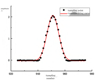
Figure 4. Gaussian fitted curve of the simulated reflection spectrum.
3.2. Colour sorter sorting system
The main function of the sorting system of the color sorter is to collect and process the detection signal output from the detection system and output the sorting pulse signal with a certain delay and width for the sorting solenoid valve. In a multichannel sorter, each channel signal is completely uncorrelated and completely random, typically using completely independent and separate processing techniques that require processing and delay for each signal of each channel [9]. Considering the control requirements of the multi-channel color sorter system, high signal control accuracy and high real-time performance, the communication, control and driver hardware circuit of the sorter system is designed with a high-speed parallel FPGA as control. a basic, accurate and lossless control strategy for the signal is proposed, the implementation of each subroutine module of the sorter system is given, and the performance of the sorter system is verified using simulation and experimental platforms. The human-machine interface exchanges data with the sorting system via RS485 bus to achieve real-time adjustment and communication of sorting parameters; the detection system transmits the detection signals to the sorting system via a serial communication bus; The FPGA is selected as the control core of the sorting system to complete the serial and parallel conversion of detection signals and accurate destructive delay and sorting pulse signal. The UART (Universal Asynchronous Receiver Transmitter) interface module implements and communicates with the UART [10].
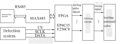
Figure 5. Block diagram of the sorting system.
The signal generation circuit mainly uses EP4C15F256C8 FPGA chip to achieve detection signal delay and pulse signal generation. The chip has 504K of internal RAM, more than 15,000 LEs, 4 PLL phase-locked circuits, and 165 I/O ports, 53 of which have differential input functions that can meet the performance requirements of this control system. The driver circuit uses multiple half-bridge driver chips DRV8844PWP to control the sorting solenoid valves, each driver chip can control 4 solenoid valves. As can be seen from Figure 5.
CLK is the clock signal, the FIFO control module generates the FIFO write enable signal WR and the read enable signal RD on the rising edge of each clock, the write enable signal writes the D0 data to the FIFO while reading the Dn-1 data. FIFO Since FIFO is first-in-first-out, the data delay time after FIFO is: Td = TCLK x n (1) Eq: TCLK is the cycle of the CLK clock signal; n is the number of CLK clocks that the read enable signal RD lags behind the write enable signal WR. Let k be the number of channels of the sorting system, each channel corresponds to one bit of data, the k channel of the detection signal consists of k-bit data, so the internal RAM of the FPGA is configured to k-bit. synchronous FIFO width. This prevents the continuous loss of abnormal material signals in processor-based sorting systems.
The sort pulse generation module will output the sort pulse signal for each sort solenoid valve according to the delay signal and the set operation time of each channel. Depending on the size of the material to be sorted and its speed through the sorting solenoid valve nozzles, the operating time Tw of the sorting solenoid valve is different and is set by the HMI. Inside the FPGA, a monostable counter is developed for each channel of the solenoid valve travel time, it starts counting on the rising edge of the delay signal and gives the sort signal, and stops counting when the count reaches the specified operation time and turns off the device. sorting signal. Using the parallel execution of FPGA software, the counters of each channel work individually, are accurately calculated, and can meet the requirements of each channel's solenoid valve control.
In summary, considering the control requirements of multi-channel, high signal control accuracy and high real-time color sorting system, the communication, control and control hardware circuit of the sorting system is designed with high-speed parallel FPGA. a control kernel and an accurate and lossless signal control strategy are proposed, after which the performance of the sorting system is verified using a simulation and experimental platform.
4. Conclusion
The article analyzes the structure and working principle of FIFO in the use of Gray code to solve the heterogeneous problem. The sub-steady-state problem in the step system proposed the use of a binary pointer optimization method, and also presented a high-speed data acquisition system based on STM32 and an asynchronous FIFO designed for the power industry. In addition to the low delay accuracy of the color sorting signal, the problem of signal loss designed for the control core of the color sorting machine's sorting system is of great importance to improve the detection level and productivity of the color sorting machine.
References
[1]. Chen, W., Liu, W., Zhang, F., & Hou, Y. (2021). An Embedded High-Speed Data Acquisition System Based on the Asynchronous FIFO. Sensors, 21(13), 4350. https://doi.org/10.3390/s21134350
[2]. Zhu, X., Yang, J., Wang, C., & Jiang, Z. (2019). Research on the optimization of the asynchronous FIFO for high-speed communication system. In 2019 IEEE International Conference on Mechatronics and Automation (ICMA) (pp. 230-235). IEEE. https://doi.org/10.1109/ICMA.2019.8812299
[3]. Li, M., Chen, Y., & Li, Z. (2017). Improved Asynchronous FIFO Design and Implementation for Efficient Data Communication. Journal of Circuits, Systems and Computers, 26(8), 1650163. https://doi.org/10.1142/S0218126616501634
[4]. Ma, L., & Hu, J. (2021). A New FIFO Model Based on Dynamic Storage Allocation. Journal of Physics: Conference Series, 1841(1), 012120. https://doi.org/10.1088/1742-6596/1841/1/012120
[5]. Zhang, Y., & Yang, K. (2019). The Design of an Asynchronous FIFO Buffer with Binary Pointers. Advances in Computer Science Research, 94, 27-30. https://doi.org/10.2991/arsi-19.2019.6
[6]. Shi, L., & Wu, S. (2018). An Efficient Write-Optimized FIFO Design for High-Speed Data Acquisition System. International Journal of Electronics, 105(8), 1386-1401. https://doi.org/10.1080/00207217.2018.1496059
[7]. Li, Y., Li, Y., Wei, F., & Li, F. (2016). An Optimized Design of Asynchronous FIFO for High-Speed Data Acquisition Based on DSP. Journal of Computational and Theoretical Nanoscience, 13(5), 3720-3729. https://doi.org/10.1166/jctn.2016.5091
[8]. Liu, S., Yue, Y., Yang, M., & Li, Q. (2020). A Novel Architecture of Asynchronous FIFO Buffer Based on Binary Pointers. Journal of Physics: Conference Series, 1578(3), 032023. https://doi.org/10.1088/1742-6596/1578/3/032023
[9]. Xiong, Z., Wang, H., Zhang, W., & Cai, J. (2021). A high-throughput FIFO design utilizing adaptive pointer selection algorithm. Microelectronics Journal, 117, 105128. https://doi.org/10.1016/j.mejo.2021.105128
[10]. Sun, Z., Zhao, L., Fan, Y., & Liu, Y. (2016). A High-Performance Dynamic-FIFO System Design Based on FPGA. Advances in Science and Technology of Water Resources, 36(4), 25-30. https://doi.org/10.13651/j.cnki.slxb.2016.04.006
Cite this article
Luo,R. (2023). Introduction and application analysis of FIFO-related methods. Applied and Computational Engineering,14,103-110.
Data availability
The datasets used and/or analyzed during the current study will be available from the authors upon reasonable request.
Disclaimer/Publisher's Note
The statements, opinions and data contained in all publications are solely those of the individual author(s) and contributor(s) and not of EWA Publishing and/or the editor(s). EWA Publishing and/or the editor(s) disclaim responsibility for any injury to people or property resulting from any ideas, methods, instructions or products referred to in the content.
About volume
Volume title: Proceedings of the 5th International Conference on Computing and Data Science
© 2024 by the author(s). Licensee EWA Publishing, Oxford, UK. This article is an open access article distributed under the terms and
conditions of the Creative Commons Attribution (CC BY) license. Authors who
publish this series agree to the following terms:
1. Authors retain copyright and grant the series right of first publication with the work simultaneously licensed under a Creative Commons
Attribution License that allows others to share the work with an acknowledgment of the work's authorship and initial publication in this
series.
2. Authors are able to enter into separate, additional contractual arrangements for the non-exclusive distribution of the series's published
version of the work (e.g., post it to an institutional repository or publish it in a book), with an acknowledgment of its initial
publication in this series.
3. Authors are permitted and encouraged to post their work online (e.g., in institutional repositories or on their website) prior to and
during the submission process, as it can lead to productive exchanges, as well as earlier and greater citation of published work (See
Open access policy for details).
References
[1]. Chen, W., Liu, W., Zhang, F., & Hou, Y. (2021). An Embedded High-Speed Data Acquisition System Based on the Asynchronous FIFO. Sensors, 21(13), 4350. https://doi.org/10.3390/s21134350
[2]. Zhu, X., Yang, J., Wang, C., & Jiang, Z. (2019). Research on the optimization of the asynchronous FIFO for high-speed communication system. In 2019 IEEE International Conference on Mechatronics and Automation (ICMA) (pp. 230-235). IEEE. https://doi.org/10.1109/ICMA.2019.8812299
[3]. Li, M., Chen, Y., & Li, Z. (2017). Improved Asynchronous FIFO Design and Implementation for Efficient Data Communication. Journal of Circuits, Systems and Computers, 26(8), 1650163. https://doi.org/10.1142/S0218126616501634
[4]. Ma, L., & Hu, J. (2021). A New FIFO Model Based on Dynamic Storage Allocation. Journal of Physics: Conference Series, 1841(1), 012120. https://doi.org/10.1088/1742-6596/1841/1/012120
[5]. Zhang, Y., & Yang, K. (2019). The Design of an Asynchronous FIFO Buffer with Binary Pointers. Advances in Computer Science Research, 94, 27-30. https://doi.org/10.2991/arsi-19.2019.6
[6]. Shi, L., & Wu, S. (2018). An Efficient Write-Optimized FIFO Design for High-Speed Data Acquisition System. International Journal of Electronics, 105(8), 1386-1401. https://doi.org/10.1080/00207217.2018.1496059
[7]. Li, Y., Li, Y., Wei, F., & Li, F. (2016). An Optimized Design of Asynchronous FIFO for High-Speed Data Acquisition Based on DSP. Journal of Computational and Theoretical Nanoscience, 13(5), 3720-3729. https://doi.org/10.1166/jctn.2016.5091
[8]. Liu, S., Yue, Y., Yang, M., & Li, Q. (2020). A Novel Architecture of Asynchronous FIFO Buffer Based on Binary Pointers. Journal of Physics: Conference Series, 1578(3), 032023. https://doi.org/10.1088/1742-6596/1578/3/032023
[9]. Xiong, Z., Wang, H., Zhang, W., & Cai, J. (2021). A high-throughput FIFO design utilizing adaptive pointer selection algorithm. Microelectronics Journal, 117, 105128. https://doi.org/10.1016/j.mejo.2021.105128
[10]. Sun, Z., Zhao, L., Fan, Y., & Liu, Y. (2016). A High-Performance Dynamic-FIFO System Design Based on FPGA. Advances in Science and Technology of Water Resources, 36(4), 25-30. https://doi.org/10.13651/j.cnki.slxb.2016.04.006