


1. Introduction
Gallium Nitride (GaN) is a new generation of semiconductor materials after silicon and gallium arsenide materials. GaN-based electronic devices are more suitable to work under high-temperature, high-power, and high-frequency conditions than silicon-based and GaAs-based electronic devices because their band gap, breakdown field, electron mobility, and thermal conductivity are higher, while the dielectric constant is relatively low (shown in Table 1) [1].
Table 1. Physical characteristics of three semiconductor materials [2].
Breakdown electric field(MV·cm-1) | Band gap (eV) | Electron mobility (cm²·V-1·s-1) | Thermal conductivity (W·mK-1) | Dielectric constant | |
GaN | 3.0 | 3.49 | 2200 | >150 | 9.0 |
Si | 0.3 | 1.10 | 1350 | 150 | 11.8 |
GaAs | 0.4 | 1.42 | 8500 | 50 | 12.8 |
However, GaN-based devices’ reliability problems are not solved, making it hard to carry out large-scale commercial applications. Thus, solving the reliability issues of GaN HEMTs is of great significance. Reliability issues contain things like (1) Power density and efficiency: GaN HEMT has higher power density and higher efficiency than traditional Si devices. Therefore, it is necessary to consider its stability at high power and long-term reliability. (2) Leakage current and breakdown voltage: Leakage current refers to the current level when the device is turned off and is important for stability and reliability. The breakdown voltage refers to the maximum allowable voltage within the normal operating range, which is also very important to protect the device from destruction. (3) Time Domain Response: The time domain response of GaN HEMT refers to the speed at which the device switches slowly. From a reliability perspective, the balance between switching speed and device reliability needs to be considered to ensure that the device is not damaged by excessive switching speeds. (4) Temperature: High-power and high-frequency situations can cause GaN HEMT to operate at elevated temperatures, so device stability and long-term reliability at high temperatures need to be concerned. (5) Mechanical and thermal stress: In packaging and thermal systems, GaN HEMTs are subjected to mechanical and thermal stress, which affects device reliability. Many researchers are studying GaN HEMTs’ reliability issues and they have achieved some progress. But the internal defects of the GaN material are very complex, there are still many unsolved problems. This paper concludes and evaluates the current research results of GaN HEMTs’ reliability issues and discusses some challenging reliability problems.
2. Reliability issues
While GaN HEMTs have exceptional properties when facing high power densities, the unique characteristics of GaN and 2DEG also present them with some special reliability challenges. The reliability of GaN HEMTs includes many aspects. This chapter mainly focuses on electrical reliability and thermal reliability.
2.1. Electrical reliability issues
The overall performance of GaN-based HEMT, especially the electrical reliability, is seriously limited by problems such as large gate leakage current, GaN Oxidation, and trapping effects. This chapter chooses some typical problems to introduce.
2.1.1. Current collapse. Current collapse is a phenomenon where the device experiences a sudden decrease in current flow under certain operating conditions (see Figure 1). In 1994, current collapse was first found in GaN HEMTs by M. A. Khan et al [3] and was restored by illumination at a wavelength of 600 nm, indicating that the current collapse is associated with hot electron-generated defects. In 1999, Klein et al [4] studied the connection between current collapse and wavelength and found that the trap state in bandgap at a certain energy level is an important cause of the collapse of the GaN HEMT current. In 2001, R. Vetury et al [5] created the virtual gate model and suggested that captured electrons at the surface of AlGaN form a virtual gate due to the high-field effect, which leads to current collapse. The virtual gate phenomenon can be prevented using passivate. In 2003, Takashi Mizutani et al [6] tried injecting electrons from the gate. The findings imply that the collapse occurred because of the electron-capturing effect of the electronic state between the surface of the gate and the drain. They also reported that passivating the device surface can reduce current collapse phenomena. In 2010, 2D physical simulations were used to analyze the effects of current collapse. The findings indicated that the current collapse was related to two trap levels and surface traps [7]. In 2018, it was discovered that threading dislocations played a significant role in the GaN HEMTs’ current collapse effect. The temporary electrical charge stored in the AlGaN layer is proven to cause the current collapse [8].
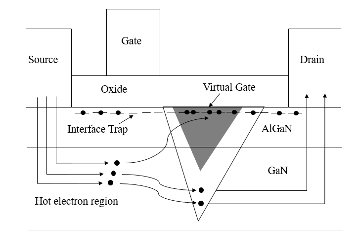
Figure l. A scheme of the current collapse mechanism [9].
2.1.2. Electrochemical GaN oxidation. When the GaN surface is subjected to specific conditions such as high temperature, moisture, and device current, oxygen can react with it, which results in erosion at the place near gate edges. As a consequence, the parasitic resistance increases, and transconductance decreases, leading to a reduction in the device’s performance [10].
The gate will be structurally damaged as a result of the electrochemical dissolution of GaN after long operation. Electrochemical dissolution is associated with water vapor. F. Gao et al [11] showed that water from the environment and the surface of the passivation layer is an important reason for the formation of surface pits. Oxygen is another factor associated with electrochemical dissolution. P. G. Whiting et al [12] made EDS/EELS analyses via STEM and GRTEM. The results showed that the interfacial defect is caused by the formation of an amorphous AlO layer.
2.1.3. Inverse piezoelectric effect. When subjected to high voltage, AlGaN/GaN experiences stress and strain due to its piezoelectric nature, which can result in the formation of lattice defects or even cracks. These cracks and defects can result in parasitic resistance and increased gate leakage current [13]. The degradation degree is related to temperature. Low temperatures can alleviate the inverse piezoelectric effect and reduce unalterable degradation, but more severe reductions in drain current and maximum transconductance are likely to occur [14]. J.A. del Alamo et al [15] discovered that high electric fields create mechanical stress in the AlGaN layer, resulting in increased elastic energy. This can lead to the formation of electrically active lattice defects, which can cause gate leakage current and electron trapping effects. According to this mechanism, the characteristics of the AlGaN layer, such as thickness and composition, are factors that affect device reliability as they change the initial elastic energy level in the AlGaN. Also, optimizing device structures can prevent high electric fields, thus enhancing GaN HEMT’s reliability. Figure 2 shows the stress situation of GaN HEMT under high VDG. The vertical arrow represents a high field generated under the gate. Horizontal arrows represent the mechanical stress formed in the same region.
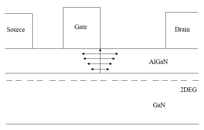
Figure 2. A graphical illustration of GaN HEMT under high VDG [15].
2.2. Thermal reliability issues
Although AlGaN/GaN HEMTs have exceptional performance in high-power, high-frequency phenomena for their unique characteristics, careful thermal management is needed to ensure the device’s efficiency and stability. For instance, a hot spot may form on the gate region in the heating process, which can significantly affect the heat distribution of the device and cause structural damage to devices [16]. Thus, the thermal design of GaN HEMTs needs to be seriously taken into account. This chapter first introduces the simulation of the thermal properties, then some improving methods are discussed.
2.2.1. Numerical simulation. Considering that GaN-based HEMTs have substantial applications in high-power systems and power devices, the devices need to handle large power densities. The power dissipated in GaN devices under such circumstances can lead to significant self-heating effects, drastically affecting the devices' electrical characteristics. Therefore, a precise simulation of the thermal distribution in GaN HEMTs and modification of the device structure through simulations are important [17].
In 2001, L.F. Eastman et al [18] applied nonlinear 3D heat spreading simulations to investigate how the maximum channel temperature varies based on the layout geometry and the amount of normalized heat power dissipated. In 2009, F. Bertoluzza et al [19] made a simulation on GaN HEMTs with different geometry, substrate material, passivation, and cooling strategy. It is reported that three-dimensional effects may have a significant effect on the prediction’s reliability. In 2010, Douglas et al [20] noticed a significant difference in the predicted highest temperature between 2D and 3D simulations, which validates the importance of conducting 3D analyses to enhance the precision and dependability of simulation.
In the case of multi-finger devices, the thermal coupling relies significantly on the device's structure. Symmetric structures can affect cooling conditions, rendering them unsuitable for thermal analysis in practical situations. Thus, it is crucial to comprehend how different structures of multi-finger devices affect thermal distribution. To achieve this goal, Z. Liao et al [16] created a precise 2D finite-element model based on scanning electron microscopy data that matches the dimensions of the actual device. The research takes into account and carefully evaluates the device's structural factors such as gate length, GaN layer thickness, and substrate thickness.
2.2.2. Improving methods. Thermal properties are strongly related to the substrate materials that HEMT devices use. Since diamond is a material with high thermal conductivity, it can be a suitable substrate used to reduce the self-heating effect. T. Liu et al [21] tried integrating diamond substrates with GaN HEMTs to improve heat dissipation and thermal reliability. The direct current characteristics demonstrate a decrease in the self-heating effect, as the device's maximum current density rises, while the peak junction temperature decreases.
The thermal conductivity of AlGaN barrier layers is another factor that affects thermal reliability. Wang et al [22] introduced another layer to the buffer layer, called the back-barrier layer. Its thickness created a thermal barrier layer that impacted the device's reduction in thermally induced current during high-power operation. This method not only enhanced the thermal performance but also increased the device's withstand voltage, which resulted in a decrease in the current collapse effect.
3. Challenges for GaN HEMTs
In recent years, GaN HEMT technology is quickly developing, during which many challenges have shown up, waiting for designers to solve. Herein, challenges are divided into electrical-related and thermal-related problems.
2.3. Electrical-related challenges
GaN HEMT electrical reliability problems are related to many aspects, such as working conditions and structural materials. Under different situations, GaN HEMT has varied electrical stability, making it hard to reach theoretically predicted high performance in real-world applications. Some specific challenges in electrical reliability are listed below.
Trapping effects during the operation of AlGaN/GaN HEMTs are significant obstacles that cause performance degradation, such as reduction in transconductance, output power, and drain and gate lag [23].
In terms of material problems, GaN devices are likely to suffer from electrochemical oxidation in long-term use. Metal can react with water and oxygen, which leads to interfacial defects. The piezoelectric nature of GaN can result in parasitic resistance and increased gate leakage current, negatively affecting its electrical reliability. For future development, researchers need to reduce the negative effects that internal defect of materials brings about.
2.4. Thermal-related challenges
As for thermal reliability issues, careful device thermal management is crucial for producing reliable and robust GaN HEMTs. Ahead of improving the thermal design, precise numerical simulations of the device’s thermal characteristics are required to study the underlying thermal transport mechanisms. However, simulating the thermal distribution of GaN HEMTs with high accuracy is a challenging task. This is because accurately modeling the structures requires considering the various nature of materials and trapping effects on bulk and surface [19]. Apart from challenges in simulation, the structure material also faces challenges. The material of extrinsic substrates is essential for devices’ thermal characteristics. Normally, materials with higher thermal conductivity are preferred. However, some high thermal conductivity materials may be incompatible with other substrate materials. For example, diamond, known as a high thermal conductivity material, is not a satisfying option because of the GaN-diamond lattice mismatch [24]. Further investigation is needed to solve those challenges.
4. Conclusion
This paper reviewed the reliability issues of GaN HEMTs. The factors that cause the decrease in devices’ performance include the electric field, temperature, and material characteristics. Electric field distribution can be controlled effectively by surface passivation, gate structure modification, and a barrier layer. By optimizing the process of the device, its robustness against the oxidation mechanism can be significantly improved. By improving the device’s thermal characteristics, crystal damage related to thermal mechanical stress can be prevented.
The performance that GaN HEMT shows up in the real world is much lower than its theoretical performance. Once the reliability problems of GaN HEMT are solved, its performance has the potential to rise largely. But for the foreseeable future, GaN HEMT reliability issues will remain a limiting factor that needs further study to overcome.
References
[1]. Yao Z W, Zhu H, Li Y L and Xie N 2023 Investigation of trap characteristics under the inverse piezoelectric effect in AlGaN/GaN HEMT devices at room temperature and low temperature Semiconductor Science and Technology 38 5.
[2]. F. Donmezer 2013 Multiscale electro-thermal modeling of AlGaN/GaN heterostructure field effect transistors Engineering.
[3]. Khan M A, Shur M S, Chen Q C and Kuznia J N 1994 Current/voltage characteristic collapse in AlGaN/GaN heterostructure insulated gate field effect transistors at high drain bias Electronics Letters 30 2175.
[4]. Klein P B, Freitas Jr J A, Binari S C and Wickenden A E 1999 The impact of surface states on the DC and RF characteristics of AlGaN/GaN HFETs IEEE Transactions on Electron Devices 75 4016.
[5]. Vetury R, Zhang N Q, Keller S and Mishra U K 2001 Observation of deep traps responsible for current collapse in GaN metal–semiconductor field-effect transistors Applied Physics Letters 48 560.
[6]. Mizutani T, Ohno Y, Akita M, Kishimoto S and Maezawa K 2003 A Study on Current Collapse in AlGaN/GaN HEMTs Induced by Bias Stress Applied Physics Letters 50 2015.
[7]. Faqir M, Bouya M, Malbert N, Labat N, Carisetti D, Lambert B, Verzellesi G and Fantini F 2010 Analysis of current collapse effect in AlGaN/GaN HEMT: Experiments and numerical simulations Microelectronics Reliability 50 1520.
[8]. Saptarsi Ghosh, Subhashis Das, Syed Mukulika Dinara, Ankush Bag and Apurba Chakraborty 2018 OFF-State Leakage and Current Collapse in AlGaN/GaN HEMTs: A Virtual Gate Induced by Dislocations IEEE Transactions on Electron Devices 65 1333.
[9]. Pichingla Kharei, Achinta Baidya, Niladri Pratap Maity and Reshmi Maity 2023 An insight to current collapse in GaN HEMT and suppressing techniques Engineering Research Express 5.
[10]. Enrico Zanoni, Fabiana Rampazzo, Carlo De Santi, Gao Z, Chandan Sharma, Nicola Modolo, Giovanni Verzellesi, Alessandro Chini, Gaudenzio Meneghesso and Matteo Meneghini 2022 Failure Physics and Reliability of GaN-Based HEMTs for Microwave and Millimeter-Wave Applications: A Review of Consolidated Data and Recent Results Applications and Material Science 219.
[11]. Gao F, Swee Ching Tan, Jesús A. del Alamo, Carl V. Thompson and Tomás Palacios 2013 Impact of Water-Assisted Electrochemical Reactions on the OFF-State Degradation of AlGaN/GaN HEMTs IEEE Transactions on Electron Devices 61 437.
[12]. Whiting P G, Holzworth M R, Lind A G, Pearton S J, Jones K S, Liu L, Kang T S, Ren F and Xin Y 2017 Erosion defect formation in Ni-gate AlGaN/GaN high electron mobility transistors Microelectronics Reliability 70 32.
[13]. Kaushik Mazumdar, Sanam Kala and Aniruddha Ghosal 2019 Nanocrack formation due to inverse piezoelectric effect in AlGaN/GaN HEMT Superlattices and Microstructures 125 120.
[14]. Zhu Q, Ma X H, Hou B, Wu M, Zhu J J, Yang L and Zhang M 2020 Investigation of Inverse Piezoelectric Effect and Trap Effect in AlGaN/GaN HEMTs Under Reverse-Bias Step Stress at Cryogenic Temperature IEEE Access 8 35520.
[15]. Alamo J A del and Joh J 2009 GaN HEMT reliability Microelectronics Reliability s 49 1200.
[16]. Liao Z H, Guo C S, Meng J, Jiang B Y, Gao L, Su Y, Wang R M and Feng S W 2017 Thermal evaluation of GaN-based HEMTs with various layer sizes and structural parameters using finite-element thermal simulation Microelectronics Reliability 74 52.
[17]. Turin Valentin O and Balandin Alexander A 2006 Electrothermal simulation of the self-heating effects in GaN-based field-effect transistors Journal of Applied Physics 100.
[18]. Eastman L F, Tilak V, Smart J, Green B M, Chumbes E M, Dimitrov R, Kim Hyungtak and Ambacher O S 2001 Undoped AlGaN/GaN HEMTs for microwave power amplification IEEE Transactions on Electron Devices 48 479.
[19]. Bertoluzza F, Delmonte N and Menozzi R 2009 Three-dimensional finite-element thermal simulation of GaN-based HEMTs Microelectronics Reliability 49 468.
[20]. Douglas E A, Ren F and Pearton S J 2011 Finite-element simulations of the effect of device design on channel temperature for AlGaN/GaN high electron mobility transistors Journal of Vacuum Science & Technology B 29.
[21]. Liu T T, Kong Y C, Wu L S, Guo H X, Zhou J J, Kong C and Chen T S 2017 3-inch GaN-on Diamond HEMTs With Device-First Transfer Technology IEEE Electron Device Letters 38 1417.
[22]. Wang H Y, Chiu H C, Hsu W C, Liu C M, Chuang C Y, Liu J Z and Huang Y L 2020 The Impact of AlxGa1−xN Back Barrier in AlGaN/GaN High Electron Mobility Transistors (HEMTs) on Six-Inch MCZ Si Substrate Coatings 10.
[23]. Binari S C, Ikossi K, Roussos J A, Kruppa W, Park Doewon, Dietrich H B and Koleske D D 2001 Trapping effects and microwave power performance in AlGaN/GaN HEMTs IEEE Transactions on Electron Devices 48 465.
[24]. Muhaimin Haziq, Shaili Falina, Asrulnizam Abd Manaf, Hiroshi Kawarada and Mohd Syamsul 2022 Challenges and Opportunities for High-Power and High-Frequency AlGaN/GaN High-Electron-Mobility Transistor (HEMT) Applications: A Review Micromachines 13.
Cite this article
Shu,T. (2023). Reliability issues of GaN HEMT: Current status and challenges. Applied and Computational Engineering,23,238-244.
Data availability
The datasets used and/or analyzed during the current study will be available from the authors upon reasonable request.
Disclaimer/Publisher's Note
The statements, opinions and data contained in all publications are solely those of the individual author(s) and contributor(s) and not of EWA Publishing and/or the editor(s). EWA Publishing and/or the editor(s) disclaim responsibility for any injury to people or property resulting from any ideas, methods, instructions or products referred to in the content.
About volume
Volume title: Proceedings of the 2023 International Conference on Functional Materials and Civil Engineering
© 2024 by the author(s). Licensee EWA Publishing, Oxford, UK. This article is an open access article distributed under the terms and
conditions of the Creative Commons Attribution (CC BY) license. Authors who
publish this series agree to the following terms:
1. Authors retain copyright and grant the series right of first publication with the work simultaneously licensed under a Creative Commons
Attribution License that allows others to share the work with an acknowledgment of the work's authorship and initial publication in this
series.
2. Authors are able to enter into separate, additional contractual arrangements for the non-exclusive distribution of the series's published
version of the work (e.g., post it to an institutional repository or publish it in a book), with an acknowledgment of its initial
publication in this series.
3. Authors are permitted and encouraged to post their work online (e.g., in institutional repositories or on their website) prior to and
during the submission process, as it can lead to productive exchanges, as well as earlier and greater citation of published work (See
Open access policy for details).
References
[1]. Yao Z W, Zhu H, Li Y L and Xie N 2023 Investigation of trap characteristics under the inverse piezoelectric effect in AlGaN/GaN HEMT devices at room temperature and low temperature Semiconductor Science and Technology 38 5.
[2]. F. Donmezer 2013 Multiscale electro-thermal modeling of AlGaN/GaN heterostructure field effect transistors Engineering.
[3]. Khan M A, Shur M S, Chen Q C and Kuznia J N 1994 Current/voltage characteristic collapse in AlGaN/GaN heterostructure insulated gate field effect transistors at high drain bias Electronics Letters 30 2175.
[4]. Klein P B, Freitas Jr J A, Binari S C and Wickenden A E 1999 The impact of surface states on the DC and RF characteristics of AlGaN/GaN HFETs IEEE Transactions on Electron Devices 75 4016.
[5]. Vetury R, Zhang N Q, Keller S and Mishra U K 2001 Observation of deep traps responsible for current collapse in GaN metal–semiconductor field-effect transistors Applied Physics Letters 48 560.
[6]. Mizutani T, Ohno Y, Akita M, Kishimoto S and Maezawa K 2003 A Study on Current Collapse in AlGaN/GaN HEMTs Induced by Bias Stress Applied Physics Letters 50 2015.
[7]. Faqir M, Bouya M, Malbert N, Labat N, Carisetti D, Lambert B, Verzellesi G and Fantini F 2010 Analysis of current collapse effect in AlGaN/GaN HEMT: Experiments and numerical simulations Microelectronics Reliability 50 1520.
[8]. Saptarsi Ghosh, Subhashis Das, Syed Mukulika Dinara, Ankush Bag and Apurba Chakraborty 2018 OFF-State Leakage and Current Collapse in AlGaN/GaN HEMTs: A Virtual Gate Induced by Dislocations IEEE Transactions on Electron Devices 65 1333.
[9]. Pichingla Kharei, Achinta Baidya, Niladri Pratap Maity and Reshmi Maity 2023 An insight to current collapse in GaN HEMT and suppressing techniques Engineering Research Express 5.
[10]. Enrico Zanoni, Fabiana Rampazzo, Carlo De Santi, Gao Z, Chandan Sharma, Nicola Modolo, Giovanni Verzellesi, Alessandro Chini, Gaudenzio Meneghesso and Matteo Meneghini 2022 Failure Physics and Reliability of GaN-Based HEMTs for Microwave and Millimeter-Wave Applications: A Review of Consolidated Data and Recent Results Applications and Material Science 219.
[11]. Gao F, Swee Ching Tan, Jesús A. del Alamo, Carl V. Thompson and Tomás Palacios 2013 Impact of Water-Assisted Electrochemical Reactions on the OFF-State Degradation of AlGaN/GaN HEMTs IEEE Transactions on Electron Devices 61 437.
[12]. Whiting P G, Holzworth M R, Lind A G, Pearton S J, Jones K S, Liu L, Kang T S, Ren F and Xin Y 2017 Erosion defect formation in Ni-gate AlGaN/GaN high electron mobility transistors Microelectronics Reliability 70 32.
[13]. Kaushik Mazumdar, Sanam Kala and Aniruddha Ghosal 2019 Nanocrack formation due to inverse piezoelectric effect in AlGaN/GaN HEMT Superlattices and Microstructures 125 120.
[14]. Zhu Q, Ma X H, Hou B, Wu M, Zhu J J, Yang L and Zhang M 2020 Investigation of Inverse Piezoelectric Effect and Trap Effect in AlGaN/GaN HEMTs Under Reverse-Bias Step Stress at Cryogenic Temperature IEEE Access 8 35520.
[15]. Alamo J A del and Joh J 2009 GaN HEMT reliability Microelectronics Reliability s 49 1200.
[16]. Liao Z H, Guo C S, Meng J, Jiang B Y, Gao L, Su Y, Wang R M and Feng S W 2017 Thermal evaluation of GaN-based HEMTs with various layer sizes and structural parameters using finite-element thermal simulation Microelectronics Reliability 74 52.
[17]. Turin Valentin O and Balandin Alexander A 2006 Electrothermal simulation of the self-heating effects in GaN-based field-effect transistors Journal of Applied Physics 100.
[18]. Eastman L F, Tilak V, Smart J, Green B M, Chumbes E M, Dimitrov R, Kim Hyungtak and Ambacher O S 2001 Undoped AlGaN/GaN HEMTs for microwave power amplification IEEE Transactions on Electron Devices 48 479.
[19]. Bertoluzza F, Delmonte N and Menozzi R 2009 Three-dimensional finite-element thermal simulation of GaN-based HEMTs Microelectronics Reliability 49 468.
[20]. Douglas E A, Ren F and Pearton S J 2011 Finite-element simulations of the effect of device design on channel temperature for AlGaN/GaN high electron mobility transistors Journal of Vacuum Science & Technology B 29.
[21]. Liu T T, Kong Y C, Wu L S, Guo H X, Zhou J J, Kong C and Chen T S 2017 3-inch GaN-on Diamond HEMTs With Device-First Transfer Technology IEEE Electron Device Letters 38 1417.
[22]. Wang H Y, Chiu H C, Hsu W C, Liu C M, Chuang C Y, Liu J Z and Huang Y L 2020 The Impact of AlxGa1−xN Back Barrier in AlGaN/GaN High Electron Mobility Transistors (HEMTs) on Six-Inch MCZ Si Substrate Coatings 10.
[23]. Binari S C, Ikossi K, Roussos J A, Kruppa W, Park Doewon, Dietrich H B and Koleske D D 2001 Trapping effects and microwave power performance in AlGaN/GaN HEMTs IEEE Transactions on Electron Devices 48 465.
[24]. Muhaimin Haziq, Shaili Falina, Asrulnizam Abd Manaf, Hiroshi Kawarada and Mohd Syamsul 2022 Challenges and Opportunities for High-Power and High-Frequency AlGaN/GaN High-Electron-Mobility Transistor (HEMT) Applications: A Review Micromachines 13.