


1. Introduction
Integrated circuits play a crucial role in various electronic applications, ranging from computers and smartphones to automotive systems and medical devices. The invention of the integrated circuit revolutionized the electronics industry by enabling the integration of complex electronic functions onto a small chip, leading to the development of smaller, faster, and more powerful electronic devices [1]. With the continual development of manufacturing technology, planar MOSFETs are increasingly miniaturized, resulting in a reduction in channel length. The scaling of planer MOSFET was predicted to be limited to 15nm due to fundamental physical limitations, but it has already ended at 32nm technology node due to difficulties in maintaining gate coupling of devices with planer structure. During the past fifty years, blessed by Moore's Law, predicting that "the performance of computer purchased at the same price doubles every 18 months", the IC industry has been developing at a considerable speed. However, according to IRDS (International Roadmap for Devices and Systems™), Moore's Law will no longer be in force. Therefore, two paths have been proposed to develop the IC industry further – "More Moore" and "More than Moore".
In terms of "More Moore", developments are explored following the trace of traditional scaling. When the feature size of devices was scaled down to about 10nm and below, concerning the traditional planar process, the gate length became too short to restrain the leakage current. So then, 3D geometry comes to the stage.
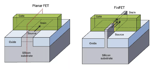
Figure 1. Structure of Planar FET versus FinFET.
The FinFET (Fin Field-Effect Transistor), as is shown in figure 1., is proposed to overcome certain limitations of planar transistor designs, which have a vertical fin-like structure protruding from the semiconductor substrate. The fin structure serves as the conducting channel between the source and drain terminals of the transistor. Therefore, the larger surface area created between the gate and channel provides better control of the electric state and reduces leakage compared to planar FETs. In the past decades, FinFET has been progressing prosperously. Many supporting technologies have been developed, which enabled Moore's Law to carry on to about 5nm nodes. However, when scaling down further to about 3nm nodes, the potential of FinFET is limited. There are many challenges. For example, the width of the fin should be decreased to curb short channel effects and physical limit and larger parasitic capacitance faced during scaling down [2]. Short channel effect refers to a phenomenon that occurs when the length of the channel is equal to the width of the depletion layer in the source and drain junctions [1]. One significant short-channel effect is drain-induced barrier lowering (DIBL). In traditional transistors, the channel region separates the source and drain terminals, controlling the current flow between them. As the channel length decreases, the electric field from the drain terminal starts to penetrate into the channel region, causing a reduction in the effective barrier height at the source end. This lowering of the barrier height reduces the control the gate voltage has over the channel, resulting in increased leakage current and reduced transistor performance.
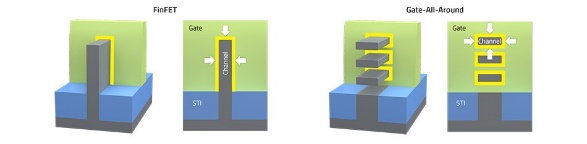
Figure 2. Structure of FinFET versus Gate-all-around FET(GAAFET).
To mitigate the short-channel effects, various techniques have been developed. Multi-gate devices, such as triple-gate and Gate-All-Around Field-Effect Transistor (GAAFETs), have been proposed to reduce SCEs in order to continue Moore's Law and maintain device performance. Gate-All-Around Field-Effect Transistor (GAAFET) made of vertically stacked horizontal nanosheets is considered the most promising candidate for FinFET replacement [3]. The gate-all-around structure helps reduce DIBL, and maintains a steep subthreshold slope, resulting in improved transistor performance and reduced power dissipation. Moreover, strained Silicon, Silicon on Insulator (SOI), high κ insulator (HK), metal gate, and non-uniform doping are applied to reduce SCEs and enhance device performance. Figure 2 shows the structure of GAAFET. In GAAFET, the channel in FinFET is rotated 90° and stacked horizontally. In this way, the channel can be surrounded by the gate on all sides, as a result, the contact area between the gate and the channel is further increased. Moreover, due to its reduced characteristic length, GAAFET has good gate control, which causes the lowest subthreshold leakage current [4]. Its unique architecture allows the gate to surround the channel region from all sides, providing superior electrostatic control. This results in enhanced gate control over the channel and reduced leakage currents [5]. To mitigate gate leakage current, researchers came up with the solution of using various stack high-κ materials in the gate stack in addition to gate oxide.
Research shows that thanks to the benefits of large effective width, GAAFET with stacked nanosheet, which refers to the shape of the channel in this type of GAAFET, offers versatile design options for performance and power management. It also has superior electrostatics and dynamic performance compared to extremely scaled FinFETs with multiple threshold and isolation solutions inherited from FinFET technologies. All these advantages make stacked Nanosheet devices an attractive solution as a replacement for FinFETs, scalable to the 5nm device node and beyond, and with less complexity in the patterning strategy [1].
So according to the prediction shown in figure 3, the transition from FinFET to GAAFET has been reached.
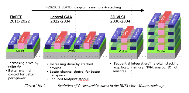
Figure 3. Evolution of device architectures in the IRDS More Moore roadmap [6].
In the following sections, we will introduce the history and current development of GAAFET.
2. Historical developments
The history of Gated-All-Around Field-Effect Transistors (GAAFET) began with the development of Metal-Oxide-Semiconductor Field-Effect Transistors (MOSFET). MOSFET is a type of field-effect transistor with an insulated gate that determines the conductivity of the device based on its voltage. The MOSFET controls the conductivity between the drain terminals and its source based on the amount of voltage applied to their terminal. MOSFET is one of the most produced products on planet Earth with more than 13 sextillion units manufactured as of 2018. The MOSFET is one of the most widely used transistors today with 99.9% of transistors being MOSFETs. However, as integrated circuits became smaller and more delicate, the demands of nanoscale transistors increased. Most MOSFETs started to face challenges due to power leakage currents scalability and power consumption. To solve this issue, engineers created an alternative design where the transistor is three-dimensional instead of planar. The idea was introduced by Hitachi Central Research Laboratory's Digh Hisamoto, Toru Kaga, Youshifumi Kawamoto and Eii Takeda in 1989 and named the Depleted Lean-channel Transistor (DELTA). This innovation allowed a refined control of the transistor during operation The group's work was recognized by the Defense Advanced Research Projects Agency of the United States (DARPA), and granted a contract to conduct research at the University of California at Berkeley with the research group led by Hisamoto along with Chenming Hu from Taiwan Semiconductor Company The group developed many different types of FinFETs between 1998 and 2004, making many breakthroughs in transistor technology. FinFETs successfully improved the control of current flow and employed multiple gates on its fin structures, which enhanced the electrostatic control and reduced leakage. In addition, FinFET is a significant milestone for transistors by continuing Moore's Law. Despite FinFET being successful, the same problems of leakage currents and short channel effects occurred when scaling the transistors down to 5nm and 3nm. Thus, a new technology to address such an issue Gated-All-Around transistor (GAAFET) is created. GAAFET was first introduced in 1988 by Toshiba ULSI Research Center. Unlike FinFET, which encloses its channel on three sides by the gate, GAAFET encloses the entire channel with the gate, hence the name "gated-all-around." GAAFETs are better than FinFETs in a lot of different areas. For example, it is better at controlling short-channel effects, and electrostatic, has better scalability, and enhances energy more efficiently. As the development of GAAFET continues, its functionality is further improved by the use of nanosheets instead of nanowires in the multibridge-channel field-effect transistor (MBCFET). Samsung redesigned and applied the GAA structure to the multi-bridge channel patent. When comparing MBCFETs to FinFETs, it costumes 50% less power, improves 30% better performance and reduces 45% less area. In addition, MBCFETs are compatible with FinFETs designs. Thus, designers could replace FinFETs with MBCFETs without footprints. However, one disadvantage of GAAFETs is that the transistor is much more delicate and the fabrication process is more difficult as a result. All in all, GAAFET is still in development. It is the hope of future transistor technology that will continue Moore's Law. [6-8]
3. Current state of GAAFET
Considering that the structure of GAAFET was proposed to carry on the development path of "More Moore'', in other words, the goal is to tap the potential of current microelectronics technology, which is based on silicon. So, it's necessary first to clarify the limits of silicon technology and then implement optimizations within the limits.
3.1. Limits of silicon-based microelectronics technology
The theoretical foundations of microelectronics include electromagnetics, quantum mechanics, thermodynamics, and so on. Since in integrated circuits, information is stored, processed, and transmitted by controlling the motion of the charge carriers in a medium such as doped silicon, and the motion of the charge carriers inevitably follows a series of fundamental physical laws, which are independent of specific structure, process technology and other factors, the development in microelectronics technology cannot surpass these basic physical laws. Therefore, basic physical laws impose the first constraint.
Looking further, microelectronics technology today is mainly built on silicon-based materials. So features of the material, or silicon, will further narrow down the constraints based on the laws of physics mentioned above [9,10].
In addition to these fundamental theoretical limits, the performance of devices is also subject to many practical limits, including limits at the circuit and system level, limits in fabrication and process, and limits inherent in semiconductor devices.
3.1.1. Fundamental limits. In terms of electromagnetics, based on the Uncertainty Principle, the change of the energy E which can be observed during the switch delay time \( {t_{d}} \) is limited by. \( E{∙t_{d}}≫h \) . In this case, the minimum power of the device is \( \frac{h}{t_{d}^{2}} \) . In terms of thermal dynamics, to change the state of the electron gas in the channel, the minimum energy needed is \( kTln{2} \) . In this case, the minimum power of the device is \( \frac{1}{{t_{d}}}∙kTln{2} \) . These two results combine to delineate the red area in figure 4, which shows the forbidden area given by basic physical laws.
The properties of materials, such as permittivity \( ϵ \) , breakdown electric field strength \( {E_{c}} \) , and electron saturation velocity \( {v_{s}} \) , etc., then place limits in three facets - switching energy ( \( P \gt ϵ∙\frac{1}{2}\frac{V_{0}^{2}}{{E_{c}}}∙\frac{1}{{t_{d}}} \) ), transit time ( \( {t_{d}} \gt \frac{{V_{0}}}{{v_{s}}∙{E_{c}}} \) ), and thermal conductance ( \( P \lt (πK{v_{s}}ΔT)∙{t_{d}} \) ) [9,10]. They line out the orange part in figure 4, which shows the forbidden area given by materials.
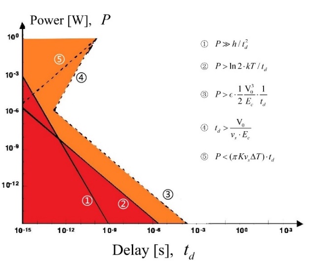
Figure 4. Power versus delay time. The red and orange zones are forbidden by fundamental and material limits.
3.1.2. Practical limits
3.1.2.1 Circuit and system. The persistent drive for higher performance and lower power in electronic systems is pushing semiconductor transistor systems to their limits. In this section, we will look at these restrictions from a variety of angles, including static transfer curves, switching energy, latency, signal contamination, performance volatility, architectural limits, heat dissipation, and reliability concerns. These difficulties' complexities highlight the need for a more integrated, inventive, and multidisciplinary approach to semiconductor system design and manufacture. Because of the world's reliance on electronic systems, ongoing breakthroughs in semiconductor technologies are required. However, as these technologies expand, inherent limitations and challenges emerge, affecting system performance, energy efficiency, and dependability.
Circuit and system limits coexist in a complicated web of complexity and precision in the realm of semiconductor transistor systems. The static transfer curve limit, where the signal voltage swing of a CMOS digital logic circuit must comply with a predetermined limitation ( \( {V_{dd}}≥2(ln{2})kT∕q≥0.038V \) ) to enable reliable binary signal transitions, is a significant aspect at the circuit level. This need originates from the basic functionality of the most common static CMOS logic circuit family, in which the binary signal swing is designed to equal the supply voltage under ideal conditions. For this situation, we'll choose T = 300°C as the average temperature and q as the charge of a single electron.
Another important circuit restriction is switching energy, which specifies the energy transferred during the binary transition of an inverter, the most fundamental unit in the CMOS logic family. This energy is expressed as \( E=(1∕2){C_{c}}{({V_{dd}})^{2}} \) , where \( {C_{c}} \) denotes the capacitance loading the circuit's output terminals. This mathematical relationship shows how the energy involved in switching is directly proportional to the voltage supply and the output capacitance of the circuit, influencing the overall energy consumption of the circuit.
Limits on latency and signal contamination add to the difficulties at the circuit level. When the total resistance of the connection is minimal in comparison to its characteristic impedance, \( {Z_{o}} \) , and the output resistance of the driver equals \( {Z_{o}} \) , delay is minimized. However, signal integrity might be compromised due to undesired noise created by mutual inductance and capacitance between circuit components. This noise, known as "crosstalk," can have a significant impact on the performance and reliability of the circuit, necessitating careful design and layout tactics to limit these impacts.
Many factors contribute to performance fluctuations in semiconductor transistor systems, including internal and extrinsic manufacturing variances, temperature variations, and supply voltage changes. These variations frequently cause increased propagation delay and power consumption, preventing circuit performance from reaching nominal physical limitations. It is critical to address these factors during the design and production phases to guarantee that the circuits operate optimally.
As one moves beyond the circuit level, system-level issues such as architectural restrictions, switching energy limits, and heat dissipation become important. Channel length scaling, gate stack scaling, fabrication complexity, and strain engineering are all challenges for semiconductor technology advancement. These challenges, together with the issues of diversity in transistor properties and manufacturing technologies, necessitate novel solutions in order to continue Moore's law's constant advancement.
The equation \( E=(1∕2){C_{c}}{({V_{dd}})^{2}} \) defines switching energy at the system level, underlining the significance of energy-efficient designs in current electronic systems. Because \( {V_{dd}} \) is calculated by minimizing the sum of switching and static energy dissipation throughout a clock cycle, careful calibration of this value is required to achieve a balance between performance and power consumption.
Heat dissipation has become a key concern in current chip design as a result of increased transistor integration and the complexity of integrated circuits. The difficulty is that while power supply voltage lowers with the device's downsizing, overall power density increases due to a greater number of transistors integrated into the chip. Heat removal is generally limited by packing technology, which has an impact on chip performance and maximum clock frequency, emphasizing the significance of sophisticated cooling methods in electronic system design.
Finally, as device feature sizes shrink, the difficulty of dependability becomes more apparent, particularly when the gate oxide layer thins. The shrinking and increasing density of transistors cause a slew of reliability difficulties, including gate oxide breakdown, hot carrier injection, and electrostatic discharge.
3.1.2.2 Fabrication and process. In traditional planar FET processing, steps include growing crystal, cleaning, photolithographing, etching, oxidating, diffusing, ion implanting, film depositing, and back-end processes, etc., in which the key technology lies in the processing of fine lines, that is, photolithography.
Photolithography technology development focuses on optimizing two parameters - resolution (R) and depth of focus (DOF), and Rayleigh's formula describes them. λ is the wavelength, NA is the numerical aperture, and k1 and k2 are the parameters related to the optical system.
\( R={k_{1}}\frac{λ}{NA}, DOF={k_{2}}\frac{λ}{NA2}\ \ \ (1) \)
To process devices with smaller feature sizes, the value of the resolution R needs to be continuously reduced. And it can be seen from Equation 1 that the reduction of R is achieved by lowering λ, increasing NA, or reducing k1.
In terms of reducing the wavelength λ, the development of lithography can be divided into three stages. From the 1960s to the mid-1980s, contact aligners, proximity aligners, and projection aligners mainly used mercury lamps as light sources, and their spectral lines are g-line(436nm), h-line(405nm), and i-line(365nm), respectively. From the late 1980s to the 2010s, step-and-scan aligners mainly used excimer laser light sources of KrF(248nm) and ArF(198nm). Nowadays, EUV lithography uses extreme ultraviolet light sources with a wavelength of 13.5nm. [11] Together with various resolution enhancement technology, or RET, which reduces k1 by optimizing the optical system structure, processing devices of 3nm node is now possible.
In addition to lithography, deviations occur during oxidation when turning from planar to three-dimensional processes. This is because shaped silicon structures oxidize differently than simple flat surfaces [12]. Some researches on this show some phenomena [13,14]. First, retardation is a significant effect on sharp corners. Second, the retardation is much more noticeable for low-temperature oxidations than it is for high temperatures. Finally, interior(concave) corners show a more marked effect than exterior(convex) corners, although both are significantly retarded compared to flat surfaces. These results are caused by several physical mechanisms, including the oxidation rate being affected by crystal orientation and stress due to volume expansion. Recognizing these changes contributes to the advance of fabrication and process.
3.1.2.3 Limits of semiconductor devices. Due to low power consumption, convenience in integration and scalability, CMOS technology, including the structures and technologies derived from MOSFET, is predicted to continue to dominate the development of microelectronics technology for a long time. Therefore, the features inherent in semiconductor devices also propose significant limits, including the limitations caused by random dopant fluctuation, strong field effect in silicon, and simulation and modeling of devices.
Random Dopant Fluctuation, or RDF, is an intrinsic phenomenon caused by the thermal diffusion of particles. Regarding short-channel devices, the total number of impurity particles is limited. Therefore, the fluctuation of the impurity atoms then accounts for a large ratio, and the macro statistical methods based on a large number of particles are no longer applicable. Moreover, processing steps such as ion implantation and diffusion also introduce random fluctuation to the distribution of atoms. Such random distribution can cause a mismatch of the threshold voltage. In terms of devices such as sense amplifiers and SRAMs, the mismatch can cause a large error. Research [15] shows the relationship between the fluctuation of \( {V_{th}} \) , or \( {δV_{th}} \) , and the doping concentration \( {N_{A}} \) . It indicates that the fluctuation of \( {V_{th}} \) is proportional to \( \sqrt[]{{N_{A}}} \) . Therefore, when the doping level of impurities is low, the effect of RDF will be reduced. This point provides an important reference for the development of semiconductor devices.
Since the supply voltage does not decrease proportionately to the gate length, the electric field intensity will become extremely large when devices are scaled down to sub-10nm. The main strong field effects in silicon are quantization of the inversion channel and degradation of carrier mobility. Because of the quantization of the inversion channel, electrons in the channel can no longer be approximated as a thin layer at the Si-SiO2 interface, instead, it shows a certain distribution. This distribution reduces the equivalent gate oxide capacitor, namely enlarging the equivalent gate oxide thickness, thus weakening the gate control ability over the channels' carriers. Research [16] shows that when the electric field intensity is about 106V/cm, the quantization effect will make the threshold voltage increase by 0.2V. As for the degradation of carrier mobility, research [17] shows that as the electric field intensity increases, the carrier mobility shifts from being limited by surface acoustic phonon to being limited by surface roughness. In this case, the carrier mobility degrades severely under a strong electric field.
Simulation and modeling of devices are important as well, as what is needed are devices with predictable behaviors. The classical model, or the drift-diffusion model, is based on Poisson's equation and current continuity. This model only works when the feature size of the device is much longer than the mean free path of carriers, and the electric field intensity should also be low and change slowly. In this case, carriers can experience a lot of scattering during transit time. However, when devices are scaled down, the feature size becomes small and the electric field intensity becomes large. Then, the classical model becomes invalid. In this case, carriers only experience several scattering events. In light of this observation, many quasi-classical models are set up, such as those which introduce the concepts of Monte Carlo, fluid mechanics, and energy balance equation, etc. [9].
3.2. Development of GAAFET
3.2.1. Junctionless transistor. Junctionless transistors are an innovative type of field-effect transistor (FET) that have gained significant attention in recent years. The p-type piece of silicon that has been doped with impurities to produce an excess of holes and an n-type piece of silicon, which has been doped to produce an excess of electrons come together to form the most typical type of junction, known as the p-n junction [18]. For junctionless transistors, the need for a p-n junction is eliminated, simplifying the manufacturing process and offering several potential advantages. For example, instead of relying on a junction, the junctionless transistor utilizes the concept of channel modulation to control the flow of current.
Because transistors are getting so small, manufacturing high-quality junctions is getting increasingly challenging. Particularly, it is highly challenging to modify a material's doping concentration over distances less than roughly 10 nm. Therefore, junctionless transistors might assist chip manufacturers in creating ever-smaller devices.
Junctionless transistors are proposed, which according to Moore’s Law, can be realized to reduce the transistor’s size and have good performance. Furthermore, Junctionless devices are uniformly doped throughout the source-channel-drain region. Due to the Junctionless nature of the device, the Junctionless Multigate (JL-MG) MOSFETs exhibit an increase in dimensions scalability and high packing density as well as less thermal management and simple fabrication feasibility. On the other hand, the Junctionless GAAFETs have advantages in terms of excellent control over the channel region and reduced susceptibility to SCEs [18].
In junctionless transistors, the electric field perpendicular to the current flow is considerably lower than in conventional inversion mode or accumulation-mode field-effect transistors. Due to the fact that this electric field reduces the inversion channel mobility in metal-oxide semiconductor transistors, the low field in junctionless transistors may provide an advantage in terms of the current drive for manometer-scale complementary metal-oxide semiconductor applications. Junctionless transistors have advantages that reduce power consumption and improve performance. The absence of a junction allows for better electrostatic control of the channel, resulting in lower leakage currents and enhanced short-channel effects.
3.2.2. Using gate stacking and oxidation technique to improve electrostatic performance and SCEs. Gate stacking is employed to improve the electrostatic behaviour of junctionless Gate All-Around (JL-GAA) MOSFETs. Since the conventional planar MOSFET gate stack technology fails to satisfy the requirement when the size of the semiconductor approaches 100nm, which made it is possible to offer field-effect transistors using several gate stack technologies [18]. The high-κ oxide material is layered with an interfacial silicon dioxide (SiO2) layer during gate stacking. Abhinav Gupta et al. studied the oxide engineering technique as an alternative strategy for enhancing the driving current of JL-GAAFETs [3]. There are three device structures proposed, namely, Double Hetero gate oxide (DHGO), Triple Hetero gate oxide (THGO), and Quadruple Hetero gate oxide (QHGO). By applying oxide engineering techniques, these devices are referred to as Junctionless Gate-All-Around (JL-GAA) MOSFETs with various oxide layers, where the device simulation has been undertaken using the 3-D ATLAS TCAD device simulator from SILVACO.
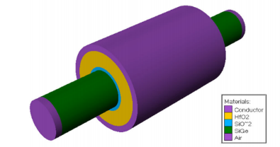
Figure 5. The 3D view of DHGO.
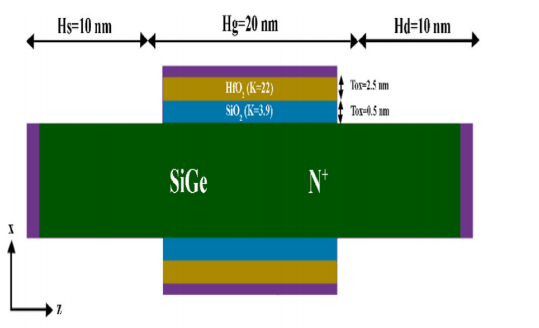
Figure 6. Sectional-view of DHGO.
Among the three structures, it is discovered that DHGO devices have better control of the channel and are more immune to SCEs. Figure 5 depicts the structure of DHGO. The supplementary dimensions of this GAA MOSFET are shown in figure 6, channel thickness, doping concentration. The performance characteristics are Ion=6.85×10⁻⁴ A/μm, Ioff=1.19×10⁻¹¹A/μm, Ion/Ioff=5.8×107, SS=60.67mv/dec, and DIBL= 8.57mV/V.
It is shown that the DHGO JL-GAA MOSFET performs admirably is 81.2% smaller than FinFET's. This structure's subthreshold oscillation is close to the optimal value of 60mv/dec. As an extension of FinFET, DIBL and SS demonstrate that DHGO JLGAA MOSFET has excellent gate control. Furthermore, DHGO JL-GAA MOSFET has good switching characteristics, despite the fact that its Ioff is greater than that of FinFET and its ON/OFF ratio is smaller than that of FinFET. The reason for these occurrences is that the channel of DHGO JL-GAA MOSFET is not as thin as that of FinFET, and is not completely depleted like that of FinFET [18]. In summary, DHGO device architecture is optimal in lower-power and analogue applications. The QHGO devices have better RF performance and are suitable for high-frequency applications [3].
3.2.3. A method proposed by applying asymmetric non-local lateral gaussian doping. JLFETs have a unique structure, good scalability, and high immunity to SCEs. In process steps such as diffusion, ion implantation hinders the realization of homogeneous parametrization in JLFETs. Therefore, various doping modes, such as grated and Gaussian doping are implemented on the channel. In general, Gaussian doping is mainly carried out vertically on the JLFET channel. In Gaussian doping, the doping concentration in the channel region is distributed in a Gaussian or bell-shaped profile. Unlike traditional doping techniques that involve uniformly doping the channel, Gaussian doping allows for a more controlled and gradual transition of doping concentration. Moreover, the electric field across the channel can be more evenly distributed to reduce the impact of short-channel effects.
To reduce the supply voltage and power consumption of electronic devices, the Ferroelectric (FE) materials with negative capacitance (NC) effects are incorporated into the gate stack of conventional FETs to overcome the subthreshold swing (SS). In addition, NCFET is ideally adapted for low-power applications due to its superior control over the channel and high-speed switch to lower the supply voltage and overdrive voltage.
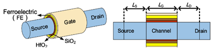
Y. Han et al. proposed an asymmetric LGD NC-JL-GAAFET and investigated by Sentaurus technology computer-aided design (TCAD) numerical simulations [5]. The gate oxide layer is layered with SiO2 and high-κ dielectric HfO2, resulting in a decrease in leakage current and an increase in ION/IOFF. The gate oxide layer is additionally coated with a HfO2-based FE layer with NC effects. The critical manufacturing parameters are specified in Table 1.
(a) (b)
Figure 7. (a) The 3D view of NC-JL-GAAFET (b) Sectional view of NC-JL-GAAFET.
Table 1. Structure parameter for NC-JL-GAAFET in figure 7.
Structure parameter | Value |
Gate Length (LG) | 16 nm |
SiO2 Thickness (TSiO2) | 0.5 nm |
HfO2 Thickness (THfO2) | 1 nm |
Channel Radius (Rchannel) | 3 nm |
Metal Work Function (WK) | 4.5 eV |
Remnant Polarization (Pr) | 5 μC/cm2 |
Coercive Field (Ec) | 1 MV/cm |
In general, the NC effects after stacking FE materials improve the NC-JL-GAAFET performance regarding threshold voltage (VTH), SS, and ION/IOFF. Furthermore, adding Gaussian doping will improve switching performance. There are four different doping modes compared, namely, Uniform doping, Graded doping, local Gaussian doping, and non-local Gaussian doping, as shown in figure 8. The effects of four different doping methods on symmetric and asymmetric structures. The non-local Gaussian doping has superior switching performance and can efficiently reduce DIBL in structure M1 [5].
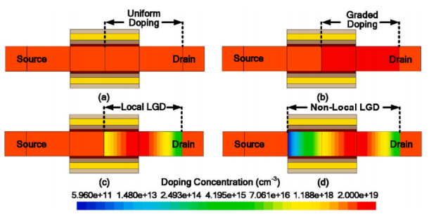
Figure 8. Structures for four doping modes: (a) Uniform (b) Graded (c) Local LGD (d) Non-local LGD.
4. Conclusion
According to the prediction given by IRDS™, the mainstream structure of semiconductor devices will shift to GAA at around 2022 to 2034. GAAFET technology has been developing within the limits of silicon-based technology, including limits at the circuit and system level, limits in fabrication and process, and limits inherent in semiconductor devices, and is now trying to tap potential from various edge-cutting science and technologies. It is gratifying to point out that the development of GAAFET technology has seen notable advancements, such as the junctionless transistor and innovative techniques like gate stacking, oxidation, and asymmetric non-local lateral Gaussian doping. These approaches have shown the potential to improve electrostatic performance, mitigate short-channel effects, and enhance device reliability. The elimination of junctions in the junctionless transistor simplifies fabrication and offers improved control over the channel. Gate stacking and oxidation techniques contribute to better electrostatic control, while asymmetric non-local lateral Gaussian doping enables precise threshold voltage control.
References
[1]. S. Zhang, Review of modern field effect transistor technologies for scaling, in: Journal of Physics: Conference Series, IOP Publishing, vol. 1617, 2020, p. 012054.
[2]. Y. Wu et al., Development and challenges of FinFET and GAA for Sub-3nm CMOS technology node, in: Micro/nano Electronics and Intelligent Manufacturing, vol. 3, no. 1, 2021.
[3]. A. Gupta et al., “A Novel Approach to Investigate the Impact of Hetero-High-K Gate Stack on SiGe Junctionless Gate-All-Around (JL-GAA) MOSFET,” Silicon, Jan. 2021, doi: https://doi.org/10.1007/s12633-020-00860-0.
[4]. S. Priscilla Scarlet, N. Vinodhkumar, R. Srinivasan, "Performance enhancement of junctionless silicon nanotube FETs using the gate and dielectric engineering", Journal of Computational Electronics, vol.20, no.1, pp.209, 2021.
[5]. Y. Han, W. Lü, W. Wei, C. Zhang, and D. Chen, “Optimization of negative capacitance junctionless gate-all-around field-effect transistor using asymmetric non-local lateral Gaussian doping,” Microelectronics Journal, vol. 135, pp. 105760–105760, Mar. 2023, DOI: https://doi.org/10.1016/j.mejo.2023.105760.
[6]. F. Mo, C. E. Spano, Y. Ardesi, M. Ruo Roch, G. Piccinini, and M. Vacca, Ns-gaafet compact modeling: Technological challenges in sub-3-nm circuit performance, in: Electronics, vol. 12, no. 6, p. 1487, 2023.
[7]. M. Badaroglu, More Moore, in: 2021 IEEE International Roadmap for Devices and Systems Outbriefs, IEEE, 2021, pp. 01–38.
[8]. N. A. Kumari and P. Prithvi, Performance evaluation of GAA nanosheet FET with varied geometrical and process parameters, in: Silicon, vol. 14, no. 15, pp. 9821–9831, 2022.
[9]. Y. Wang et al., The Challenges for Physical Limitations in Si Microelectronics, in: Acta Electronica Sinica, vol. 26, no. 11, pp. 77–84, 1998.
[10]. J. D. Meindl, Q. Chen, and J. A. Davis, Limits on silicon nanoelectronics for terascale integration, in: Science, vol. 293, no. 5537, pp. 2044–2049, 2001
[11]. B. Chen, Lithography Technology During the Past Six Decades, in: Laser & Optoelectronics Progress, vol. 59, no. 9, p. 0922031, 2022.
[12]. J. Plummer and M. Deal, Silicon VLSI technology fundamentals, practice and modeling, 2000.
[13]. D.-B. Kao, J. P. McVittie, W. D. Nix and K. C. Saraswat, Two-dimensional thermal oxidation of silicon—I. Experiments, in: IEEE Transactions on Electron Devices, vol. 34, no. 5, pp. 1008-1017, May 1987, DOI: 10.1109/T-ED.1987.23037.
[14]. D.-B. Kao, J. P. McVittie, W. D. Nix and K. C. Saraswat, Two-dimensional thermal oxidation of silicon. II. Modeling stress effects in wet oxides, in: IEEE Transactions on Electron Devices, vol. 35, no. 1, pp. 25-37, Jan. 1988, DOI: 10.1109/16.2412.
[15]. Y. Su and J. Yang, Study on the Influence of Random Doping on the Threshold Voltage of Ultra Deep Submicron SOI MOSFETs, in: Applied Physics, vol. 8, p. 472, 2018.
[16]. A. S. Spinelli, A. Benvenuti and A. Pacelli, Self-consistent 2-D model for quantum effects in n-MOS transistors, in: IEEE Transactions on Electron Devices, vol. 45, no. 6, pp. 1342-1349, June 1998, DOI: 10.1109/16.678567.
[17]. D. Vasileska and D. K. Ferry, Scaled silicon MOSFET's: universal mobility behavior, in: IEEE Transactions on Electron Devices, vol. 44, no. 4, pp. 577-583, April 1997, DOI: 10.1109/16.563361.
[18]. J. Yang, "Gate stack structure applied to field-effect transistor," 2022 International Conference on Applied Physics and Computing (ICAPC), Ottawa, ON, Canada, 2022, pp. 198-204, DOI: 10.1109/ICAPC57304.2022.00044.
Cite this article
Xie,C.;Zhang,Y.;Zhang,K.;Guo,L.Z. (2023). Introduction of Gate-All-Around FET (GAAFET) . Applied and Computational Engineering,28,164-175.
Data availability
The datasets used and/or analyzed during the current study will be available from the authors upon reasonable request.
Disclaimer/Publisher's Note
The statements, opinions and data contained in all publications are solely those of the individual author(s) and contributor(s) and not of EWA Publishing and/or the editor(s). EWA Publishing and/or the editor(s) disclaim responsibility for any injury to people or property resulting from any ideas, methods, instructions or products referred to in the content.
About volume
Volume title: Proceedings of the 2023 International Conference on Mechatronics and Smart Systems
© 2024 by the author(s). Licensee EWA Publishing, Oxford, UK. This article is an open access article distributed under the terms and
conditions of the Creative Commons Attribution (CC BY) license. Authors who
publish this series agree to the following terms:
1. Authors retain copyright and grant the series right of first publication with the work simultaneously licensed under a Creative Commons
Attribution License that allows others to share the work with an acknowledgment of the work's authorship and initial publication in this
series.
2. Authors are able to enter into separate, additional contractual arrangements for the non-exclusive distribution of the series's published
version of the work (e.g., post it to an institutional repository or publish it in a book), with an acknowledgment of its initial
publication in this series.
3. Authors are permitted and encouraged to post their work online (e.g., in institutional repositories or on their website) prior to and
during the submission process, as it can lead to productive exchanges, as well as earlier and greater citation of published work (See
Open access policy for details).
References
[1]. S. Zhang, Review of modern field effect transistor technologies for scaling, in: Journal of Physics: Conference Series, IOP Publishing, vol. 1617, 2020, p. 012054.
[2]. Y. Wu et al., Development and challenges of FinFET and GAA for Sub-3nm CMOS technology node, in: Micro/nano Electronics and Intelligent Manufacturing, vol. 3, no. 1, 2021.
[3]. A. Gupta et al., “A Novel Approach to Investigate the Impact of Hetero-High-K Gate Stack on SiGe Junctionless Gate-All-Around (JL-GAA) MOSFET,” Silicon, Jan. 2021, doi: https://doi.org/10.1007/s12633-020-00860-0.
[4]. S. Priscilla Scarlet, N. Vinodhkumar, R. Srinivasan, "Performance enhancement of junctionless silicon nanotube FETs using the gate and dielectric engineering", Journal of Computational Electronics, vol.20, no.1, pp.209, 2021.
[5]. Y. Han, W. Lü, W. Wei, C. Zhang, and D. Chen, “Optimization of negative capacitance junctionless gate-all-around field-effect transistor using asymmetric non-local lateral Gaussian doping,” Microelectronics Journal, vol. 135, pp. 105760–105760, Mar. 2023, DOI: https://doi.org/10.1016/j.mejo.2023.105760.
[6]. F. Mo, C. E. Spano, Y. Ardesi, M. Ruo Roch, G. Piccinini, and M. Vacca, Ns-gaafet compact modeling: Technological challenges in sub-3-nm circuit performance, in: Electronics, vol. 12, no. 6, p. 1487, 2023.
[7]. M. Badaroglu, More Moore, in: 2021 IEEE International Roadmap for Devices and Systems Outbriefs, IEEE, 2021, pp. 01–38.
[8]. N. A. Kumari and P. Prithvi, Performance evaluation of GAA nanosheet FET with varied geometrical and process parameters, in: Silicon, vol. 14, no. 15, pp. 9821–9831, 2022.
[9]. Y. Wang et al., The Challenges for Physical Limitations in Si Microelectronics, in: Acta Electronica Sinica, vol. 26, no. 11, pp. 77–84, 1998.
[10]. J. D. Meindl, Q. Chen, and J. A. Davis, Limits on silicon nanoelectronics for terascale integration, in: Science, vol. 293, no. 5537, pp. 2044–2049, 2001
[11]. B. Chen, Lithography Technology During the Past Six Decades, in: Laser & Optoelectronics Progress, vol. 59, no. 9, p. 0922031, 2022.
[12]. J. Plummer and M. Deal, Silicon VLSI technology fundamentals, practice and modeling, 2000.
[13]. D.-B. Kao, J. P. McVittie, W. D. Nix and K. C. Saraswat, Two-dimensional thermal oxidation of silicon—I. Experiments, in: IEEE Transactions on Electron Devices, vol. 34, no. 5, pp. 1008-1017, May 1987, DOI: 10.1109/T-ED.1987.23037.
[14]. D.-B. Kao, J. P. McVittie, W. D. Nix and K. C. Saraswat, Two-dimensional thermal oxidation of silicon. II. Modeling stress effects in wet oxides, in: IEEE Transactions on Electron Devices, vol. 35, no. 1, pp. 25-37, Jan. 1988, DOI: 10.1109/16.2412.
[15]. Y. Su and J. Yang, Study on the Influence of Random Doping on the Threshold Voltage of Ultra Deep Submicron SOI MOSFETs, in: Applied Physics, vol. 8, p. 472, 2018.
[16]. A. S. Spinelli, A. Benvenuti and A. Pacelli, Self-consistent 2-D model for quantum effects in n-MOS transistors, in: IEEE Transactions on Electron Devices, vol. 45, no. 6, pp. 1342-1349, June 1998, DOI: 10.1109/16.678567.
[17]. D. Vasileska and D. K. Ferry, Scaled silicon MOSFET's: universal mobility behavior, in: IEEE Transactions on Electron Devices, vol. 44, no. 4, pp. 577-583, April 1997, DOI: 10.1109/16.563361.
[18]. J. Yang, "Gate stack structure applied to field-effect transistor," 2022 International Conference on Applied Physics and Computing (ICAPC), Ottawa, ON, Canada, 2022, pp. 198-204, DOI: 10.1109/ICAPC57304.2022.00044.