


1. Introduction
In the race of the modern Very Large-Scale Integrated Circuit (VLSI) industry, power consumption and circuitry speed both become critical factors in evaluating a chip. John Bardeen, Walter Brattain, and William Shockley built the first point contact germanium transistor on December 23, 1947, praised as "a magnificent Christmas present" for the first semiconductor amplifier. The development of transistors, which ushered in the microelectronics revolution, was a significant invention of the 20th century. The story of transistors, which ushered in the microelectronics revolution, was an important invention of the 20th century. After the appearance of transistors, large and power-consuming electron tubes could be replaced by compact and low-power electrons. The story of transistors provided a solid foundation for the integrated circuits later on. In the 20th century, communication systems began to use semiconductor materials. In the first half of the 20th century, the Crystal radio, popular among radio enthusiasts, employed ore as a semiconductor material for detection. Semiconductors' electrical properties have also been used in telephone networks. Later, in the 1960s, Mohamed Atalla and Dawon Kahng introduced a device called metal-oxide-semiconductor field-effect transistor (MOSFET), which is by far the most significant component in modern integrated circuits.
MOSFET has the main advantage over bipolar junction transistors (BJT) and other types of transistors. MOSFET is voltage-based rather than current-based control, implying that the power applied to the input is less vital. This characteristic allows higher transistor density because of the ability to infer heat. Despite energy consumption, large heat generated would cause transistor threshold voltage drop and possible operation failures. Therefore, MOSFET is the most essential transistor for digital chips until now.
Later, in 1965, Gordon Moore observed that the complexity of integrated circuits would double every one and a half years due to increasing demand for chip performance, while the power consumption per unit area would remain the same because of Dennard scaling's prediction. Moore's law summarizes the rate of advancement of information technology. In the more than 50 years since Moore's law was applied, computers have evolved from enigmatic behemoths to vital tools for most people. From laboratories, information technology has penetrated countless everyday families. The Internet has brought the entire world together. Multimedia audio-visual devices have improved everyone's life. Over the last 50 years, Moore's prediction of semiconductor chip integration has spurred the development of the whole industry and changed the lives of billions of people. MOSFET technology, the main component of digital VLSI chips, must evolve and progress to get higher performance and lower cost per chip. As the planar MOSFET process nodes down-scaling approach the physical limits, shrinking of gate length alone would not be enough when developing next-generation MOSFET.
The planar MOSFET faces its challenge until the process node is down to 22 nm, where gate-oxide leakage and Drain-induced barrier lowering (DIBL) due to the short channel effect impedes the gate-to-channel control. The channel length was about a few micrometers in the early integrated circuit MOSFET process. As the planar MOSFET process continued to develop to 32nm, the gate length could not be reduced proportionally with the device's pitch, and traditional MOSFET structures gradually could not meet the growing of device performance. However, when the gate length approaches 20nm, the ability to control the current sharply decreases, and the leakage rate also increases. Traditional planar MOSFETs have ended, and material changes cannot solve the problem. Therefore, FinFET, also called "Tri-gate transistor" by Intel, a multi-gate MOSFET, was invented to replace planar MOSFET devices. [1]
The source and drain region in the FinFET form a "Fin" like channel above the silicon substrate, allowing up to three surfaces of the gate to touch the source-drain track. With more sides of the gate wrapping around the "Fin," FinFET retains its electrical control over the way, maintaining its importance until the 5 nm era. After reaching the 5 nm node, although extreme ultraviolet (EUV) lithography technology has been used, reducing chip size based on FinFET structure becomes even more difficult. The proximity of the fins, the resurgence of leakage, and the increasing height of the fins make it difficult to maintain an upright structure, and the limitations of physical materials make it more complicated for 3D FinFET transistors to sustain. However, to achieve higher transistor density, the transistor's size gets even smaller, so a new generation of MOSFET needs to be introduced. Consequently, the GAAFET shows up, superseding regular FinFET. [2]
GAAFET is the extension of FinFET. The first GAAFET was exhibited in 1988 by the Toshiba research group. They demonstrated the "surrounding gate transistor" (SGT), a vertical nanowire GAAFET. In 2006, the National Fab Center and the Korea Advanced Institute of Science and Technology (KAIST) developed a 3nm GAAFET transistor, which claimed to be the world's smallest transistor. [3] Current GAAFET technology is being developed and commercialized by large industries, such as Intel, Samsung, and TSMC. They state that the new chip with GAAFET in 3nm scale will present lower power, better performance, and higher transistor density than the standard FinFET chip.
2. GAAFET 3D structure
To introduce the structure of GAAFET, we have first to understand the formation of FinFET. In contrast to planar transistors, FinFET and GAAFET are a type of "non-planar" or "3D" transistor. As shown in Figure 1, the main feature of FinFET is that the channel is composed of tall and thin fins protruding from the silicon substrate. The channel length is the fin length along the source and drain direction. The actual channel width grows dramatically, lowering the ON-resistance of the transistor device. The head and drain region are located at the two ends, and the gate region is touching the top and the two sides of the fin to assist current control. [1] The short channel effect in planar MOSFET devices would be successfully countered by this fin-shaped channel, which strengthens the gate-to-channel control, significantly improves circuit control, and lowers leakage current. As a result, it is now possible to further reduce the transistor's gate length. This property makes it possible to efficiently minimize impurity ions' scattering impact and improve the channel's carrier mobility without needing a heavily doped drain. The source-drain current flow is considerably improved as a result. [3,4]
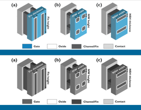
Figure 1. Structural view of (a) FinFET (b)Nanowire GAAFET (c)Nanosheet GAAFET [2]
GAAFET is the variation of FinFET. GAAFET has two structures: Nanowire and Nanosheet, which implies the shape of the transistors' fin, as seen in Figure 1. Unlike classic FinFET, GAAFET is a device where the four sides of the source-drain channel are all surrounded by the gate region. The channel control ability of GAAFET is thus strengthened under the same gate length and width to shrink the transistor size further. Besides, as the contact area between the gate and the channel enlarges, parasitic capacitance and parasitic resistance brought by the new structure should be solved quickly and reduced to a fordable level. [2] It is believed that the production process required by the new system should be similar to that of FinFET, causing existing equipment and technological achievement to be inherited. [4] However, the mass production of GAAFET is still not yet feasible until now, and the yield percentage is undesirable because the manufacturing process of GAAFET is way more complicated than people thought. [5]
The essence of Nanosheet GAAFET is to rotate the fin of regular FinFET by 90 degrees and then stack multiple fins horizontally, all passing through the gate region. As the contact area between the gate and channel of GAAFET becomes larger than common FinFET, the nanosheet's width and the effective channel's width are flexible. In contrast, the fin width in regular FinFET is a fixed value. A more comprehensive sheet can naturally achieve a higher drive current to attain better performance. On the other hand, a narrower sheet occupies a smaller area, which can provide better electrostatic characteristics than regular FinFET and realize shorter gate width and gate length requirements. [5]
The fabrication of Nanosheet GAAFET is distinct. The basic Si/Ge heterostructure is simple to build, and the patterning of the pillar is indistinguishable from FinFETs' fraud. The following processes, nevertheless, are exclusive to nanosheet transistors. An inner spacer will eventually be deposited between the source and drain region, which will subsequently be placed adjacent to the pillar and the space where the gate will ultimately reside due to an indentation in the SiGe layers. This spacer specifies the gate width of the Nanosheet transistor. [5] The SiGe is then removed using a channel release etch once the inner spacers have been inserted. In the small spaces between the silicon nanosheets, atomic layer deposition (ALD) deposits the gate dielectric and metal. The germanium content of the SiGe layers should be reduced as much as feasible to mitigate lattice distortion and other deficiencies. [6-8] The etch selectivity does, however, increase with Ge concentration, and degradation of the silicon layers during inner spacer indentation or channel release etch will affect channel thickness and, consequently, threshold voltage. [8]
Nanowire technology seems to be left behind compared to Nanosheet. In recent years, significant industries have gradually abandoned the manufacture of nanowire GAAFETs and turned to research and fabrication on Nanosheet technologies. This is because the formation of nanowire GAAFET is more complicated than that of nanosheet transistors, and the technical approach differs from previous technology. According to the National Cheng Kung University researchers, when many layers of transistors are integrated on the same silicon substrate, the threshold voltage doping for stacked wires differs significantly from those for traditional approaches. [8] However, it does not satisfy the need for multi-Vt design, frequently utilized in system-on-chip (SoC) applications. [8, 9] Leaving the channel undoped provides a mobility benefit and is anticipated to alleviate the problem of random dopant fluctuation. Instead, several gate work functions will be required for various threshold voltages, making such an undoped method more challenging. [10]
IBM, for example, disclosed a gate all around silicon nanowire FET with a nanowire pitch of 30nm and a gate pitch scaled to 60nm, where its practical nanowire dimension was down to 12.8nm. [8] Two landing pads are created on a silicon substrate during this Nanowire GAAFET manufacturing process. On the landing pads, nanowires are grown and placed horizontally. After that, the protruding nanowires are covered with vertical gates, which stack to establish the gate region. Then, there occurs the formation of the spacer. [8, 11] According to IBM's news report, the silicon nanowires are chopped away from the gate region. In-situ doped silicon epitaxy is then created from the uncovered sectional areas of the silicon nanowires at the spacer's edge. Copper interconnects, and typical self-aligned nickel-based silicide contacts were used to complete the device. [8, 11]
3. Industrial and Commercial prospects
GAAFET's performance is crushing regular FinFET, but it took industries over a decade to transition FinFET to GAAFET. The reason is that GAAFET's manufacturing process complexity increases significantly. Also, device size has shrunk due to the development of more advanced manufacturing techniques and the need for more effective transistors. FinFET also struggles with the short channel effect, mobility degradation, and leakage from quantum tunneling as the effective gate length goes below 6nm. As Figure 2 shows, GAAFET outperforms the pragmatic ultra-thin FinFET due to better suppression of the short channel effect. The on-current and the capacitance generally represent the transistor speed, which could be generalized as the RC delay model. The higher on-current and lower capacitance stands for shorter delay and higher rate. Yet the performance improvement is not significantly related to circuit speed; the control of the quick channel effect is remarkable. As predicted, the subthreshold swing (SS), DIBL, and threshold voltage (Vt) significantly improve the short channel effect, making the GAAFET promising for scaling down to sub 5nm. The temporary channel effect in the device will gradually lower the on-current and enhance the off-current, keeping the leakage power up to produce excessive heating, eventually leading the chip to failure. So, keeping up with today’s high performance and low-power design, GAAFET is the option. Moreover, large industries are battling around the chip's process nodes to keep pace with the competition of digital chipsets PPA, which leads to more funds to research transistor fabrication areas. To stay in the game, the chip's next-generation transistor has no choice but to be the GAAFET.
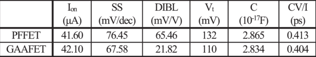
Figure 2. Characteristics of 2 tube GAAFET and PFFET under 5nm node [12]
Samsung began its 3nm process GAA chip production on June 30, 2022. [13] Samsung's press conference in Korea claimed that its Multi Bridge Channel FET (MBCFET), which is Samsung's first generation GAAFET, was under mass production. [13] As affirmed by Dr. Siyoung Choi, the President and Head of Foundry Business at Samsung Electronics, the second generation of MBCFET would bring up to 50 percent power saving, 30 percent performance improvement, and 30 percent deduction in transistor density compared to 5nm process. The first generation showcased a 45 percent power reduction, a 23 percent performance increase, and a 16 percent area saving. [13] Moreover, as their company's roadmap shows, Samsung predicts their 2nm node will be under mass production in 2025 and 1.4nm node in 2027. Furthermore, the company is willing to maintain the privilege of Moore's law through the sub 1nm era. However, once the silicon GAAFET reaches its scaling limit, suffering from an overwhelming short channel effect, post-silicon materials like carbon nanotubes, germanium, or other 2D materials may save the day. With the help of varying channel widths of MCBFET, Samsung was confident to satisfy numerous customers.
Even though GAAFET is clearly transcending FinFET, no commercial product has been officially released. Intel, IBM, and TSMC all announced that their new technology is in the risk production stage in 2021, while at this time, Samsung became the only industry that declares their product is in the process of mass production. [13] In the second quarter of 2023, Samsung is confident to indicate that the percent of yield in mass production of GAAFET is 60-70 percent in approximation and determined to stabilize the yield percentage and may send out transistor specification in the next quarter. The South Korean company takes a considerable lead in manufacturing GAAFET and plans to intensify its technology further. With the experience of mass production of the first-generation GAA chip, the company then presented that its second-generation 3nm process chip and first-generation 2nm chip will be released in 2025, which matched the timeline of other industries' first generation. [13] Therefore, as a result of advanced technology. Samsung is believed to have fascinated and attracted its previous clients, such as Apple, Nvidia, and AMD.
Aside from the transistor level specifications, it is essential to know the application of GAAFET transistors in the future. Smartphone is an example. Current smartphones use SoC, which is the highest level of integration that integrates the central processing unit (CPU), graphics processing unit (GPU), memory interfaces, and input-output (IO), compared to the conventional motherboard-based integration on the computer. Because of this integration, PPA becomes the most considerable factor, especially power consumption. If the power consumption is higher, for example, by a factor of 2, even if a lot improves other factors, the market would not accept the product because no one wants to charge the phone three or four times a day.
Based on the purpose, GAAFET technology will be more commonly used than FinFETs since it has a more extensive variety of functionality. Smartphones, televisions, personal computers, and other electronic products are all believed to have GAAFET applied to them. Digital integrated circuit design with GAAFETs is utilized as a switching devices for effective power saving and management. Moreover, according to new research, personal computers and televisions grew much faster than cell phones from 2019 to 2021 due to the global pandemic restrictions and more excellent time spent working and studying remotely at home. [14] All these electronic devices are expected to increase up to 3 percent annually starting in 2022. Therefore, the increasing demand for personal electronics further creates new opportunities for the GAAFET chip market. Based on the research, the GAAFET market is worth $30.06 million across the world, and it is expected to be worth over $470 million by 2030, which would have a compound annual growth rate of over 35 percent. [14]
4. Conclusion
With the development of manufacturing technology, GAAFETs are expected to be used in the most sophisticated chip designs in the following years. The transition between FinFET and GAAFET would be slow but steady, given that the fabrication process for GAAFET is not yet mature. Even though current industries can make 3nm chips in FinFET technology, the cost of production is relatively higher than anticipated. Additionally, with excessive leakage current and short channel effect, FinFET is struggling with further shrinking. However, GAAFET can deal with all these shortcomings. These transistors will improve the performance and power consumption of next-generation chips, such as graphics processing units, central processing units, smartphone SoCs, as well as other technologies while keeping the mass production of advanced chips at a reasonable price, thanks to their capacity to be produced at a cost that is acceptable for chipmakers. Furthermore, GAAFETs outperform earlier designs regarding PPA, current leakage, and control, making them a more sustainable and ecologically friendly solution for industries.
References
[1]. Jurczak, M., Collaert, N., Veloso, A., Hoffmann, T., & Biesemans, S. (2009) Review of FINFET technology. 2009 IEEE International SOI Conference, Foster City, pp. 1-4.
[2]. Jang, D., Yakimets, D., Eneman, G., Schuddinck, P., Bardon, M. G., Raghavan, P., ... & Mocuta, A. (2017) Device Exploration of NanoSheet Transistors for Sub-7-nm Technology Node. IEEE Transactions on Electron Devices, vol. 64, no. 6, pp. 2707-2713.
[3]. Lee, H., Yu, L. E., Ryu, S. W., Han, J. W., Jeon, K., Jang, D. Y., ... & Choi, Y. K. (2006) Sub-5nm All-Around Gate FinFET for Ultimate Scaling. 2006 Symposium on VLSI Technology, 2006. Digest of Technical Papers., Honolulu, pp. 58-59.
[4]. Das, U. K., & Bhattacharyya, T. K. (2020) Opportunities in Device Scaling for 3-nm Node and Beyond: FinFET Versus GAA-FET Versus UFET. IEEE Transactions on Electron Devices, vol. 67, no. 6, pp. 2633-2638
[5]. Yoon, J. S., Jeong, J., Lee, S., Lee, J., & Baek, R. H. (2020) Gate-All-Around FETs: Nanowire and Nanosheet Structure. IntechOpen.
[6]. Loubet, N., Hook, T., Montanini, P., Yeung, C. W., Kanakasabapathy, S., Guillom, M., ... & Khare, M. (2017) Stacked nanosheet gate-all-around transistor to enable scaling beyond FinFET. 2017 Symposium on VLSI Technology, Kyoto, pp. T230-T231.
[7]. Agha, F. N. H., Naif, Y. H., & Shakib, M. N. (2021). Review of nanosheet transistors technology. Tikrit Journal of Engineering Sciences, pp. 40-48.
[8]. Semiconductor Engineering. (2023) Gate-All-Around FET. https://semiengineering.com/knowledge_centers/integrated-circuit/transistors/3d/gate-all-around-fet/.
[9]. Lin, Y. W., Chang, H. H., Huang, Y. H., Sun, C. J., Yan, S. C., Lin, S. W., ... & Hou, F. J. (2021). Tightly Stacked 3D Diamond-Shaped Ge Nanowire Gate-All-Around FETs With Superior nFET and pFET Performance. IEEE Electron Device Letters, pp. 1727-1730
[10]. Lu, W., Xie, P., & Lieber, C. M. (2008). Nanowire transistor performance limits and applications. IEEE transactions on Electron Devices, pp. 2859-2876.
[11]. Knoedler, M., Bologna, N., Schmid, H., Borg, M., Moselund, K. E., Wirths, S., ... & Riel, H. (2017). Observation of twin-free GaAs nanowire growth using template-assisted selective epitaxy. Crystal Growth & Design, pp. 6297-6302.
[12]. Huang, Y. C., Chiang, M. H., Wang, S. J., & Fossum, J. G. (2017). GAAFET versus pragmatic FinFET at the 5nm Si-based CMOS technology node. IEEE Journal of the Electron Devices Society, pp. 164-169.
[13]. Samsung Semiconductor Global (2023) Samsung Opens the Gate to Transistor Performance, Power, and Area Improvements with MBCFET. semiconductor.samsung.com/newsroom/tech-blog/samsung-opens-the-gate-to-transistor-performance-power-and-area-improvements-with-mbcfet/.
[14]. Strategic Market Research. (2022) Gate-All-Around FET Technology Market 2021-2030. https://www.strategicmarketresearch.com/market-report/-gaafet-technology-market.
Cite this article
Jiang,Y. (2024). Introduction and commercial prospect of GAAFET . Applied and Computational Engineering,30,224-229.
Data availability
The datasets used and/or analyzed during the current study will be available from the authors upon reasonable request.
Disclaimer/Publisher's Note
The statements, opinions and data contained in all publications are solely those of the individual author(s) and contributor(s) and not of EWA Publishing and/or the editor(s). EWA Publishing and/or the editor(s) disclaim responsibility for any injury to people or property resulting from any ideas, methods, instructions or products referred to in the content.
About volume
Volume title: Proceedings of the 2023 International Conference on Machine Learning and Automation
© 2024 by the author(s). Licensee EWA Publishing, Oxford, UK. This article is an open access article distributed under the terms and
conditions of the Creative Commons Attribution (CC BY) license. Authors who
publish this series agree to the following terms:
1. Authors retain copyright and grant the series right of first publication with the work simultaneously licensed under a Creative Commons
Attribution License that allows others to share the work with an acknowledgment of the work's authorship and initial publication in this
series.
2. Authors are able to enter into separate, additional contractual arrangements for the non-exclusive distribution of the series's published
version of the work (e.g., post it to an institutional repository or publish it in a book), with an acknowledgment of its initial
publication in this series.
3. Authors are permitted and encouraged to post their work online (e.g., in institutional repositories or on their website) prior to and
during the submission process, as it can lead to productive exchanges, as well as earlier and greater citation of published work (See
Open access policy for details).
References
[1]. Jurczak, M., Collaert, N., Veloso, A., Hoffmann, T., & Biesemans, S. (2009) Review of FINFET technology. 2009 IEEE International SOI Conference, Foster City, pp. 1-4.
[2]. Jang, D., Yakimets, D., Eneman, G., Schuddinck, P., Bardon, M. G., Raghavan, P., ... & Mocuta, A. (2017) Device Exploration of NanoSheet Transistors for Sub-7-nm Technology Node. IEEE Transactions on Electron Devices, vol. 64, no. 6, pp. 2707-2713.
[3]. Lee, H., Yu, L. E., Ryu, S. W., Han, J. W., Jeon, K., Jang, D. Y., ... & Choi, Y. K. (2006) Sub-5nm All-Around Gate FinFET for Ultimate Scaling. 2006 Symposium on VLSI Technology, 2006. Digest of Technical Papers., Honolulu, pp. 58-59.
[4]. Das, U. K., & Bhattacharyya, T. K. (2020) Opportunities in Device Scaling for 3-nm Node and Beyond: FinFET Versus GAA-FET Versus UFET. IEEE Transactions on Electron Devices, vol. 67, no. 6, pp. 2633-2638
[5]. Yoon, J. S., Jeong, J., Lee, S., Lee, J., & Baek, R. H. (2020) Gate-All-Around FETs: Nanowire and Nanosheet Structure. IntechOpen.
[6]. Loubet, N., Hook, T., Montanini, P., Yeung, C. W., Kanakasabapathy, S., Guillom, M., ... & Khare, M. (2017) Stacked nanosheet gate-all-around transistor to enable scaling beyond FinFET. 2017 Symposium on VLSI Technology, Kyoto, pp. T230-T231.
[7]. Agha, F. N. H., Naif, Y. H., & Shakib, M. N. (2021). Review of nanosheet transistors technology. Tikrit Journal of Engineering Sciences, pp. 40-48.
[8]. Semiconductor Engineering. (2023) Gate-All-Around FET. https://semiengineering.com/knowledge_centers/integrated-circuit/transistors/3d/gate-all-around-fet/.
[9]. Lin, Y. W., Chang, H. H., Huang, Y. H., Sun, C. J., Yan, S. C., Lin, S. W., ... & Hou, F. J. (2021). Tightly Stacked 3D Diamond-Shaped Ge Nanowire Gate-All-Around FETs With Superior nFET and pFET Performance. IEEE Electron Device Letters, pp. 1727-1730
[10]. Lu, W., Xie, P., & Lieber, C. M. (2008). Nanowire transistor performance limits and applications. IEEE transactions on Electron Devices, pp. 2859-2876.
[11]. Knoedler, M., Bologna, N., Schmid, H., Borg, M., Moselund, K. E., Wirths, S., ... & Riel, H. (2017). Observation of twin-free GaAs nanowire growth using template-assisted selective epitaxy. Crystal Growth & Design, pp. 6297-6302.
[12]. Huang, Y. C., Chiang, M. H., Wang, S. J., & Fossum, J. G. (2017). GAAFET versus pragmatic FinFET at the 5nm Si-based CMOS technology node. IEEE Journal of the Electron Devices Society, pp. 164-169.
[13]. Samsung Semiconductor Global (2023) Samsung Opens the Gate to Transistor Performance, Power, and Area Improvements with MBCFET. semiconductor.samsung.com/newsroom/tech-blog/samsung-opens-the-gate-to-transistor-performance-power-and-area-improvements-with-mbcfet/.
[14]. Strategic Market Research. (2022) Gate-All-Around FET Technology Market 2021-2030. https://www.strategicmarketresearch.com/market-report/-gaafet-technology-market.