


1 Introduction
SiC MOSFET power devices, as typical devices of wide-bandgap semiconductor power devices, have performance advantages such as wider bandgap width, higher breakdown electric field, higher thermal conductivity, and greater saturated electron migration rate compared to Si MOSFET power devices [1]. These advantages make power supply modules prepared based on SiC MOSFET power devices have smaller size, stronger high-temperature resistance, and higher operating frequency, giving them a strong competitive edge in the aerospace power field [2]. However, SiC MOSFET power devices are affected by radiation and exhibit total dose effects during aerospace applications [3-6].
The total dose causes changes in the static and dynamic characteristics of SiC MOSFET power devices. The static characteristics of SiC MOSFET power devices include transfer characteristics, breakdown characteristics, and output characteristics, while the dynamic characteristics include capacitance characteristics, switching characteristics, short-circuit characteristics, and avalanche characteristics, etc. Currently, a large number of literatures have studied the total dose effects on the static characteristics of devices [7-11]. Only a few literatures have studied the influence of total dose on the dynamic characteristics of SiC MOSFET power devices, including the effects on capacitance characteristics and switching characteristics [11-13]. At present, there are no reports on the influence of total dose on the short-circuit and avalanche characteristics of SiC MOSFET power devices. However, under normal circumstances, the short-circuit and avalanche characteristics of SiC MOSFET power devices are weaker than those of Si MOSFET power devices. Gonzalez J O and others compared experimentally and found that Si MOSFET power devices have better short-circuit time and avalanche time than SiC MOSFET power devices [14].
This paper studies the degradation patterns and mechanisms of the short-circuit and avalanche characteristics of SiC MOSFET power devices under total dose through experiments and simulations, which is divided into two parts. The first part studies the degradation patterns of the short-circuit and avalanche characteristics of SiC MOSFET power devices, and the second part analyzes these degradation patterns theoretically and through simulation.
2 Test samples and test system
The device samples studied in this paper for the dynamic characteristics of SiC MOSFET power devices under total dose are flat-structure SiC MOSFET power device samples from CREE Company, with plastic encapsulation and a rated breakdown voltage of 1200V, as shown in Figure 1. The total dose test was irradiated using a cobalt-60 gamma-ray source from the China Metrology Institute, with a dose rate of 50rad (Si)/s. The total dose effect of the SiC MOSFET power devices studied in this paper was tested under the cobalt-60 radiation source using an on-state bias condition, with a bias voltage of 15V for the gate-source voltage and 0V for the drain-source voltage. The devices were first irradiated in the cobalt-60 radiation environment. After reaching a certain cumulative dose under the on-state radiation bias condition, they were removed from the cobalt-60 radiation source and the electrical characteristics were tested in the room temperature test area.
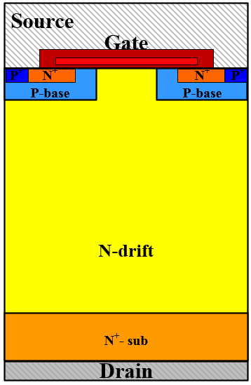
Figure 1. Schematic cross-sectional view of SiC MOSFET power devices
Studying the influence of total dose on the short-circuit characteristics and avalanche characteristics of SiC MOSFET power devices requires the establishment of a characterization system for these device characteristics. Figure 2 illustrates the schematic and testing system diagram for the short-circuit test of SiC MOSFET, where Figure 2(a) is the principal diagram of the short-circuit test, and Figure 2(b) is the physical system diagram of the short-circuit test. By controlling the drive voltage applied to the device's gate-source, the device can operate under short-circuit conditions, and the theoretical waveform is shown in Figure 3. A drive voltage VGS with a pulse width of t2-t0 is applied across the gate-source terminals of the device; from t0 to t1, the current through the device rises to the short-circuit peak current, and then enters saturation during the t1-t2 period. If the device can be reliably turned off after the short circuit, the energy dissipated during this process is defined as the short-circuit energy Esc. Its magnitude can be calculated by integrating the current through the device's drain-source terminals and the voltage across them, as shown in Equation (1):
\( E_{sc}=\int_{t0}^{t2}I_{ds}V_{ds}dt \) (1)
If the short-circuit time of the device is continuously increased, the last complete short-circuit process that the device undergoes (before) when it fails due to a short circuit is the short-circuit tolerance energy.
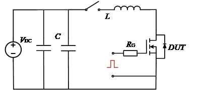
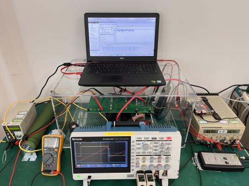
The schematic and testing platform diagram of the Unclamped Inductive Switching (UIS) test circuit for the avalanche capability of SiC MOSFET without clamping are shown in Figure 4, where Figure 4(a) is the principal diagram of the UIS test, and Figure 4(b) is the physical platform diagram of the UIS test. By controlling the drive voltage applied to the device's gate-source, the device can operate in the UIS state, and the theoretical waveform is shown in Figure 5. During the time t0-t1, under the action of the inductor, the current through the device's drain-source terminals increases linearly; at time t1, the device is turned off, and the loop current undergoes avalanche breakdown through the device's body diode, releasing the energy stored in the inductor. Figure 5 shows the theoretical waveform of the UIS test for the device; when the energy can be completely dissipated, the test waveform is as shown by the solid line; otherwise, the test device fails due to avalanche, and the test waveform is as shown by the dashed line. The energy dissipated in the last event before the device fails due to avalanche is defined as the device's avalanche tolerance (EAS). Generally, the avalanche tolerance of the device can be calculated using Equation (2):
\( E_{AS}=\frac{1}{2}LI_{peak}^{2}V_{br}/(V_{br}-V_{DC}) \) (2)
where Ipeak is the peak avalanche current of the device, L is the inductance of the loop, Vbr is the avalanche breakdown voltage of the device, and VDC is the bus voltage.
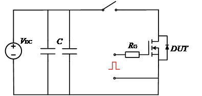
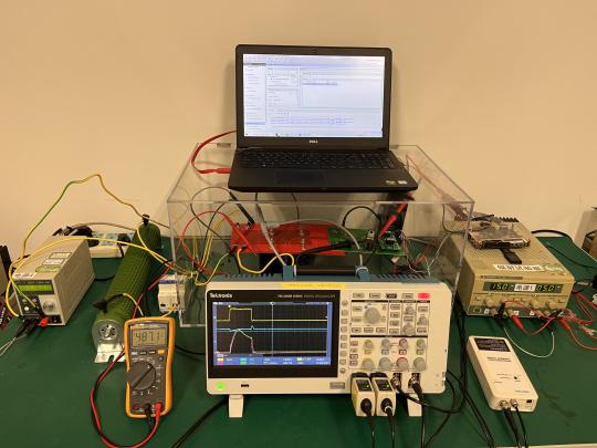
Figure 2. Short circuit test system. (a) The schematic of short circuit test circuit and (b) the picture of short circuit test system
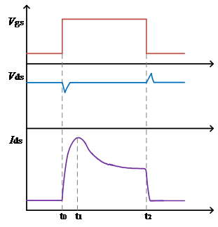
Figure 3. Short circuit theoretical waveforms
(a) (b)
Figure 4. UIS test platform. (a) The schematic of UIS test circuit and (b) the picture of UIS test platform
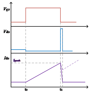
Figure 5. UIS theoretical waveforms
3 Degradation patterns of dynamic characteristics of SiC MOSFET power devices
3.1 Degradation pattern of short-circuit characteristics
Figure 6 shows the typical waveform diagram of the 600V short-circuit gate-source failure for a 1200V SiC MOSFET power device, where the black, blue, and red curves represent the device's drain-source voltage VDS, drain-source current IDS, and gate-source voltage VGS, respectively. It can be observed from the figure that at t=0s, VGS rises to the gate turn-on voltage, IDS initially slowly increases to the short-circuit peak current IDS=210A, then gradually decreases to the saturation current IDS=119A; at t=5.5µs, VGS drops to the gate turn-off voltage, at which point IDS rapidly decreases, but the device does not fully turn off, and the gate-source leakage current IDS slowly decreases from 28A; around t=8.2µs, VGS suddenly increases, and the device experiences a gate-source short circuit. Under different total doses, the failure mode of the SiC MOSFET planar structure device at 600V is consistently a gate-source failure, with the gate-source equivalent resistance measured by a multimeter ranging from a few ohms to thousands of ohms after the device fails due to a short circuit.
Figure 7 illustrates the relationship between the short-circuit tolerance time and short-circuit tolerance energy of the SiC MOSFET power device with the total dose. It can be seen from the figure that as the total dose increases from 0 to 600krad (Si), there is a noticeable decrease in the device's short-circuit tolerance, where the short-circuit tolerance time decreases from 5.6µs to 4.6µs, and the corresponding short-circuit tolerance energy decreases from 471mJ to 406mJ, a reduction of 13.8%. However, when the total dose is relatively small (300krad (Si)), the reduction in both short-circuit tolerance time and energy does not exceed 5%.
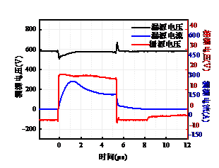
Figure 6. Measured short circuit waveforms of planar SiC MOSFET power devices
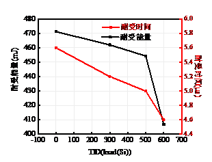
Figure 7. Calculated SCWE and SCWT of planar SiC MOSFET before and after irradiation
3.2 Degradation Pattern of Avalanche Characteristics
Figure 8 illustrates the typical waveform of avalanche failure for a 1200V SiC MOSFET power device, where the black and red curves represent the device's drain-source voltage VDS and drain-source current IDS, respectively. From Figure 8, it can be observed that at t=0µs, the device is turned on, and IDS rises linearly; at t=825µs, the device is turned off, and avalanche breakdown occurs, causing VDS to rapidly increase to the device's breakdown voltage value (slightly higher than the actual breakdown voltage of the device). At this point, the energy stored in the inductor is released through the circuit formed with the MOSFET; subsequently, the device fails thermally as it cannot completely dissipate the energy stored in the inductor.
Figure 9 shows the relationship between the avalanche tolerance of the SiC MOSFET power device and the total dose. It can be seen from Figure 9 that as the total dose accumulates from 0 to 600krad (Si), the device's avalanche tolerance energy decreases from 679mJ to 507mJ, a reduction of 25.2%.
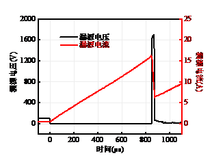
Figure 8. Typical avalanche current and voltage waveforms for unclamped inductive switching (UIS) test.
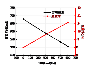
Figure 9. Calculated avalanche energy and change rate of SiC MOSFET power devices before and after irradiation
4 Degradation Mechanism of the Dynamic Characteristics of SiC MOSFET Power Devices
Total dose generates oxide trap charges and interface state charges in the gate oxide of SiC MOSFET power devices. These trap charges cause the transfer characteristics of the device to shift negatively, where oxide trap charges are the main factor leading to the negative shift in the device's transfer characteristics. Trap charges induced by radiation affect the robustness of the device, thereby impacting the device's short-circuit and avalanche tolerance capabilities.
4.1 Mechanism of Short-Circuit Characteristic Degradation
After being subjected to radiation, the short-circuit tolerance time of the device decreases significantly, and the lattice temperature is higher than the lattice temperature before the device was irradiated. Based on the above analysis, it can be concluded that the main reason for the rapid decrease in the device's short-circuit tolerance energy and time under high dose level conditions is the severe defects produced in the device's oxide by higher dose radiation.
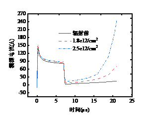
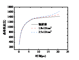
To further study the impact of total dose on the short-circuit tolerance characteristics of SiC MOSFET power devices, this paper established a two-dimensional TCAD simulation model of SiC MOSFET power devices and added trap charges to the gate oxide of the device, with charge densities of Not_Gox=1.8×10^12/cm^2 and Not_Gox=2.5×10^12/cm^2. Figures 10(a) and 10(b) show the simulation results of the drain-source current and lattice temperature of the SiC MOSFET power device before and after radiation, respectively. From Figure 10(a), it can be seen that the device failed at a short-circuit time of 7µs after being irradiated; whereas, it did not fail at the same short-circuit time before being irradiated. As the radiation dose accumulates, the degree of failure at a short-circuit time of 7µs becomes more severe. Figure 10(b) shows the lattice temperature of the device during short-circuit conditions before and after radiation. At a short-circuit time of 20µs, the lattice temperature of the device gradually increases.
(a) (b)
Figure 10. Simulated (a) drain current waveforms and (b) lattice temperature waveforms of planar SiC MOSFET power devices before and after irradiation with Not_GOX=1.8×10¹²/cm2 and 2.5×10¹²/cm2.
4.2 Degradation Pattern of Avalanche Characteristics
The trap charges induced in the oxide by radiation are the primary cause of the reduction in the avalanche tolerance energy of the device. To further investigate the impact of total dose on the avalanche tolerance characteristics of SiC MOSFET power devices, this paper has established a two-dimensional TCAD simulation model for SiC MOSFET power devices and added trap charges to the gate oxide of the devices, with charge densities of Not_Gox=1.4×10^12/cm^2 and Not_Gox=1.8×10^12/cm^2. Figure 11 presents the simulation results of the drain-source current for the SiC MOSFET power devices before and after radiation. It can be observed from Figure 11 that when the charge density is Not_Gox=1.8×10^12/cm^2, the SiC MOSFET power device exhibited a leakage current during the turn-off process, leading to failure. In contrast, when not subjected to radiation and when subjected to radiation with a charge density of Not_Gox=1.4×10^12/cm^2, the device did not produce a leakage current during turn-off and could turn off normally.
Figure 11 also displays the simulation results of the lattice temperature for the SiC MOSFET power devices. It can be seen from Figure 11 that when the charge density is Not_Gox=1.8×10^12/cm^2, the maximum lattice temperature of the device is around 1100K. However, when not subjected to radiation and when subjected to radiation with a charge density of Not_Gox=1.4×10^12/cm^2, the maximum lattice temperature of the device is only 1050K.
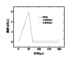
Figure 11. The simulated drain-source current waveforms of SiC MOSFET power devices before and after irradiation with Not_GOX=1.4×10¹²/cm2 and 1.8×10¹²/cm2.
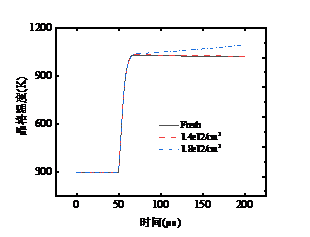
Figure 12. The simulated lattice temperature of SiC MOSFET power devices before and after irradiation with Not_GOX=1.4×10¹²/cm2 and 1.8×10¹²/cm2.
5 Conclusion
This paper investigates the impact of total dose on the short-circuit and avalanche characteristics of SiC MOSFET power devices through radiation testing. The study found that after being subjected to radiation, the devices exhibited a noticeable degradation in both short-circuit tolerance and avalanche tolerance. Theoretical and simulation analyses revealed that the main reason for the degradation of the short-circuit and avalanche tolerance after radiation exposure is the generation of trap charges in the oxide due to the total dose. These research findings enhance the understanding of potential risks encountered by aerospace power circuit designers when SiC MOSFET power devices operate in a space environment, and they also provide technical support for the application of SiC MOSFET power devices in aerospace power systems.
References
[1]. Boomerk, Lauenstein, J. M., & Hammouda. (2016). Body of knowledge for silicon carbide power electronics [R]. NASA, USA.
[2]. Kimoto, T. (2013). Ultrahigh-voltage SiC devices for future power infrastructure. In 2013 Proceedings of the European, Bucharest, Romania, pp. 22-29.
[3]. Popelka, S., & Hazdra, P. (2016). Effect of electron irradiation on 1700V 4H-SiC MOSFET characteristics. In Materials Science Forum, Switzerland, pp. 856-859.
[4]. Lauenstein, J. M., Casey, M. C., Ladbury, R. L., et al. (2021). Space radiation effects on SiC power device reliability. In 2021 IEEE International Reliability Physics Symposium (IRPS), Monterey, CA, USA, pp. 1-8.
[5]. Adell, P., & Scheick, L. (2013). Radiation effects in power systems: A review. IEEE Transactions on Nuclear Science, 60(3), 1929-1952.
[6]. Sun, Y., Wan, X., Liu, Z., et al. (2022). Investigation of total ionizing dose effects in 4H-SiC power MOSFET under gamma ray radiation. Radiation Physics And Chemistry, 197(110219).
[7]. Hazdra, P., & Popelka, S. (2019). Displacement damage and total ionization dose effects on 4H-SiC power devices. IET Power Electronics, 12, 3910-3918.
[8]. Hu, D., Zhang, J., Jia, Y., et al. (2018). Impact of different gate biases on irradiation and annealing responses of SiC MOSFETs. IEEE Transactions on Electron Devices, 65, 3719-3724.
[9]. Krishnamurthy, S., Kannan, R., Kiong, C. C., Ibrahim, T. B., & Abdullah, Y. (2019). Impact of gamma-ray irradiation on dynamic characteristics of Si and SiC power MOSFETs. International Journal of Electrical and Computer Engineering Science, 9, 1453-1460.
[10]. Akturk, A., McGarrity, J. M., Potbhare, S., et al. (2012). Radiation effects in commercial 1200V 24A silicon carbide power MOSFETs. IEEE Transactions on Nuclear Science, 59, 3258-3264.
[11]. Feng, H., Yang, S., Liang, X., et al. (2021). Radiation effects and mechanisms on switching characteristics of silicon carbide power MOSFETs. Journal of Nanoelectronics and Optoelectronics, 16, 1423-1429.
[12]. Akturk, A., et al. (2012). Radiation effects in commercial 1200V 24A silicon carbide power MOSFETs. IEEE Transactions on Nuclear Science, 59(6), 3258-3264.
[13]. Godignon, P., Massetti, S., Jordà, X., et al. (2016). SiC power switches evaluation for space applications requirements. Materials Science Forum, 858, 852-855.
[14]. Envelope, J., Ad, A., Eb, A., et al. (2022). Benchmarking the robustness of Si and SiC MOSFETs: Unclamped inductive switching and short-circuit performance. Microelectronics Reliability.
Cite this article
Chen,M.;Zhang,L.;Sun,X.;Li,Z.;Sui,C. (2024). Research on the influence of total dose on the short-circuit and avalanche characteristics of SiC MOSFET power devices. Advances in Engineering Innovation,11,24-30.
Data availability
The datasets used and/or analyzed during the current study will be available from the authors upon reasonable request.
Disclaimer/Publisher's Note
The statements, opinions and data contained in all publications are solely those of the individual author(s) and contributor(s) and not of EWA Publishing and/or the editor(s). EWA Publishing and/or the editor(s) disclaim responsibility for any injury to people or property resulting from any ideas, methods, instructions or products referred to in the content.
About volume
Journal:Advances in Engineering Innovation
© 2024 by the author(s). Licensee EWA Publishing, Oxford, UK. This article is an open access article distributed under the terms and
conditions of the Creative Commons Attribution (CC BY) license. Authors who
publish this series agree to the following terms:
1. Authors retain copyright and grant the series right of first publication with the work simultaneously licensed under a Creative Commons
Attribution License that allows others to share the work with an acknowledgment of the work's authorship and initial publication in this
series.
2. Authors are able to enter into separate, additional contractual arrangements for the non-exclusive distribution of the series's published
version of the work (e.g., post it to an institutional repository or publish it in a book), with an acknowledgment of its initial
publication in this series.
3. Authors are permitted and encouraged to post their work online (e.g., in institutional repositories or on their website) prior to and
during the submission process, as it can lead to productive exchanges, as well as earlier and greater citation of published work (See
Open access policy for details).
References
[1]. Boomerk, Lauenstein, J. M., & Hammouda. (2016). Body of knowledge for silicon carbide power electronics [R]. NASA, USA.
[2]. Kimoto, T. (2013). Ultrahigh-voltage SiC devices for future power infrastructure. In 2013 Proceedings of the European, Bucharest, Romania, pp. 22-29.
[3]. Popelka, S., & Hazdra, P. (2016). Effect of electron irradiation on 1700V 4H-SiC MOSFET characteristics. In Materials Science Forum, Switzerland, pp. 856-859.
[4]. Lauenstein, J. M., Casey, M. C., Ladbury, R. L., et al. (2021). Space radiation effects on SiC power device reliability. In 2021 IEEE International Reliability Physics Symposium (IRPS), Monterey, CA, USA, pp. 1-8.
[5]. Adell, P., & Scheick, L. (2013). Radiation effects in power systems: A review. IEEE Transactions on Nuclear Science, 60(3), 1929-1952.
[6]. Sun, Y., Wan, X., Liu, Z., et al. (2022). Investigation of total ionizing dose effects in 4H-SiC power MOSFET under gamma ray radiation. Radiation Physics And Chemistry, 197(110219).
[7]. Hazdra, P., & Popelka, S. (2019). Displacement damage and total ionization dose effects on 4H-SiC power devices. IET Power Electronics, 12, 3910-3918.
[8]. Hu, D., Zhang, J., Jia, Y., et al. (2018). Impact of different gate biases on irradiation and annealing responses of SiC MOSFETs. IEEE Transactions on Electron Devices, 65, 3719-3724.
[9]. Krishnamurthy, S., Kannan, R., Kiong, C. C., Ibrahim, T. B., & Abdullah, Y. (2019). Impact of gamma-ray irradiation on dynamic characteristics of Si and SiC power MOSFETs. International Journal of Electrical and Computer Engineering Science, 9, 1453-1460.
[10]. Akturk, A., McGarrity, J. M., Potbhare, S., et al. (2012). Radiation effects in commercial 1200V 24A silicon carbide power MOSFETs. IEEE Transactions on Nuclear Science, 59, 3258-3264.
[11]. Feng, H., Yang, S., Liang, X., et al. (2021). Radiation effects and mechanisms on switching characteristics of silicon carbide power MOSFETs. Journal of Nanoelectronics and Optoelectronics, 16, 1423-1429.
[12]. Akturk, A., et al. (2012). Radiation effects in commercial 1200V 24A silicon carbide power MOSFETs. IEEE Transactions on Nuclear Science, 59(6), 3258-3264.
[13]. Godignon, P., Massetti, S., Jordà, X., et al. (2016). SiC power switches evaluation for space applications requirements. Materials Science Forum, 858, 852-855.
[14]. Envelope, J., Ad, A., Eb, A., et al. (2022). Benchmarking the robustness of Si and SiC MOSFETs: Unclamped inductive switching and short-circuit performance. Microelectronics Reliability.