


1. Introduction
With the rapid development of modern wireless communication technologies, the millimeter-wave (mmWave) frequency band (30–300 GHz) has garnered increasing attention due to its abundant spectral resources. mmWave communication offers high data rates, large bandwidth, and narrow beams, demonstrating significant potential in fields such as 5G communications, radar systems, and satellite communications [1-3]. However, the electromagnetic propagation characteristics of mmWave bands impose stringent demands on antenna design, including miniaturization, high precision, and a high degree of integration. Traditional silicon-based antennas typically adopt rectangular chip structures, resulting in relatively large footprints. This poses integration challenges within high-density wafer-level system-in-package (WLSiP) technologies. Moreover, conventional antennas are often fabricated separately on substrates and integrated via interface connectors, which can introduce substantial parasitic parameters and losses. These issues reduce process consistency and limit the performance improvement of antennas in mmWave systems.
This paper proposes a novel second-order fractal antenna for mmWave applications, which achieves miniaturization, high performance, and seamless integration with other devices through innovative structural and process design. The antenna is suitable for silicon-based 3D integrated structures, enhancing system-level integration and overall performance. It offers critical technical support for the widespread application of mmWave technologies across various domains.
2. Structural design of the millimeter-wave second-order fractal antenna
2.1. Overall structural design
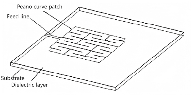
The millimeter-wave second-order fractal antenna primarily consists of a substrate, seed layers, a BCB (Benzo Cyclo Butene) dielectric layer, and a conductive layer. The first seed layer is sputtered onto the bottom of the substrate. The top surface is spin-coated with the BCB dielectric layer, which is then cured. A second seed layer is sputtered on top of the BCB layer, forming a connection with the conductive layer above it. The conductive layer features a Peano curve pattern.
The substrate is made of double-side-polished high-resistivity silicon, with a thickness ranging from 300 to 450 μm. This type of silicon offers excellent mechanical stability, thermal conductivity, and electrical properties, providing a robust physical foundation for the antenna. It is also compatible with subsequent fabrication steps, which facilitates the realization of high-performance antenna manufacturing. Both seed layers consist of a titanium-tungsten (TiW) layer and a copper (Cu) layer. The TiW layer has a thickness of 450–550 nm, and the Cu layer ranges from 1800 to 2200 nm in thickness. The TiW layer enhances the adhesion between the seed layer and the substrate. During the sputtering process, the TiW layer is deposited prior to the Cu layer and has strong chemical affinity with the substrate material, enabling firm chemical bonding. This ensures the stable attachment of the Cu layer to the substrate or the BCB dielectric layer throughout subsequent processing steps, providing a reliable base for the deposition of the conductive metal layer. The conductive layer is made of copper due to its excellent electrical conductivity, which effectively reduces resistive losses during signal transmission and enhances the radiation efficiency of the antenna. Moreover, copper is well-established in microfabrication processes, allowing for precise patterning and electroplating to form the desired Peano curve and transmission line structures.
2.2. Application of the Peano curve
The Peano curve is a type of fractal curve that, in the limiting case, can fill an entire rectangular area. At a macroscopic level, it functions similarly to a rectangular patch. However, due to its intricate and winding geometry, it has a significantly longer physical length while occupying less surface area compared to conventional rectangular patches [4,5]. This unique geometric characteristic enables the antenna to accommodate a longer current path within a limited space, thereby optimizing its electromagnetic performance.
In the millimeter-wave second-order fractal antenna, a second-order Peano curve replaces the traditional rectangular patch, altering the current path to become more meandering, as illustrated in Figure 1. According to antenna resonance principles, increasing the current path length—while keeping other parameters unchanged—can reduce the physical size of the patch while maintaining the same resonant frequency. This design approach not only achieves antenna miniaturization but also enhances performance indicators such as bandwidth and gain, making it well-suited for the requirements of the millimeter-wave frequency band.
3. Fabrication design of the millimeter-wave second-order fractal antenna
3.1. Process flow design
3.1.1. Substrate preparation
High-resistivity double-side-polished silicon wafers are selected as substrates. Before subsequent processing steps, the substrate surface must be clean, flat, and free of contaminants or defects. Strict substrate screening and pretreatment ensure an ideal foundation for seed layer sputtering and dielectric layer coating, thereby ensuring high quality and performance in antenna fabrication.
3.1.2. Seed layer sputtering
Magnetron sputtering is employed to deposit the first seed layer on the underside of the substrate. This technique offers high deposition rates, excellent film quality, and strong process repeatability, enabling precise control over the thickness and uniformity of the TiW and Cu layers. A TiW layer is first sputtered onto the substrate bottom, with a thickness adjustable between 450–550 nm depending on design requirements. A Cu layer is then sputtered on top of the TiW layer, with thickness controlled within the range of 1800–2200 nm. During sputtering, key parameters such as power, pressure, and temperature are precisely regulated to ensure strong adhesion between the seed layer and the substrate, while also achieving the desired crystalline and electrical properties of the seed layers to meet antenna design specifications.
3.1.3. BCB dielectric layer coating and curing
The substrate is preheated in an oven for 1.5 to 2 minutes. Immediately afterward, a BCB-specific adhesion promoter is spin-coated onto the substrate. A thick-film coater is used to apply the BCB layer, with coating speed and duration carefully controlled to ensure flatness and edge coverage. A reflow oven is used to cure the BCB layer, employing a multi-step temperature ramp to prevent cracking during curing. This results in a high-thickness, mechanically stable BCB dielectric layer.
3.1.4. Pattern formation: photolithography and electroplating
A second seed layer is sputtered onto the cured BCB dielectric layer, followed by spin-coating of photoresist. The Peano curve and transmission line patterns are defined via photolithographic exposure and development. Electroplating is then performed on the exposed areas of the second seed layer to form the conductive layer. The remaining unexposed photoresist is removed to reveal the underlying seed layer. Ion beam etching is subsequently used to remove the unpatterned second seed layer on the substrate surface. The etching depth must be sufficient to fully remove this layer. At this point, the complete antenna structure is fabricated.
3.2. Analysis of process innovation
This fabrication process enables wafer-level batch production, significantly enhancing manufacturing efficiency and reducing the cost per antenna. The multilayer thin-film design on both sides of the wafer also mitigates warpage issues commonly associated with single-sided integration, thereby improving mechanical stability and structural reliability. Additionally, the materials and processes used are compatible with other device and chip manufacturing steps, facilitating seamless integration with other circuits and components. This compatibility reduces reliability risks caused by process mismatches and supports the continued miniaturization and high integration of millimeter-wave systems.
4. Conclusion
This study presented the design and fabrication of a millimeter-wave second-order fractal antenna. Structurally, the use of fractal curves enabled antenna miniaturization by significantly reducing patch size while maintaining resonance frequency and performance. In terms of fabrication, the process allows for wafer-level batch production, which not only reduces cost but also addresses substrate warpage, improving both mechanical stability and process compatibility. Looking ahead, further optimization of antenna structures and fabrication techniques could enhance performance even more. Additionally, research into the antenna’s adaptability in complex scenarios and diverse applications will support the advancement of millimeter-wave technology in fields such as intelligent transportation, the Internet of Things (IoT), satellite communications, and medical electronics.
Funded project
Shanghai Science and Technology Committee (23141901100)
References
[1]. Lin, P., Gao, Y. H., Feng, W. J. (2025). Design of a W-band T/R Module with Silicon-based 3D Heterogeneous Integration Technology.Telecommunication Technology,65(4), 608-612.
[2]. Yang, Z. & Ma, K. X. (2024). Research on silicon-based millimeter-wave terahertz frequency multiplier.Space Electronic Technology,21(4), 9-13.
[3]. Hong, W., Chen, Z., Zhou, P. G., Chen, J. X., Peng, Z. G. & Wang, Z. J. (2023). Millimeter Wave and Terahertz Integrated Circuits and Process,Journal of Microwaves,39(5), 1-4.
[4]. Wang, G., Zhao, X. R., Yin, Y. H., Xia, C. H., Zhou, C. J., Yuan, Y. & Wang, C. Q. (2023). Antenna Design Based on Fractal Structure and Fabrication of an Antenna-Chip Integrated RF Module,Electronics & Packaging,23(8), 1-9.
[5]. Wu, G. H., Ke, Y. B., Zhang, L. & Tao, M. (2022). Sub-wavelength scale acoustic metamaterial based on Peano fractal,Journal of Vibration and Shock,41(23), 230-239.
Cite this article
Zhou,Y.;Wu,Z. (2025). Process design of a millimeter-wave second-order fractal antenna and its applications in three-dimensional integration. Advances in Engineering Innovation,16(7),177-179.
Data availability
The datasets used and/or analyzed during the current study will be available from the authors upon reasonable request.
Disclaimer/Publisher's Note
The statements, opinions and data contained in all publications are solely those of the individual author(s) and contributor(s) and not of EWA Publishing and/or the editor(s). EWA Publishing and/or the editor(s) disclaim responsibility for any injury to people or property resulting from any ideas, methods, instructions or products referred to in the content.
About volume
Journal:Advances in Engineering Innovation
© 2024 by the author(s). Licensee EWA Publishing, Oxford, UK. This article is an open access article distributed under the terms and
conditions of the Creative Commons Attribution (CC BY) license. Authors who
publish this series agree to the following terms:
1. Authors retain copyright and grant the series right of first publication with the work simultaneously licensed under a Creative Commons
Attribution License that allows others to share the work with an acknowledgment of the work's authorship and initial publication in this
series.
2. Authors are able to enter into separate, additional contractual arrangements for the non-exclusive distribution of the series's published
version of the work (e.g., post it to an institutional repository or publish it in a book), with an acknowledgment of its initial
publication in this series.
3. Authors are permitted and encouraged to post their work online (e.g., in institutional repositories or on their website) prior to and
during the submission process, as it can lead to productive exchanges, as well as earlier and greater citation of published work (See
Open access policy for details).
References
[1]. Lin, P., Gao, Y. H., Feng, W. J. (2025). Design of a W-band T/R Module with Silicon-based 3D Heterogeneous Integration Technology.Telecommunication Technology,65(4), 608-612.
[2]. Yang, Z. & Ma, K. X. (2024). Research on silicon-based millimeter-wave terahertz frequency multiplier.Space Electronic Technology,21(4), 9-13.
[3]. Hong, W., Chen, Z., Zhou, P. G., Chen, J. X., Peng, Z. G. & Wang, Z. J. (2023). Millimeter Wave and Terahertz Integrated Circuits and Process,Journal of Microwaves,39(5), 1-4.
[4]. Wang, G., Zhao, X. R., Yin, Y. H., Xia, C. H., Zhou, C. J., Yuan, Y. & Wang, C. Q. (2023). Antenna Design Based on Fractal Structure and Fabrication of an Antenna-Chip Integrated RF Module,Electronics & Packaging,23(8), 1-9.
[5]. Wu, G. H., Ke, Y. B., Zhang, L. & Tao, M. (2022). Sub-wavelength scale acoustic metamaterial based on Peano fractal,Journal of Vibration and Shock,41(23), 230-239.