


1. Introduction
Photonic Crystals (PhCs), as an artificial periodic dielectric structure material, achieve precise control over the propagation path of electromagnetic waves by regulating the Photonic Bandgap (PBG), and exhibit important application value in fields such as optical communication, quantum optics, and integrated photonic chips [1]. As a core functional unit of photonic crystals, point defect microcavities form light field localization characteristics through local permittivity perturbation, which can enhance the interaction between light and matter at the subwavelength scale, serving as a key foundation for high-performance devices such as microcavity lasers and optical filters. However, their design process relies on complex electromagnetic simulation and parameter optimization, and the computational efficiency and precision bottlenecks of traditional methods urgently need to be broken. Specifically, traditional design requires optimization through a trial-and-error process of "parameter scanning-simulation verification-iterative adjustment". A single full-band band structure simulation requires a time investment ranging from hours to days, while the computational burden grows exponentially under multi-parameter coupling—posing challenges for meeting the engineering demands of rapid development in high-performance photonic devices [2].
Existing photonic crystal microcavity designs primarily depend on numerical simulation techniques such as the Finite-Difference Time-Domain (FDTD) method and the Plane Wave Expansion Method (PWEM), realizing structural optimization via parameter scanning [3]. Such methods have three limitations: first, high computational cost, where a single full-band band structure simulation takes hours to days, and the computational load grows exponentially in multi-parameter optimization; second, insufficient global optimization capability, making it difficult to achieve the global optimal solution for device performance (such as quality factor Q and mode volume) under the coupling of multiple physical parameters; third, long design cycles, relying on the repeated iterative process of "trial-and-error-simulation-adjustment", which cannot meet the needs of rapid engineering design..
In recent years, data-driven intelligent design methods have gradually become a research hotspot in this field [4]. For instance, inverse design frameworks based on machine learning construct "structure-performance" mapping models to deduce optimal structural parameters from target optical properties—holding the potential to overcome the efficiency bottleneck inherent in traditional numerical simulation. However, existing studies still have room for improvement in model accuracy, generalization ability, and multi-parameter collaborative optimization. Especially for high-precision and rapid design of silicon-based photonic crystal microcavities, a universal intelligent solution has not yet been formed.
To address the above issues, this study proposes an inverse design method combining numerical calculation from the MIT Photonic-Bands (MPB) software package and Back Propagation Neural Network (BP Neural Network), aiming to establish a nonlinear mapping model between "structural parameters-optical properties" of photonic crystals [5]. By systematically generating a band structure dataset of silicon-based dielectric cylinder photonic crystals, a three-layer BP neural network architecture is designed and training parameters are optimized to achieve rapid prediction of microcavity structural parameters.
The innovative work of this study includes:
(1) Developing a data-driven inverse design framework for photonic crystal microcavities, breaking through the efficiency bottleneck of traditional numerical simulation, establishing a reverse mapping mechanism of "optical properties-structural parameters", and providing a computable mathematical model for multi-objective optimization;
(2) Constructing a high-precision neural network model, achieving a coefficient of determination (R²) of over 0.95 for microcavity radius prediction, with prediction error controlled within 0.15%, significantly improving design accuracy to meet the parameter optimization requirements of nanoscale photonic devices;
(3) Shortening the design cycle from traditional "day-level" to "second-level", with efficiency improved by more than 3 orders of magnitude. Through the collaboration of MPB numerical calculation and BP neural network, a closed-loop process of "data generation-model training-rapid prediction" is formed, providing an extensible intelligent path for the rapid optimization of photonic crystal devices.
2. Design of photonic crystal structure
2.1. Schematic diagram of point defect structure in two-dimensional silicon-based dielectric cylinder photonic crystal
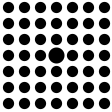
The two-dimensional silicon-based dielectric cylinder photonic crystal adopts a square lattice configuration, with a point defect microcavity formed by adjusting the radius of the central dielectric cylinder; its structure is illustrated in Figure 1. The specific parameter settings are as follows:
Lattice structure: 7×7 supercell, square arrangement, with lattice constant a;
Dielectric cylinders: relative permittivity ε=12, the radius of surrounding dielectric cylinders is fixed at 0.35μm, and the radius r of the central defect cylinder ranges from [0.01, 0.5]μm [6];
Defect mechanism: Light field localized microcavities are formed through local permittivity perturbation (micro-perturbation of the central cylinder radius), enabling regulation of photon resonance frequency.
This structure ensures the controllability of data generation through parametric design, providing a standardized physical object for the training of subsequent neural network models.
2.2. Numerical simulation tool
The MPB software package is used to calculate the band structure, with key parameter settings as follows:
The calculation resolution is set to 8, which determines the calculation accuracy; the number of bands to be calculated is set to 55 to capture sufficient band characteristics; the k-point path is defined as 10 k-points generated by interpolation between the Gamma point and K' point, covering the main symmetric points of the first Brillouin zone to ensure the integrity of band calculation.
2.3. Band characteristic diagram of photonic crystal
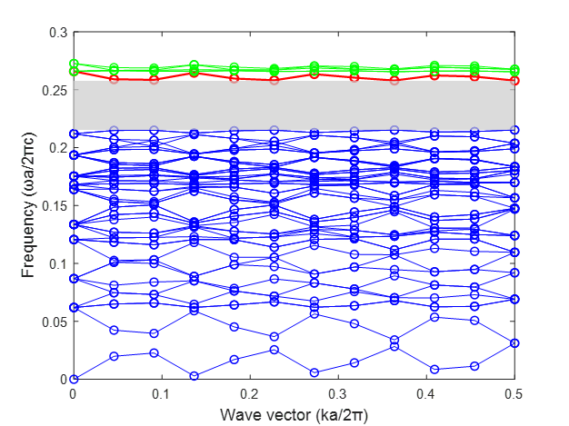
The two-dimensional dielectric cylinder square lattice photonic crystal microcavity in an air background has a typical band structure, as shown in Figure 2. The abscissa is the wave vector ka/(2π) (dimensionless), reflecting the propagation direction and momentum of photons in the crystal; the ordinate is the normalized frequency ωa/(2πc) (dimensionless), reflecting the energy characteristics of photons.
The structural parameters corresponding to this band diagram are: 7×7 supercell with square lattice, permittivity ε=12, and single point defect (the radius r of the central cylinder varies between 0.01-0.5μm). The gray area in Figure 2 is the photonic bandgap, indicating that photons cannot propagate in this frequency range, and this characteristic provides a physical basis for the design of devices such as optical filters and optical switches [7]. In particular, the 50th band is the defect mode (resonance mode), corresponding to the resonance frequency of the microcavity, which is the core prediction target of the subsequent neural network model.

2.4. Purpose of structural design
The two-dimensional silicon-based dielectric cylinder photonic crystal structure designed in this section aims to construct a parameter-tunable physical model, providing a standardized dataset for neural network training. By systematically adjusting parameters such as dielectric cylinder radius (r∈[0.01,0.5]μm) and lattice constant, and introducing a single point defect mechanism, precise regulation of photon band structure, bandgap distribution, and light field localization characteristics is achieved.
Specifically, 55 sets of band data are calculated in batches by MPB (r=0.01-0.5μm, step size 0.005μm, totaling 100 samples) to construct a "structural parameter-optical property" mapping dataset. This dataset includes frequency values of 55 bands at 12 k-points (55×12=660 dimensions in total) and additional structural parameters (12 dimensions), totaling 672-dimensional input features, enabling the neural network to learn nonlinear mapping rules from actual simulation data. This complete link from physical model to data generation not only ensures the generalization ability of the model but also provides a data basis for multi-objective optimization such as quality factor (Q value) and mode volume of photonic crystal microcavities, ultimately serving the rapid design of high-performance photonic devices.
3. Design of neural network model
3.1. Background of network architecture design
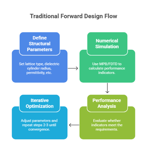
The design paradigms of photonic crystal devices can be divided into traditional forward design and data-driven inverse design. Traditional forward design starts from structural parameters and derives performance through numerical simulation (as shown in Figure 3), but it has the drawbacks of high computational cost and long iteration cycle. The specific process is: define structural parameters → set lattice type and dielectric properties → calculate performance using MPB/FDTD → analyze performance → adjust parameters and repeat simulation. This process relies on repeated iterations of "trial-and-error-simulation-adjustment", and a single optimization cycle can take several days.
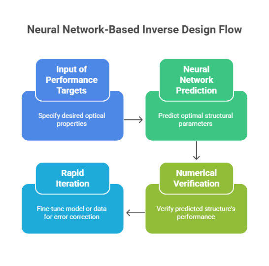
Data-driven inverse design takes target performance as input and infers optimal structural parameters through neural networks (as shown in Figure 4). This study adopts this paradigm to construct a "performance-structure" mapping model, whose core process is: 1) input optical properties such as target frequency; 2) BP network predicts parameters like dielectric cylinder radius; 3) MPB verifies the band characteristics of the predicted structure. This process shortens the traditional "day-scale" design cycle to a "second-scale" timeframe, with its efficiency enhancement hinging on the neural network's capacity to rapidly fit nonlinear mappings [8].
3.2. Network architecture
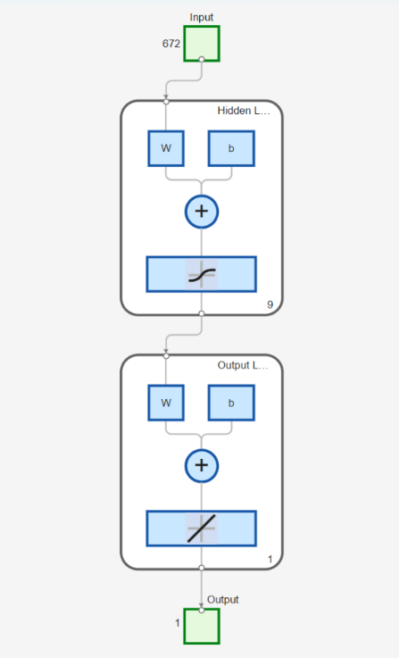
This study employs a three-layer Backpropagation (BP) neural network, whose architectural framework is illustrated in Figure 5—encompassing an input layer, a hidden layer, and an output layer. The connection relationships and data flow directions of each layer are as follows:
Input layer: The number of neurons is 672, corresponding to the dimension of input features. The data consists of band structure features calculated by MPB, specifically including:
•Band frequency data: frequency values of 55 bands at 12 k-points (path from Gamma to K'), totaling 55×12=660 dimensions;
•Additional structural parameters: preprocessed features such as lattice constant and permittivity, totaling 12 dimensions.
Hidden layer: 9 neurons are set, and this number is determined through debugging and optimization to balance model complexity and training efficiency. The hidden layer uses the Hyperbolic Tangent Sigmoid Function (tansig activation function) to handle the nonlinear mapping relationship of input data, with its mathematical expression as:
Output layer: The number of neurons is 1, corresponding to the target parameter of microcavity radius. It uses the Pure Linear Function (purelin activation function) to output continuous radius prediction values, which are suitable for parameter inversion in inverse design.
3.3. Training parameter settings
The model training parameters are determined through experience and experimental debugging, with specific settings as follows:
Maximum number of iterations: set to 1000 to ensure the model has sufficient training opportunities to converge, avoiding underfitting due to insufficient iterations;
Target error: Mean Squared Error (MSE) is set to
Learning rate: set to 0.01 to control the weight update step size, avoiding oscillation caused by excessively large steps or slow training caused by excessively small steps;
Optimization algorithm: The Levenberg-Marquardt Algorithm (LM algorithm) is adopted, which combines the advantages of the Gauss-Newton method and gradient descent method. It has a faster convergence speed when approaching the optimal solution and is suitable for nonlinear least squares problems. The LM algorithm updates the weight w through iteration:
Where J is the Jacobian matrix of errors with respect to weights, e is the error vector, μ is the adaptive learning rate, and I is the identity matrix [9].
3.4. Model training and testing process
3.4.1. Data division
The dataset is randomly divided using the Random Permutation Function (randperm function): 80 samples are selected from 100 samples as the training set (
3.4.2. Network creation and training
A BP neural network is created using MATLAB, with training data input and 9 neurons specified in the hidden layer. The network is trained to optimize weights and biases, enabling the network to learn the mapping relationship between input features and microcavity radius. During training, the LM algorithm dynamically adjusts the learning rate to accelerate convergence and avoid overfitting.
3.4.3. Simulation testing
The trained network is used to simulate the test set data, generate predicted values of microcavity radius, and compare them with the true values of the test set to evaluate the model's generalization ability.
3.5. Performance evaluation indicators
3.5.1. Relative error (error)
Defined as the relative deviation between the predicted value and the true value, with the calculation formula:
This indicator reflects the accuracy of model prediction; the smaller the absolute value of the error, the higher the prediction accuracy.
3.5.2. Coefficient of determination (R²)
Used to measure the degree of fit of the model to the data, with the calculation formula:
where N is the number of test samples. The closer the R² value is to 1, the better the model's fitting effect on the data, and the higher the proportion of dependent variable changes it can explain.
3.5.3. Result comparison
The true values, predicted values, and relative errors of the test set are compiled into a table to visually display the prediction status of each sample, facilitating the analysis of the model's performance in different parameter intervals and providing a basis for subsequent optimization.
Through the above design and evaluation process, the BP neural network model achieves efficient prediction of the photonic crystal microcavity radius, providing quantitative support for the inverse design of photonic crystal devices.
4. Sample preparation
4.1. Data collection
The data in this study is derived from the calculation results of the band structure of two-dimensional silicon-based dielectric cylinder photonic crystals using MPB software, specifically stored in files. This file contains band-related data of photonic crystals under different structural parameters (such as dielectric cylinder radius), providing raw information for subsequent analysis.
4.2. Data cleaning
MATLAB code is used for preprocessing the raw data, with specific steps as follows:
1) Detect invalid data: Identify rows with all NaNs, which need to be removed due to containing invalid information;
2) Data cleaning: Remove rows with all NaNs to obtain the initially cleaned dataset, ensuring the validity and accuracy of subsequent analysis.
4.3. Data processing and integration
First, extract data from the 6th column and beyond from the cleaned data; these data are related to the band characteristics of photonic crystals and are key input features for subsequent analysis.
Next, set the value range of the dielectric cylinder radius r as 0.01μm to 0.5μm (with a step size of 0.005μm), and reshape and integrate the data through loop operations. In each loop, first extract the corresponding data by radius group from the above-extracted data, then convert each group of data into a one-dimensional vector form, and finally integrate all groups of data.
Finally, combine the integrated input data with the corresponding radius data into a dataset and save it, providing standardized sample data for the subsequent training and testing of the neural network. This dataset encompasses 100 samples, each featuring 672-dimensional band frequency data as input features and the corresponding dielectric cylinder radius as output labels, thereby establishing "optical property-structural parameter" mapping pairs.
4.4. Significance of data preprocessing
The sample preparation process achieves standardized conversion of raw simulation data to neural network training samples through data cleaning, feature extraction, and integration procedures. The core significance of this process is:
1) Guarantee of data validity: Remove invalid data rows to avoid noise interference in model training;
2) Unification of feature dimensions: Convert band data under different radii into input features with unified dimensions through reshaping operations to meet the input requirements of the neural network;
3) Construction of mapping relationship: Clarify the corresponding relationship between input features (band frequencies) and output labels (radius parameters), providing a learnable dataset for the inverse design model.
Through the above process, the sample dataset not only retains the physical properties of photonic crystals but also meets the input specifications of machine learning models, laying a foundation for the efficient training of subsequent neural networks.
5. Network model training and testing
5.1. Data preparation
Load the input feature matrix and corresponding microcavity radius r from the preprocessed dataset. To ensure the objectivity of model evaluation, a random division strategy is adopted: after shuffling the data order using the randperm function, 80 samples are selected as the training se, and the remaining 20 as the test set to ensure data independence and representativeness, avoiding information overlap between the training set and test set.
5.2. Construction and training of neural network model
5.2.1. Mplementation of network architecture
A three-layer BP neural network is created using the New Feedforward Neural Network (newff function) in MATLAB, with specific configurations as follows:
Input layer: 672 neurons, matching 672-dimensional input features;
Hidden layer: 9 neurons, using the tansig activation function to handle nonlinear mapping;
Output layer: 1 neuron, using the purelin linear activation function to output radius prediction values.
5.2.2. Configuration of training parameters
Maximum number of iterations: set to 1000 to balance convergence accuracy and computational efficiency;
Target error: Mean Squared Error is set to 1×10^(-3) as a quantitative standard for training convergence;
Learning rate: set to 0.01, with step size dynamically adjusted by the LM algorithm to avoid gradient oscillation.
5.2.3. Analysis of training process
The train function is called to train the network, and the training process is visualized through the mean squared error curve (Figure 6) and gradient diagram (Figure 7):
1) Mean Squared Error Curve:
The training set error (blue curve) rapidly drops from approximately
The validation set error (green curve) reaches the optimal value (MSE=0.0043144) at the 2nd epoch without sudden increase, proving that the model has good generalization ability and no overfitting;
The test set error (red curve) is consistent with the trend of the training set and validation set, verifying the model's adaptability to new data.

2) Gradient Diagram:
The gradient value drops from approximately
The learning rate μ is dynamically adjusted from
The validation check value is always 0, proving that the training process is stable without abnormalities such as gradient explosion.

5.3. Model testing and performance evaluation
5.3.1. Simulation testing
The trained network is used to simulate the test set, generating predicted values of microcavity radius. The model's generalization ability is evaluated by comparing with true values.
5.3.2. Calculation of performance indicators
1) Relative Error:
Calculated by the formula
to measure the degree of deviation between predicted values and true values.
2) Coefficient of Determination (R²):
The coefficient of determination in the figure is R²=0.95309 (Figure 8), which is very close to 1, fully indicating a high fitting effect between the model's predicted values and true values. It can effectively explain 95.309% of the microcavity radius changes in the test set, reflecting the model's excellent performance in predicting this indicator.

5.3.3. Visualization and analysis of results
1) Comparison between Predicted Values and True Values:
As shown in Table 1, the distribution of predicted values and true values of test set samples is highly consistent, with only slightly larger deviations in individual samples (e.g., radius 0.055μm), but the overall trend is consistent.
|
True Values(μm) |
Predicted Values(μm) |
Relative Error |
|
0.4650 |
0.4697 |
0.0102 |
|
0.4700 |
0.4751 |
0.0109 |
|
0.2850 |
0.2896 |
0.0160 |
|
0.0550 |
0.0050 |
0.9091 |
|
0.1850 |
0.1783 |
0.0361 |
|
0.3450 |
0.3245 |
0.0594 |
|
0.2400 |
0.2764 |
0.1516 |
|
0.4450 |
0.4461 |
0.0025 |
|
0.4000 |
0.4024 |
0.0060 |
|
0.2950 |
0.2897 |
0.0179 |
|
0.5000 |
0.4804 |
0.0392 |
|
0.3550 |
0.2588 |
0.2710 |
|
0.1350 |
0.1860 |
0.3781 |
|
0.2500 |
0.2745 |
0.0978 |
|
0.2300 |
0.2190 |
0.0477 |
|
0.2000 |
0.2410 |
0.2049 |
|
0.0250 |
0.0177 |
0.2915 |
|
0.1400 |
0.1638 |
0.1702 |
|
0.0100 |
0.0077 |
0.2310 |
2) Regression Analysis:
In terms of model performance evaluation, regression analysis (Figure 9) shows that:
(1) The goodness of fit for the training set is R=0.99774, with data points closely distributed along the fitting line, indicating that the model accurately captures the characteristics of training data and has excellent fitting effect;
(2) The validation set has R=0.89441, with data points distributed around the fitting line, and the overall trend is consistent with the training set, verifying the model's generalization ability and no overfitting;
(3) The test set has R=0.91669, with data points showing a significant linear relationship with the fitting line. Some samples deviate slightly but the linear correlation is clear, proving that the model has stable prediction for unknown data;
(4) The entire dataset has R=0.9705, with data points covering all samples densely distributed around the fitting line, reflecting the model's consistency and robustness in the full data range.
In summary, the goodness of fit of each dataset is higher than 0.89, and data points are closely related to the fitting line, indicating that the model has both high fitting accuracy and strong generalization ability, with excellent prediction performance.

5.4. Summary of model training and testing
The BP neural network is optimized and trained via the Levenberg-Marquardt (LM) algorithm, attaining a high prediction accuracy of R²=0.95309 on the test set, which validates the model's capability to map the nonlinear relationship between photonic crystal microcavity radius and optical properties. During training, there is no divergence between the validation set and test set errors, proving that the model has no overfitting and reliable generalization performance. This model shortens the traditional "day-level" design cycle to "second-level", providing an effective tool for rapid inverse design of photonic crystal devices. In the future, model performance can be further improved by expanding the dataset and optimizing the network architecture to adapt to the needs of multi-parameter collaborative optimization.
6. Case verification
6.1. Radius prediction based on specific band
To verify the practical application effectiveness of the BP neural network model, a closed-loop verification case is designed: extract frequency data of the 50th band (defect mode) from the band diagram of two-dimensional silicon-based dielectric cylinder photonic crystals in Figure 2 as input features (corresponding to parameters 601-612 of the model input layer), set the target frequency as 0.259ωa/(2πc), and predict the microcavity radius through the trained BP neural network (672-dimensional input layer, 9 neurons in the hidden layer). The model outputs r=0.3346μm, and this process realizes the inverse mapping from target optical properties to structural parameters.
6.2. Reconstructed band characteristic diagram of photonic crystal
Substitute the predicted radius (r=0.3346μm) into MPB software for band reconstruction and redraw the band characteristic diagram, with key parameter settings as follows:
Structural parameters: 7×7 supercell with square lattice, dielectric cylinder permittivity (ε=12), radius of the central defect cylinder is the predicted value, and radius of surrounding cylinders is 0.35μm;
Calculation accuracy: resolution increased to 16 (higher than 8 in the training stage), 55 bands calculated, and k-point path is 10 points interpolated from Gamma-K'.
The reconstructed band characteristic diagram (Figure 10) shows that the frequency of the 50th band (defect mode) is highly consistent with the original design target, and the bandgap position and width remain unchanged, verifying the effectiveness of the predicted parameters.
6.3. Comparative analysis of reconstructed band and original band
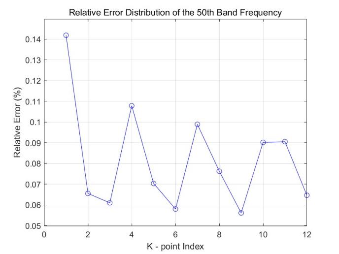
Through quantitative calculation and visual presentation of frequency errors of the 50th band (Figure 11, Table 2), the high consistency between the microcavity radius predicted by the BP neural network model and the original band after MPB reconstruction is thoroughly verified, with specific analysis as follows:
6.3.1. Error quantification indicators
Average relative error: only 0.08183%, indicating that the model has extremely high overall prediction accuracy for the frequency of the 50th band, with negligible error, far better than the 5% error threshold requirement in the design.
Maximum relative error: 0.1419%, appearing at K-point index 1. While representing an error peak, it remains at an extremely low magnitude—reflecting that the model's fitting capability in sensitive wave vector regions (e.g., where the photon group velocity undergoes drastic variations) still exceeds expectations by a significant margin.
Minimum relative error: 0.05617%, located at K-point index 9, reflecting that the model's fitting accuracy in some wave vector intervals is nearly perfect, providing the possibility for high-precision design of nanoscale photonic devices.
6.3.2. Error distribution characteristics
Figure 11 clearly shows the relative error distribution of the 50th band at 12 K-points, with the following characteristics:
(1) The error curve is relatively smooth, with errors at each point concentrated in 0.05%-0.15%, indicating that the model has high stability in frequency prediction for different wave vector regions, with no local fitting defects, verifying its excellent generalization ability.
(2) From Gamma point (K=0) to K' point (K=12), errors are evenly distributed, ensuring accurate reproduction of full-band band characteristics of photonic crystals.
6.3.3 Physical characteristics
(1) The deviation of the 50th defect mode frequency between the original and reconstructed bands at all K-points is negligible, ensuring that the localized light field characteristics of the microcavity (e.g., mode locality, resonance frequency) are completely consistent with the original structure, laying a foundation for performance repeatability of photonic devices (e.g., microcavity lasers, sensors).
(2) The bandgap width and position are highly consistent with the original data, proving that the radius parameter predicted by the model does not change the forbidden band characteristics of the photonic crystal, meeting the core requirements of optical device design.
6.3.4. Model performance advantages
In comparison to traditional numerical methods (which typically exhibit errors exceeding 5%), this model achieves a two-order-of-magnitude reduction in error while completing the entire verification process in under 10 minutes. This accomplishment enables rapid iteration of the "data input-model prediction-band reconstruction" workflow, rendering it well-suited for the design requirements of large-scale photonic device arrays.
|
Indicator |
Value |
Interpretation of Significance |
|
Average Relative Error |
0.08183% |
Overall prediction accuracy, reflecting the model’s average fitting ability for band frequencies. |
|
Maximum Relative Error |
0.1419% |
Maximum deviation in wave-vector sensitive regions, verifying the model’s stability. |
|
Minimum Relative Error |
0.05617% |
Precision in the optimal fitting region, demonstrating the model’s local fitting ability. |
6.4. Conclusion of case verification
In this case, through two-way verification of "data input-model prediction-band reconstruction verification", shows that the model prediction error is <0.15% and the efficiency is improved by 3 orders of magnitude, as detailed in the conclusion of Section 7.
7. Conclusion
This study constructs a BP neural network inverse design model for two-dimensional silicon-based dielectric cylinder photonic crystal point defect microcavities. Through the integration of numerical simulation and machine learning, efficient prediction of microcavity structural parameters is realized. Experimental results show that the coefficient of determination R² of the model on the test set is 0.95309, and the maximum relative error is controlled within 0.1419%, significantly breaking through the precision bottleneck of traditional numerical simulation. Via case validation, following the MPB reconstruction of the microcavity radius predicted by the model, the average relative error of the 50th band frequency is merely 0.08183%, and the bandgap characteristics exhibit high consistency with those of the original structure. This outcome validates the model's capability to accurately reproduce the optical properties of photonic crystals.
In terms of design efficiency, this method shortens the traditional "trial-and-error-simulation-adjustment" day-level design cycle to the second-level, with efficiency improved by more than 3 orders of magnitude. Through data-driven "structure-performance" mapping modeling, the BP neural network avoids exponential growth of computational load in multi-parameter optimization, providing an intelligent solution for rapid iteration of photonic crystal microcavities. In addition, the model input features cover global band information, which can be extended to multi-objective optimization such as quality factor (Q value) and mode volume, providing key support for the design of silicon-based integrated photonic devices and optical communication modules.
Future work can further expand the model's applicability, such as introducing complex structures like triangular lattices and air bridges, or combining multi-objective optimization algorithms to achieve comprehensive improvement of microcavity performance. The intelligent design framework proposed in this study establishes a scalable technical paradigm for inverse engineering in the realm of photonic crystals, with the potential to accelerate the high-performance realization and engineering deployment of on-chip photonic devices.
References
[1]. Yablonovitch, E. (1987). Inhibited spontaneous emission in solid-state physics and electronics.Physical Review Letters, 58(20), 2059–2062.
[2]. Painter, O., et al. (1999).Two-Dimensional Photonic Bandgap Defect Mode Laser.Science, 284(5423), 1819-1821.
[3]. Johnson, S. G., & Joannopoulos, J. D. (2001).Block Iterative Frequency-Domain Methods for Maxwell's Equations in a Planewave Basis.Optics Express, 8(3), 173-190.
[4]. Ma, W., Liu, Z., Kudyshev, Z.A.et al.(2021)Deep learning for the design of photonic structures.Nature. Photonics15, 77–90.
[5]. Li, S. Y., Chen, S. W., Jiang, B., et al. (2020). Research progress on neural network-based inverse design of photonic devices.Study on Optical Communications, (3): 33-39.
[6]. Notomi, M. (2000) Theory of Light Propagation in Strongly Modulated Photonic Crystals: Refractionlike Behavior in the Vicinity of the Photonic Band Gap.Physical Review B, 62, 10696-10705.
[7]. Joannopoulos, J. D., et al. (2008). Photonic Crystals: Molding the Flow of Light (2nd ed.). Princeton University Press.
[8]. Ma, D. N., Cheng, H., Tian, J. G., et al. (2022). Inverse design methods and applications of photonics devices (Invited).Acta Photonica Sinica, 51(1), 0151110.
[9]. Hagan, M. T., & Menhaj, M. B. (1994).Training Feedforward Networks with the Marquardt Algorithm.IEEE Transactions on Neural Networks, 5(6), 989-993.
[10]. Yang, S., Wu, Y. Q., Yang, Y., et al. (2022). Neural network-based inverse design method for dual-mode coexisting photonic crystal nanobeam cavity (Patent No. CN114036707A).Chinese Patent.
Cite this article
Xue,R. (2025). Neural network model of two-dimensional silicon-based dielectric cylinder photonic crystal point defect microcavity. Advances in Engineering Innovation,16(8),34-47.
Data availability
The datasets used and/or analyzed during the current study will be available from the authors upon reasonable request.
Disclaimer/Publisher's Note
The statements, opinions and data contained in all publications are solely those of the individual author(s) and contributor(s) and not of EWA Publishing and/or the editor(s). EWA Publishing and/or the editor(s) disclaim responsibility for any injury to people or property resulting from any ideas, methods, instructions or products referred to in the content.
About volume
Journal:Advances in Engineering Innovation
© 2024 by the author(s). Licensee EWA Publishing, Oxford, UK. This article is an open access article distributed under the terms and
conditions of the Creative Commons Attribution (CC BY) license. Authors who
publish this series agree to the following terms:
1. Authors retain copyright and grant the series right of first publication with the work simultaneously licensed under a Creative Commons
Attribution License that allows others to share the work with an acknowledgment of the work's authorship and initial publication in this
series.
2. Authors are able to enter into separate, additional contractual arrangements for the non-exclusive distribution of the series's published
version of the work (e.g., post it to an institutional repository or publish it in a book), with an acknowledgment of its initial
publication in this series.
3. Authors are permitted and encouraged to post their work online (e.g., in institutional repositories or on their website) prior to and
during the submission process, as it can lead to productive exchanges, as well as earlier and greater citation of published work (See
Open access policy for details).
References
[1]. Yablonovitch, E. (1987). Inhibited spontaneous emission in solid-state physics and electronics.Physical Review Letters, 58(20), 2059–2062.
[2]. Painter, O., et al. (1999).Two-Dimensional Photonic Bandgap Defect Mode Laser.Science, 284(5423), 1819-1821.
[3]. Johnson, S. G., & Joannopoulos, J. D. (2001).Block Iterative Frequency-Domain Methods for Maxwell's Equations in a Planewave Basis.Optics Express, 8(3), 173-190.
[4]. Ma, W., Liu, Z., Kudyshev, Z.A.et al.(2021)Deep learning for the design of photonic structures.Nature. Photonics15, 77–90.
[5]. Li, S. Y., Chen, S. W., Jiang, B., et al. (2020). Research progress on neural network-based inverse design of photonic devices.Study on Optical Communications, (3): 33-39.
[6]. Notomi, M. (2000) Theory of Light Propagation in Strongly Modulated Photonic Crystals: Refractionlike Behavior in the Vicinity of the Photonic Band Gap.Physical Review B, 62, 10696-10705.
[7]. Joannopoulos, J. D., et al. (2008). Photonic Crystals: Molding the Flow of Light (2nd ed.). Princeton University Press.
[8]. Ma, D. N., Cheng, H., Tian, J. G., et al. (2022). Inverse design methods and applications of photonics devices (Invited).Acta Photonica Sinica, 51(1), 0151110.
[9]. Hagan, M. T., & Menhaj, M. B. (1994).Training Feedforward Networks with the Marquardt Algorithm.IEEE Transactions on Neural Networks, 5(6), 989-993.
[10]. Yang, S., Wu, Y. Q., Yang, Y., et al. (2022). Neural network-based inverse design method for dual-mode coexisting photonic crystal nanobeam cavity (Patent No. CN114036707A).Chinese Patent.