


1. Introduction
Since graphene, the field of atomically thin materials has experienced explosive growth in optoelectronics, driven by its exceptional electronic properties and mechanical flexibility. Graphene exhibits ultrahigh carrier mobility—exceeding 1×105 cm2 V-1 s-1 at room temperature in clean, encapsulated samples—and remains among the most conductive materials known [1]. This high mobility facilitates rapid transport in photodetectors. However, the lack of a bandgap and low optical absorbance per monolayer (typically <10 %) limit graphene’s standalone utility in light detection. In contrast, transition metal dichalcogenide (TMD) monolayers such as MoS2 and WSe2 possess direct band gaps (in the range of ~1.2-2.0 eV), enabling strong photon absorption and high on/off ratios in photodiodes. These properties make them inherently more suitable for photovoltaic photodetection [2].
Emerging two-dimensional semiconductors further extend functionality. Materials like InSe and Bi2O2Se demonstrate fast intrinsic response times and high sensitivity even in the near infrared red (NIR). Bi2O2Se, for example, exhibits responsivity of ~65 A W-1 at 1200 nm and ultrafast response (~1 ps) at room temperature thanks to its narrow bandgap and relatively good crystallinity from chemical vapor deposition (CVD) synthesis [3,4]. Additionally, self-driven van der Waals heterostructures combining WSe2 and Bi2O2Se enable broadband operation with fast, bias-free response [5].
Despite these advances, several critical challenges remain unresolved. Firstly, per-layer optical absorption is intrinsically low (<10 %), necessitating complex stacking or metamaterial strategies to enhance responsivity. Secondly, achieving wafer-scale, high-quality growth with uniform thickness and crystallinity remains hard—device-to-device variability is a significant barrier to commercialization. Thirdly, implementing high responsivity, high detectivity, fast response, and low dark current in the same device often leads to performance trade-offs. Photoconductive designs with high gain are typically slower, whereas ultrafast photodiode architectures may compromise responsivity. Furthermore, polarization-sensitive detection and multifunctional device integration (e.g., combining imaging with communication capabilities) remain underexplored areas, representing significant research gaps to be addressed for next-generation technologies.
Key performance metrics for 2D photodetectors include responsivity (R, in A W-1), external quantum efficiency (EQE), specific detectivity (D*, in Jones), dark current (Id), and response time (τ). Responsivity relates to how effectively incident photons are converted to current. EQE represents the fraction of photons converted to charge carriers. Detectivity combines sensitivity with noise performance. Dark current contributes directly to noise and degrades detectivity. Response time determines the usable bandwidth of photodetectors.
Strategies to optimize these metrics span several approaches. The first approach is heterostructure integration. Creating built-in electric fields via vertical stacking (e.g., TMD/TMD, graphene/TMD) or lateral junctions to enhance carrier separation and broaden the spectral response into UV-infrared ranges. These designs exploit Type-II band alignment and built-in fields to simultaneously suppress dark current and boost responsivity [5]. The second approach is defect and doping engineering. Introducing controlled chalcogen vacancies, substitutional doping, or surface functionalization to tune carrier lifetime, doping levels, or built-in fields—strike a balance between gain, noise, and speed. The third approach is Interface passivation: Suppressing interfacial trap states via chemical treatments, encapsulation (e.g., h-BN layers), or surface oxides—to reduce dark current, suppress noise, and enhance stability. The last approach is device architecture design: Employing Schottky diodes, p-n junctions, photoconductors, and self-powered photodetector configurations to navigate the trade-offs between responsivity, speed, gain, and dark current.
This paper focuses on advances in scalability, device performance, and integration. Emphasis is placed on realistic pathways toward scalable, high-performance 2D photodetectors suitable for real-world applications. By synthesizing recent progress across materials optimization, heterostructure design, and architecture innovations, this review aims to identify performance bottlenecks and chart future directions. The analysis should guide materials scientists and device engineers toward creating next-generation 2D photodetectors that deliver flexible imaging, low-power optical communication, environmental sensing, and wearable detection capabilities.
2. Fundamental principles of two-dimensional materials in photodetectors
2.1. Theoretical foundations of the 2D photoelectric detector
The working principle of photodetectors based on two-dimensional materials mainly relies on the following three aspects: band theory, carrier dynamics, and light-material interaction.
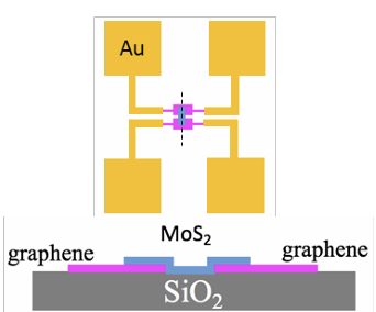
The band theory is a crucial foundation for understanding the response and performance of devices. This theory encompasses two main light detection mechanisms: the photovoltaic effect and photoconductive effect [6]. The photovoltaic effect occurs in structures with an intrinsic electric field, such as Schottky junctions or p-n heterojunctions [7,8]. When two-dimensional materials are exposed to light, photons can excite electron-hole pairs. These charge carriers are rapidly separated under the drive of the intrinsic electric field, with electrons being attracted to the n-type region and holes flowing to the p-type region, thereby generating current in the absence of bias. Such photovoltaic structures typically exhibit fast response and low dark current [9]. For example, in the 2D MoS2/p-Si heterostructure, due to the existence of the interface potential barrier, high-energy photons (such as visible or ultraviolet) can efficiently separate photogenerated electron-hole pairs and output photocurrent. The detection rate can reach 1013-1014 Jones, demonstrating the high-performance advantage of this mode [10]. The structure of the device is shown in Figure 1.
The photoconductive effect depends on the applied bias voltage, and the photoconductive device involves carrier dynamics, which determine the gain and speed of the device. Under bias voltage, the carriers are driven towards the electrode region, generating leakage current. Crucially, trap-mediated carrier localization, such as via defect states or interfacial traps, delays charge recombination, leading to a prolonged effective carrier lifetime (τ) [11]. Due to the average transport time (τt) of carriers being much shorter than the τ, the photogenerated carriers generated by each photon can participate in multiple cycles and be collected multiple times through the channel. The gain approximately satisfies the relationship G ≈ τ / τt, and the responsivity can reach 106 A/W [5,12]. Taking black phosphorus (BP) as an example, it is prone to form defects and has relatively low mobility channels. The device exhibits a remarkably strong photoelectric response exceeding 106 A/W in the NIR spectral region, while its temporal response is limited to the microsecond-to-millisecond range owing to the substantial τ [8].
The light-matter interaction in a two-dimensional system can be quantified by the EQE, which is defined as the ratio of the number of collected charge carriers to the number of incident photons [7]:
Among them, Iphrepresents the photocurrent, Popt (λ) is the optical power at wavelength λ, hv is the photon energy, and e is the electron charge. Despite the ultrathin nature (<1 nm), monolayer two-dimensional materials exhibit strong excitonic effects that enable external quantum efficiencies exceeding 40% in certain device architectures. After the material is combined with plasmas or optical resonators, the absorption capacity can be improved by more than ten times [7].
2.2. Typical spectral range of photodetectors
2.2.1. Ultraviolet-visible light (200-700 nm)
In the UV-visible wavelength range, photodetectors based on wide-bandgap two-dimensional materials, such as GaSe, Transition metal dichalcogenides (TMDs) and GaSe/MoS2 composite junctions, are more favored due to their strong layer-dependent absorption and clear band-edge characteristics. The single-layer or few-layer fragments of GaSe have a direct bandgap of approximately 2.0 eV, enabling efficient photon absorption near 350 nm. For example, the type II heterojunction device of GaSe/MoS2 achieves a response of ~42.6 A/W and a detection rate of ~8×10¹² Jones at a wavelength of 300 nm, with its performance being three times that of a single-layer MoS2 device [7]. Additionally, the simple-exfoliated GaSe device achieves a response of about 5 A/W under 405 nm laser irradiation of 42 mW/cm2, with extremely low dark current (~21 pA) and a slow response speed (rise time of about 34 ms), mainly influenced by the photoconductive mechanism. Such devices can be fabricated through vapor-phase growth or exfoliation, but large-scale, high-quality industrial production remains challenging. Furthermore, WSe2/graphene heterojunction has an EQE of over 50% under visible light [7,13].
2.2.2. Near infrared-short wave infrared (700-1700 nm)
The bandgap of the layer thickness of black phosphorus (BP) can be adjusted over the visible light range to approximately 4 µm, and the carrier mobility can exceed 103 cm2/V·s. When BP is combined with PbS or PbSe quantum dots on two-dimensional materials such as MoS₂ to form a type II heterojunction interface, a responsivity of over 102 A/W can be achieved in the 1.55 µm band, and the SWIR detection rate is approximately 1011 Jones. The BP/In2Se3 ferroelectric-controlled vdW heterojunction further shows tunable photo response and enhanced contrast due to built-in polarization fields, enabling gate-modulated responsivity in nearIR. BP devices can be fabricated through precise transfer or CVD growth, but they are prone to degradation in the air and require encapsulation treatment [7,8]..
2.2.3. Terahertz (30-3000 μm)
Graphene possesses a zero bandgap and high mobility, making it an ideal material for terahertz detection. Graphene FETs with integrated antenna structures (such as bow-tie or plasma slot structures) utilize the photovoltaic effect (PTE) to achieve a NEP < 10-12 W/Hz1/2, a response time < 3.3 ns, and a broadband (0.5 - 10 THz) detection capability. These room-temperature THz detectors have a dynamic range covering four orders of magnitude and are suitable for high-resolution spectroscopy, imaging, and communication. The manufacturing process relies on CVD-grown graphene combined with nano-scale antenna patterns, although it has the potential for large-area scalability, it requires high alignment accuracy [8,14].
2.3. Performance characteristics of photodetectors
Based on the above materials and structures, high-performance two-dimensional photodetectors possess the properties of wideband detection, high responsivity (R), specific detectivity (D*), and fast response speed (τ or bandwidth fc). These figures of merit are interdependent and governed by the underlying physics and device architectures.
Firstly, through heterostructure stacking or hybridization, a wide spectrum operation from UV to THz can be achieved, demonstrating multi-mode detection capabilities [7,8].
Secondly, responsivity (R) expresses how effectively incident light power is converted into photocurrent. Its fundamental relation is [15]:
Where λ is the wavelength, q is the electronic charge, h is Planck’s constant, c is the speed of light, Iph is the photocurrent, and Po is the amount of optical power incident on the detector. In practice, R values range widely: photodiode devices exceed 103 A/W, BP devices can reach 106 A/W, and graphene/organic systems achieve >5×10⁵ A/W in the UV-visible range [7,8].
Thirdly, in terms of specific detectivity (D*), it normalizes detectivity to device area and bandwidth, capturing noise-limited sensitivity. It is defined as [15]:
Where A is the sensing area, Δf is the bandwidth, NEP is the noiseequivalent power, and IN is the total current noise. Van der Wall (VDW) heterostructures and 2D/Si devices often exceed 1012 Jones, FePSe3/MoS2 reaches 1.5×10¹³, and MoS2/GaAs heterojunction can reach above 1014 Jones [16]. Finally, response speed (τ or fc) is governed by carrier transit time, RC time constant [17]:
Where R is the load resistance and C is the capacitance. Oxygen sulfide devices achieve picosecond levels, waveguide structures have a bandwidth of tens of GHz, while BP devices have a slower response time (in the millisecond range). In summary, material selection, heterostructure design, and device structure determine the trade-offs in performance, providing customized optimization solutions for imaging, optical communication, and sensing applications [6,8].
3. Comprehensive analysis and discussion on the performance of photodetectors
3.1. Performance analysis and challenges
A systematic comparison of optimization strategies for two-dimensional material photodetectors reveals that there are performance trade-offs among various methods. Van der Waals Type-II heterostructures, such as MoS2/WSe2 and InSe/graphene, utilize the built-in electric field to achieve efficient carrier separation, with their detectivity D exceeding 1013 Jones and the responsivity reaching 103-104 A/W [8]. However, due to the trap capture mechanism, the response time is typically in the microsecond to millisecond range. In contrast, plasma-enhanced devices concentrate the light field through metal nanostructures, enabling sub-nanosecond response while maintaining a responsivity of nearly 103 A/W. Nonetheless, the manufacturing process is complex and is limited by the effective area [18]. The fabrication process exhibits considerable complexity and is restricted by the effective area.
Ferroelectric-2D hybrid structures, such as ZnIn2S4/TMD, can achieve self-powered operation, with a D value of approximately 1012 Jones, a response rate of >103 A/W, and operation without bias [19]. Nevertheless, critical challenges remain in terms of cycle stability and material fatigue, which require further optimization. Hybrid dimensional structures, such as PbS QD/graphene, CNT/MoS2, provide broadband UV–SWIR detection and gains up to 105, yet uniformity and trap-limited response (about 100 µs) restrict their throughput in high-speed applications [20]. A comparative summary is shown in Table 1 below.
The common challenges faced by all platforms include dark current suppression, noise management, and spectral coverage issues. High-gain photovoltaic conductive devices typically exhibit elevated 1/f and generation‑recombination (g‑r) noise. Without strict noise equivalent power (NEP) characterization, D is prone to being overestimated [21]. To extend to mid-infrared, long-wave infrared, and terahertz frequency bands, additional hybrid or low-temperature operation is required, increasing system complexity and power consumption [22]. The large-scale and highly consistent fabrication of defect-free 2D layers and their heterojunctions remains a bottleneck for commercialization [6].
|
Strategy |
D (Jones) |
Responsivity (A/W) |
Speed (μs) |
Key Challenges |
|
Type-II Heterostructure [8,18,22] |
>1013 |
103-104 |
1-103 |
Trap-limited speed, synthesis scale |
|
Plasmonic Enhancement [18,23,24] |
~1014 |
~103 |
<10-3 |
Fabrication complexity, area coverage |
|
Ferroelectric Hybrid [19,25] |
~1012 |
>103 |
1-10-3 |
Fatigue, material stability |
|
Mixed-Dimensional [20] |
~1013 |
102-103 |
~100 |
Uniformity, noise |
3.2. Optimization methods for two-dimensional materials
3.2.1. Optimization via material structural engineering
Current performance optimization paradigms in materials engineering primarily involve the implementation of van der Waals heterostructures, organic hybrid architectures, two-dimensional/silicon heterojunctions, and defect passivation methodologies. Firstly, the vertically stacked structure with type-II band steps (such as MoS2/WSe2) can effectively separate charge carriers and broaden the spectral response to the ultraviolet-near infrared (UV-NIR) range [26]. Secondly, the organic-2D hybrid system combines the high mobility of graphene with organic semiconductors, leveraging their respective absorption and injection advantages to achieve a response rate greater than 103 A/W in the ultraviolet region [7]. Moreover, the 2D/silicon heterojunction can achieve a detection rate D > 1012 Jones at room temperature by combining mature silicon processes [6,8]. Finally, by chemically treating (such as super-acid treatment of MoS2) or hexagonal boron nitride encapsulation for defect passivation, the trap recombination can be reduced, and the NEP of dark current and noise can be decreased [6,7].
3.2.2. Optimization via device structure
In terms of device structure, by arranging metal nanostructures (such as Au nanowires/nanoparticles) near the two-dimensional layer to concentrate electromagnetic fields, a localized plasmon resonance can be formed with the two-dimensional layer. For example, periodic arrays of gold nano-disks or nanorods with diameters of approximately 18 nm, 60 nm, or 110 nm placed at controlled interparticle gaps (~2 nm) and surface-to-layer spacing produce intense nearfield “hotspots” at disk edges and between particles, tuned to ~530-630 nm resonance; these arrays yield photocurrent enhancements of over 800–1,500 % compared to bare material, while avoiding excessive parasitic capacitance. This can enhance absorption while maintaining response speed [8,14]. In waveguide integration, superimposing the two-dimensional layer onto a silicon waveguide enables a bandwidth greater than 50 GHz and a micron-scale size. Additionally, the thermoelectric or thermophotovoltaic effects of two-dimensional ferroelectric materials, such as ZnIn2S4, can be utilized to convert the temperature change, which is caused by light absorption, into an instantaneous electric potential. This method can achieve self-powered detection under zero bias, and has an inherent gain mechanism [6,8].
3.3. Application-oriented optimization
Imaging and sensing applications demand ultrahigh detectivity and minimal noise. MoS2/Si photodiodes, enhanced by surface passivation and resonant cavities, achieve D above 1013 Jones, enabling high-contrast, low-light imaging at room temperature [2]. Organic-2D hybrids further boost UV sensitivity, with responsivities nearing 1013 A/W under low-power illumination, facilitating flame detection and environmental monitoring [23].
In optical communications, speed is paramount. Ternary oxyselenide photodetectors (Bi2O2Se) deliver picosecond-scale response times (>100 GHz bandwidth) with moderate responsivity (~65 A/W), making them ideal for high-bit-rate interconnects [22]. Waveguide-integrated graphene devices also achieve >50 GHz operation within silicon photonics platforms, balancing CMOS compatibility with ultrafast performance [6].
Flexible and wearable electronics require mechanical robustness and low power. Printed CNT/graphene hybrid sensors maintain responsivity >102A/W under bending radii <5 mm, with self-powered architectures based on pyro-phototronic effects in ferroelectric 2D layers, ideal for health monitoring and e-skin applications [25]. However, their detectivity (~1010 Jones) and spectral range remain limited compared to rigid counterparts.
3.4. Performance optimization direction of photodetectors
To overcome scale and performance barriers, scalable synthesis of large-area, transfer-free 2D heterostructures via roll-to-roll CVD and direct growth on flexible substrates is under intense development. Advances in in situ passivation and layer-by-layer growth promise to reduce defects and maintain built-in field strengths across wafer scales [8].
Multifunctional integration—combining photodetection with memory, polarization sensitivity, and thermal sensing—has emerged as a promising research frontier. Ferroelectric-2D hybrids already demonstrate nonvolatile photogating, while anisotropic materials such as ReS2 and BP enable on-chip polarization-encoded imaging and encryption [27]. Quantum photodetectors leveraging single-photon avalanche in TMDC heterostructures and QD/2D hybrids aim to achieve single-photon sensitivity and timing resolution below 100 ps, critical for quantum communications and light detection and ranging (LIDAR) systems [24].
Progress in industrial-scale synthesis, multifunctional integration, and quantum-level sensitivity positions 2D-material photodetectors as critical enablers for next-generation optoelectronics, from ultrafast communications to quantum information processing.
4. Conclusion
This paper summarizes the methods for optimizing the performance of photodetectors based on two-dimensional nanomaterials and their mixed systems, and summarizes four main approaches: heterostructure engineering, defect and doping control, interface passivation, and innovative device architectures. Heterostructures, especially Type-II van der Waals stacking and hybrid-dimensional structures, achieve high detection rates by efficiently separating charge carriers and covering a wide spectral range; defect/doping engineering provides an effective means to regulate carrier lifetime and transmission performance, thereby achieving intentional trade-offs between responsivity and speed; interface passivation, such as encapsulation and chemical treatment, can significantly reduce trap states and dark current, directly improving noise performance and device stability; device structure innovation (plasma enhancement, waveguide integration, ferroelectric/thermoelectric hybridization, etc.) offers orthogonal approaches to enhance absorption, accelerate response, or achieve self-power supply. Overall, selectively combining these methods for specific target performance often approaches the ideal performance curve more closely than a single strategy.
These technological advancements have significant practical implications. The optimized two-dimensional photodetectors can offer advantages in terms of volume, weight, and flexibility that traditional bulk materials or III-V devices cannot match, thereby providing new solutions in areas such as wearable biosensing, foldable imaging arrays, portable environmental sensing, and on-chip optical interconnects. Moreover, two-dimensional materials can be precisely controlled at the atomic level to align the energy bands, reduce trap density, and modulate interface electric fields, enabling the detection function to be designed in coordination with electronic/optical components, thus achieving multi-functional integration such as sensing and storage, polarization selection, or on-chip spectral filtering. The development of low-power or self-powered systems also makes two-dimensional detectors suitable for energy-constrained scenarios such as the Internet of Things and distributed sensing.
To advance the laboratory progress to industrialization, future research should prioritize the following: First, achieve scalable and repeatable growth and integration processes to ensure the quality of grain boundaries and interfaces; second, establish standardized testing and reporting standards to make performance comparisons comparable and operational; third, promote the systematic integration of multi-functional devices, coupling detection, signal processing or memory functions onto a single chip; fourth, deeply explore quantum-level and polarization-sensitive detection mechanisms based on anisotropic or ferroelectric two-dimensional compounds. At the same time, long-term stability, packaging, and manufacturing costs are also key factors for technology implementation. Through collaborative efforts in material synthesis, device design, and system integration, two-dimensional photodetectors are expected to outperform existing solutions in several application scenarios and become the next generation of flexible, low-power, and wide-spectrum adaptable core components in optoelectronics.
References
[1]. Pezzini, S., Mišeikis, V., Pace, S., Rossella, F., Watanabe, K., Taniguchi, T. and Coletti, C. (2020) High-quality electrical transport using scalable CVD graphene. 2D Materials, 7(4), 041003.
[2]. Wei, Y., Lan, C., Zhou, S. and Li, C. (2023) Recent advances in photodetectors based on Two-Dimensional Material/SI heterojunctions. Applied Sciences, 13(19), 11037.
[3]. Gu, H., Zhang, T., Wang, Y., Zhou, T. and Chen, H. (2024) 2D Compounds with Heterolayered Architecture for Infrared Photodetectors. Chemical Science.
[4]. Li, T. and Peng, H. (2021) 2D BI2O2SE: An emerging material platform for the Next-Generation Electronic industry. Accounts of Materials Research, 2(9), 842–853.
[5]. Luo, P., Wang, F., Qu, J., Liu, K., Hu, X., Liu, K. and Zhai, T. (2020) Self‐Driven WSe2/Bi2O2Se Van der Waals Heterostructure Photodetectors with High Light On/Off Ratio and Fast Response. Advanced Functional Materials, 31(8).
[6]. Odebowale, A. A., Berhe, A. M., Somaweera, D., Wang, H., Lei, W., Miroshnichenko, A. E. and Hattori, H. T. (2025) Advances in 2D photodetectors: materials, mechanisms, and applications. Micromachines, 16(7), 776.
[7]. Malik, M., Iqbal, M. A., Choi, J. R., and Pham, P. V. (2022) 2D materials for efficient photodetection: overview, mechanisms, performance and UV-IR range applications. Frontiers in Chemistry, 10.
[8]. Nandihalli, N. (2024) Performance analysis of photodetectors based on 2D materials and heterostructures. Critical Reviews in Solid State and Materials Sciences/CRC Critical Reviews in Solid State and Materials Sciences, 49(6), 999–1085.
[9]. Dhyani, V. and Das, S. (2017) High-Speed scalable Silicon-MOS2 P-N heterojunction photodetectors. Scientific Reports, 7(1).
[10]. Han, P., St Marie, L., Wang, Q. X., Quirk, N., Fatimy, A. E., Ishigami, M. and Barbara, P. (2018) Highly sensitive MoS2photodetectors with graphene contacts. Nanotechnology, 29(20), 20LT01.
[11]. Kabatas, M. a. B., En-Nadir, R., Rahmani, K. and Eker, Y. R. (2023) Positive and negative photoconductivity in IR Nanofilm-Coated MOO3 Bias-Switching Photodetector. Micromachines, 14(10), 1860.
[12]. R. Paschotta, article on "Photoconductive Detectors" in the RP Photonics Encyclopedia, retrieved 2025-08-10.
[13]. Kumar, M., Park, J. and Seo, H. (2021) High-Performance and Self-Powered alternating current ultraviolet photodetector for digital communication. ACS Applied Materials & Interfaces, 13(10), 12241–12249.
[14]. Rao, G., Wang, X., Wang, Y., Wangyang, P., Yan, C., Chu, J., Xue, L., Gong, C., Huang, J., Xiong, J. and Li, Y. (2019) Two‐dimensional heterostructure promoted infrared photodetection devices. InfoMat, 1(3), 272–288.
[15]. Ji, C. H., Kim, K. T. and Oh, S. Y. (2018) High-detectivity perovskite-based photodetector using a Zr-doped TiOx cathode interlayer. RSC Advances, 8(15), 8302–8309.
[16]. Xu, Z., Lin, S., Li, X., Zhang, S., Wu, Z., Xu, W., Lu, Y., & Xu, S. (2016). Monolayer MoS 2 /GaAs heterostructure self-driven photodetector with extremely high detectivity. Nano Energy, 23, 89–96.
[17]. Jiang, J., Chen, H., Yang, F., Li, C., He, J., Wang, X. and Cui, J. (2025) The frequency response characteristics of Ge-on-SI photodetectors under high incident power. Nanomaterials, 15(5), 398.
[18]. Ahn, J., Yeon, E. and Hwang, D. K. (2025) Recent progress in 2D heterostructures for High‐Performance photodetectors and their applications. Advanced Optical Materials.
[19]. Huang, Q., Ma, C., Wang, N., Zhang, H., Lee, C. and Ma, Y. (2025) Photodetectors based on two-dimensional materials/ferroelectrics hybrid system: Physics, structures, and applications. Materials Science and Engineering R Reports, 164, 100986.
[20]. Liu, Y., Wang, F., Wang, X., Wang, X., Flahaut, E., Liu, X., Li, Y., Wang, X., Xu, Y., Shi, Y. and Zhang, R. (2015) Planar carbon nanotube–graphene hybrid films for high-performance broadband photodetectors. Nature Communications, 6(1).
[21]. Wang, F., Zhang, T., Xie, R., Wang, Z. and Hu, W. (2023) How to characterize figures of merit of two-dimensional photodetectors. Nature Communications, 14(1).
[22]. Yin, J., Tan, Z., Hong, H., Wu, J., Yuan, H., Liu, Y., Chen, C., Tan, C., Yao, F., Li, T., Chen, Y., Liu, Z., Liu, K. and Peng, H. (2018) Ultrafast and highly sensitive infrared photodetectors based on two-dimensional oxyselenide crystals. Nature Communications, 9(1).
[23]. Guo, L., Han, J. and Wang, J. (2023) Recent advances in enhancing the photodetector performance of 2D materials by combining them with organic thin films. Journal of Materials Chemistry C, 12(4), 1233–1267.
[24]. Li, X., Li, Z., Hu, J., Huang, B., Shi, J., Zhong, Z., Zhuang, Y., Chen, Y., Wang, J., Li, J., Zhang, L., Meng, X., Shi, W., Chen, S., Fang, X., Huang, H., Wang, J. and Chu, J. (2025) Tunneling-barrier-controlled sensitive deep ultraviolet photodetectors based on van der Waals heterostructures. Nature Communications, 16(1).
[25]. Du, C., Huang, Z., Zhou, J., Su, J., Yu, P., Zheng, Z., Yan, J., Yao, J., Chen, Y. and Duan, X. (2024) Self‐Trapped Excitons in 3R ZnIn2S4 with Broken Inversion Symmetry for High‐Performance Photodetection. Advanced Materials.
[26]. Wang, Y., Nie, Z. and Wang, F. (2020) Modulation of photocarrier relaxation dynamics in two-dimensional semiconductors. Light Science & Applications, 9(1).
[27]. Yu, L., Dong, H., Zhang, W., Zheng, Z., Liang, Y. and Yao, J. (2025) Development and challenges of polarization-sensitive photodetectors based on 2D materials. Nanoscale Horizons.
Cite this article
Li,S. (2025). Fundamental Characteristics of Photodetectors and Applications of Two-Dimensional Materials in Photodetection. Applied and Computational Engineering,181,72-81.
Data availability
The datasets used and/or analyzed during the current study will be available from the authors upon reasonable request.
Disclaimer/Publisher's Note
The statements, opinions and data contained in all publications are solely those of the individual author(s) and contributor(s) and not of EWA Publishing and/or the editor(s). EWA Publishing and/or the editor(s) disclaim responsibility for any injury to people or property resulting from any ideas, methods, instructions or products referred to in the content.
About volume
Volume title: Proceedings of CONF-FMCE 2025 Symposium: Semantic Communication for Media Compression and Transmission
© 2024 by the author(s). Licensee EWA Publishing, Oxford, UK. This article is an open access article distributed under the terms and
conditions of the Creative Commons Attribution (CC BY) license. Authors who
publish this series agree to the following terms:
1. Authors retain copyright and grant the series right of first publication with the work simultaneously licensed under a Creative Commons
Attribution License that allows others to share the work with an acknowledgment of the work's authorship and initial publication in this
series.
2. Authors are able to enter into separate, additional contractual arrangements for the non-exclusive distribution of the series's published
version of the work (e.g., post it to an institutional repository or publish it in a book), with an acknowledgment of its initial
publication in this series.
3. Authors are permitted and encouraged to post their work online (e.g., in institutional repositories or on their website) prior to and
during the submission process, as it can lead to productive exchanges, as well as earlier and greater citation of published work (See
Open access policy for details).
References
[1]. Pezzini, S., Mišeikis, V., Pace, S., Rossella, F., Watanabe, K., Taniguchi, T. and Coletti, C. (2020) High-quality electrical transport using scalable CVD graphene. 2D Materials, 7(4), 041003.
[2]. Wei, Y., Lan, C., Zhou, S. and Li, C. (2023) Recent advances in photodetectors based on Two-Dimensional Material/SI heterojunctions. Applied Sciences, 13(19), 11037.
[3]. Gu, H., Zhang, T., Wang, Y., Zhou, T. and Chen, H. (2024) 2D Compounds with Heterolayered Architecture for Infrared Photodetectors. Chemical Science.
[4]. Li, T. and Peng, H. (2021) 2D BI2O2SE: An emerging material platform for the Next-Generation Electronic industry. Accounts of Materials Research, 2(9), 842–853.
[5]. Luo, P., Wang, F., Qu, J., Liu, K., Hu, X., Liu, K. and Zhai, T. (2020) Self‐Driven WSe2/Bi2O2Se Van der Waals Heterostructure Photodetectors with High Light On/Off Ratio and Fast Response. Advanced Functional Materials, 31(8).
[6]. Odebowale, A. A., Berhe, A. M., Somaweera, D., Wang, H., Lei, W., Miroshnichenko, A. E. and Hattori, H. T. (2025) Advances in 2D photodetectors: materials, mechanisms, and applications. Micromachines, 16(7), 776.
[7]. Malik, M., Iqbal, M. A., Choi, J. R., and Pham, P. V. (2022) 2D materials for efficient photodetection: overview, mechanisms, performance and UV-IR range applications. Frontiers in Chemistry, 10.
[8]. Nandihalli, N. (2024) Performance analysis of photodetectors based on 2D materials and heterostructures. Critical Reviews in Solid State and Materials Sciences/CRC Critical Reviews in Solid State and Materials Sciences, 49(6), 999–1085.
[9]. Dhyani, V. and Das, S. (2017) High-Speed scalable Silicon-MOS2 P-N heterojunction photodetectors. Scientific Reports, 7(1).
[10]. Han, P., St Marie, L., Wang, Q. X., Quirk, N., Fatimy, A. E., Ishigami, M. and Barbara, P. (2018) Highly sensitive MoS2photodetectors with graphene contacts. Nanotechnology, 29(20), 20LT01.
[11]. Kabatas, M. a. B., En-Nadir, R., Rahmani, K. and Eker, Y. R. (2023) Positive and negative photoconductivity in IR Nanofilm-Coated MOO3 Bias-Switching Photodetector. Micromachines, 14(10), 1860.
[12]. R. Paschotta, article on "Photoconductive Detectors" in the RP Photonics Encyclopedia, retrieved 2025-08-10.
[13]. Kumar, M., Park, J. and Seo, H. (2021) High-Performance and Self-Powered alternating current ultraviolet photodetector for digital communication. ACS Applied Materials & Interfaces, 13(10), 12241–12249.
[14]. Rao, G., Wang, X., Wang, Y., Wangyang, P., Yan, C., Chu, J., Xue, L., Gong, C., Huang, J., Xiong, J. and Li, Y. (2019) Two‐dimensional heterostructure promoted infrared photodetection devices. InfoMat, 1(3), 272–288.
[15]. Ji, C. H., Kim, K. T. and Oh, S. Y. (2018) High-detectivity perovskite-based photodetector using a Zr-doped TiOx cathode interlayer. RSC Advances, 8(15), 8302–8309.
[16]. Xu, Z., Lin, S., Li, X., Zhang, S., Wu, Z., Xu, W., Lu, Y., & Xu, S. (2016). Monolayer MoS 2 /GaAs heterostructure self-driven photodetector with extremely high detectivity. Nano Energy, 23, 89–96.
[17]. Jiang, J., Chen, H., Yang, F., Li, C., He, J., Wang, X. and Cui, J. (2025) The frequency response characteristics of Ge-on-SI photodetectors under high incident power. Nanomaterials, 15(5), 398.
[18]. Ahn, J., Yeon, E. and Hwang, D. K. (2025) Recent progress in 2D heterostructures for High‐Performance photodetectors and their applications. Advanced Optical Materials.
[19]. Huang, Q., Ma, C., Wang, N., Zhang, H., Lee, C. and Ma, Y. (2025) Photodetectors based on two-dimensional materials/ferroelectrics hybrid system: Physics, structures, and applications. Materials Science and Engineering R Reports, 164, 100986.
[20]. Liu, Y., Wang, F., Wang, X., Wang, X., Flahaut, E., Liu, X., Li, Y., Wang, X., Xu, Y., Shi, Y. and Zhang, R. (2015) Planar carbon nanotube–graphene hybrid films for high-performance broadband photodetectors. Nature Communications, 6(1).
[21]. Wang, F., Zhang, T., Xie, R., Wang, Z. and Hu, W. (2023) How to characterize figures of merit of two-dimensional photodetectors. Nature Communications, 14(1).
[22]. Yin, J., Tan, Z., Hong, H., Wu, J., Yuan, H., Liu, Y., Chen, C., Tan, C., Yao, F., Li, T., Chen, Y., Liu, Z., Liu, K. and Peng, H. (2018) Ultrafast and highly sensitive infrared photodetectors based on two-dimensional oxyselenide crystals. Nature Communications, 9(1).
[23]. Guo, L., Han, J. and Wang, J. (2023) Recent advances in enhancing the photodetector performance of 2D materials by combining them with organic thin films. Journal of Materials Chemistry C, 12(4), 1233–1267.
[24]. Li, X., Li, Z., Hu, J., Huang, B., Shi, J., Zhong, Z., Zhuang, Y., Chen, Y., Wang, J., Li, J., Zhang, L., Meng, X., Shi, W., Chen, S., Fang, X., Huang, H., Wang, J. and Chu, J. (2025) Tunneling-barrier-controlled sensitive deep ultraviolet photodetectors based on van der Waals heterostructures. Nature Communications, 16(1).
[25]. Du, C., Huang, Z., Zhou, J., Su, J., Yu, P., Zheng, Z., Yan, J., Yao, J., Chen, Y. and Duan, X. (2024) Self‐Trapped Excitons in 3R ZnIn2S4 with Broken Inversion Symmetry for High‐Performance Photodetection. Advanced Materials.
[26]. Wang, Y., Nie, Z. and Wang, F. (2020) Modulation of photocarrier relaxation dynamics in two-dimensional semiconductors. Light Science & Applications, 9(1).
[27]. Yu, L., Dong, H., Zhang, W., Zheng, Z., Liang, Y. and Yao, J. (2025) Development and challenges of polarization-sensitive photodetectors based on 2D materials. Nanoscale Horizons.