


1. Introduction
There are many kinds of 2D materials have been developed so far. Interestingly, there are various ways for these 2D materials to form different heterostructures and Moiré patterns. Based on advanced theoretical approaches and experimental approaches, it is possible to manipulate and characterize these heterostructures and Moiré patterns. It has been found that some useful and interesting properties and phenomena can happen in the heterostructure and superlattice of the 2D materials. These optical, electrical, etc. properties can be applied in the synthesis of new materials and facilitate the physical properties and chemical properties of them in actual applications. Since graphene is the first kind of 2D materials found by people and much research has been done for graphene, it is important to begin with a general review for the graphene.
2. Methods for Graphene Production
The methods employed for graphene production vary depending on the intended application. In industrial settings, one approach involves harnessing the surface tension of specific solvents to achieve the exfoliation of graphene into individual monolayers, each comprising just a single atom’s thickness [1]. Alternatively, a technique involves initially oxidizing graphene, followed by the use of a solvent for exfoliation, and concluding with a centrifugation step [1].
On a broader scale, a commonly employed method is known as chemical vapor deposition (CVD). However, CVD encounters significant challenges due to its high production costs and issues related to product quality [1].
In laboratory settings, silicon carbide serves as a suitable substrate for the controlled mechanical exfoliation of graphene layers [1]. The mechanical exfoliation process itself is relatively straightforward and consists of the repetitive peeling of graphene layers using scotch tape [2]. It’s worth noting that the extracted graphene remains invisible when observed under an optical microscope until it is positioned atop a silicon wafer with a compatible thickness of SiO2 [2].
For a visual representation of this process, please refer to Figure 1, which illustrates the methodology used to render the extracted graphene visible, with the graphene layer positioned atop a silicon wafer featuring the appropriate SiO2 thickness [2].
|
Figure 1. Visualization of Extracted Graphene. |
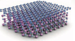
This figure provides an illustration of the technique used to make the extracted graphene visible. The graphene layer is placed atop a silicon wafer with SiO2 of suitable thickness, allowing for its observation and analysis [2].
3. Potential Future Applications of Graphene
Graphene has long been the subject of theoretical predictions, including the anticipation of two novel Quantum Hall Effects (QHEs)—namely, the quantum conductivity limit and resistance against quantum interference effects [2]. Building upon current research findings, this section delves into the promising applications that graphene could offer in the future.
Primarily, graphene’s exceptional attributes, encompassing flexibility, electrical conductivity, and chemical stability, position it as a potential replacement for Indium Tin Oxide (ITO) in screen displays [1]. Furthermore, experimental evidence underscores graphene’s capability to excel in the realm of high-frequency transistors [1]. Its impressive on/off ratios present a solution to the challenges confronting traditional logic resistors.
Graphene’s remarkable capacity to absorb incident light at normal angles renders it suitable for a multitude of photonic devices, including photodetectors, optical modulators, mode-locked lasers, and polarization controllers, among others [1].
Beyond these numerous applications, graphene’s potential extends to fields such as energy storage, sensors, metrology, and bio-applications, underscoring its profound promise for the future [1]. The multifaceted nature of graphene’s attributes ensures its relevance across a broad spectrum of scientific and industrial domains.
In sum, graphene’s potential applications are far-reaching, spanning from advanced electronics to photonics and even encompassing pivotal roles in energy solutions and bio-related endeavors. As research continues to unfold, the transformative possibilities of this exceptional material are poised to reshape numerous facets of technology and science.
4. The Unique Characteristics of Graphene
Graphene’s remarkable properties extend beyond the confines of strict two-dimensionality. In fact, due to its structural flexibility, graphene exhibits a versatile range of dimensionalities, including 0D buckyballs, 3D graphite, and 1D nanotubes [2]. The transformation between these dimensions is graphically represented in Figure 2.
|
Figure 2. Transition Between Graphene Dimensions. |
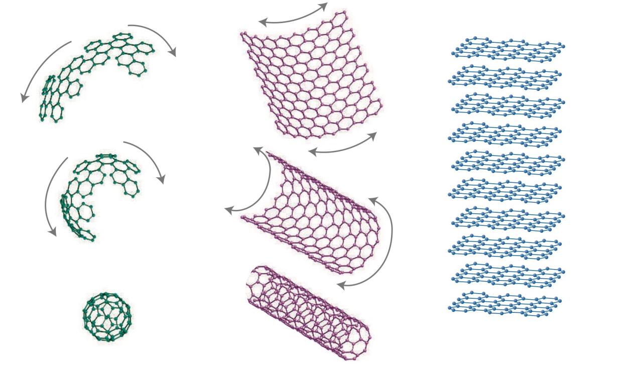
This figure visually illustrates the adaptability of graphene across different dimensionalities, encompassing 0D buckyballs, 3D graphite, and its native 2D form [2].
Graphene’s inherent flexibility opens the door to a multitude of potential applications, including health monitoring, movement detection, and the development of sensor-equipped smart human-machine interfaces [3]. Moreover, graphene’s unique capacity to form heterostructures with other 2D materials further expands its utility. However, before delving into graphene’s heterostructure capabilities, it is essential to acknowledge its lattice structure. Optical microscopy reveals that graphene possesses two distinct types of edges: the zigzag and armchair configurations [2]. These crystallographic features are pivotal in shaping the moiré patterns that emerge within heterostructures.
|
Figure 3. Graphene’s Zigzag and Armchair Edges. |
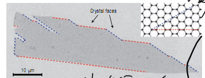
This figure distinguishes between the zigzag edge (represented by the blue line) and the armchair edge (represented by the red line) of graphene [2].
The specific crystal facets of graphene, as well as those of other 2D materials, play a crucial role in determining the intricate moiré patterns that characterize heterostructures. These patterns are instrumental in shaping the unique electronic properties of such composite materials. Understanding the interplay between lattice structures and heterostructures is fundamental to unlocking graphene’s full potential in future applications.
5. Heterostructures of Graphene and hBN with Moiré Patterns
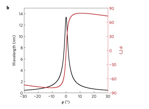
The concept of the “commensurate state” describes a scenario in which a crystal conforms to a periodic potential in a periodic manner [4]. Hexagonal boron nitride, often referred to as hBN, represents another intriguing 2D material capable of forming a heterostructure when stacked with graphene [4]. Research has revealed the occurrence of both commensurate and incommensurate transitions, contingent upon the relative angle between the two layers of 2D materials—a phenomenon previously theorized and now experimentally detected [4]. This distinction arises due to the formation of distinct moiré patterns within the heterostructure [4]. Figure 4 visually elucidates these moiré patterns, showcasing variations in moiré pattern periods. The moiré pattern period is determined by the relative rotational angle between the layers and can be expressed as:
\( λ=\frac{(1+δ)α}{\sqrt[]{{2(1+δ)(1-cos{ϕ})+δ^{2}}}} \) (1)
Where δ represents the lattice mismatch between hBN and graphene, a signifies the graphene lattice constant, and φ denotes the rotational angle between hBN and graphene [5].
Moreover, the relationship between the relative rotation angle and the graphene lattice is described as:
\( tan{θ}=\frac{sin{θ}}{(1+δ)-cos{ϕ}} \) (2)
With δ continuing to represent the lattice mismatch and φ signifying the graphene lattice [5]. These equations allow us to graph the moiré pattern period as a function of the relative rotation angle or the hBN lattice, as presented in Figure 5.
|
Figure 4. Different Moiré Patterns with Varying Angles. |
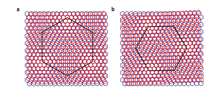
This figure illustrates diverse moiré patterns formed at different angles between the two layers, where ‘a’ represents the case with a 0° angle, and ‘b’ signifies an angle of approximately 0.052 radians. The red line represents graphene, and the blue line represents hBN [4].
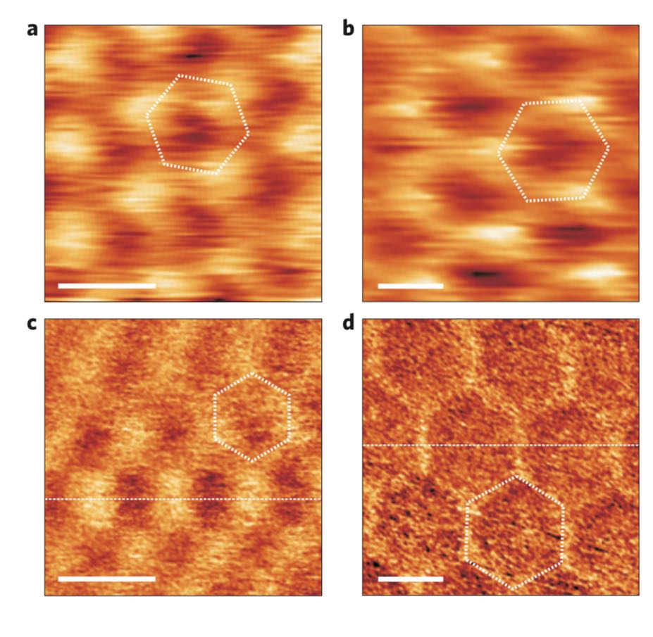
When the angles between the layers vary, the electronic spectrum of the heterostructure adjusts in tandem with the moiré potential, leading to alterations in the moiré pattern period [4]. Consequently, for smaller angles between the layers, the van der Waals interactions between them lead graphene toward a commensurate state, as the gained van der Waals energy compensates for the lost elastic energy [4]. Conversely, larger angles do not produce pronounced strain accumulation, resulting in an incommensurate state [4]. The real moiré patterns observed experimentally are depicted in Figure 6.
|
Figure 5. Moiré Patterns Observed in Experiments. |
Part ‘a’ illustrates measurements of 8nm moiré patterns using local resistance measured by conductive AFM. Part ‘b’ showcases 14nm moiré patterns. Parts ‘c’ and ‘d’ represent Young’s modulus distribution measured by PeakForce mode with 8nm and 14nm period moiré patterns, respectively [4].
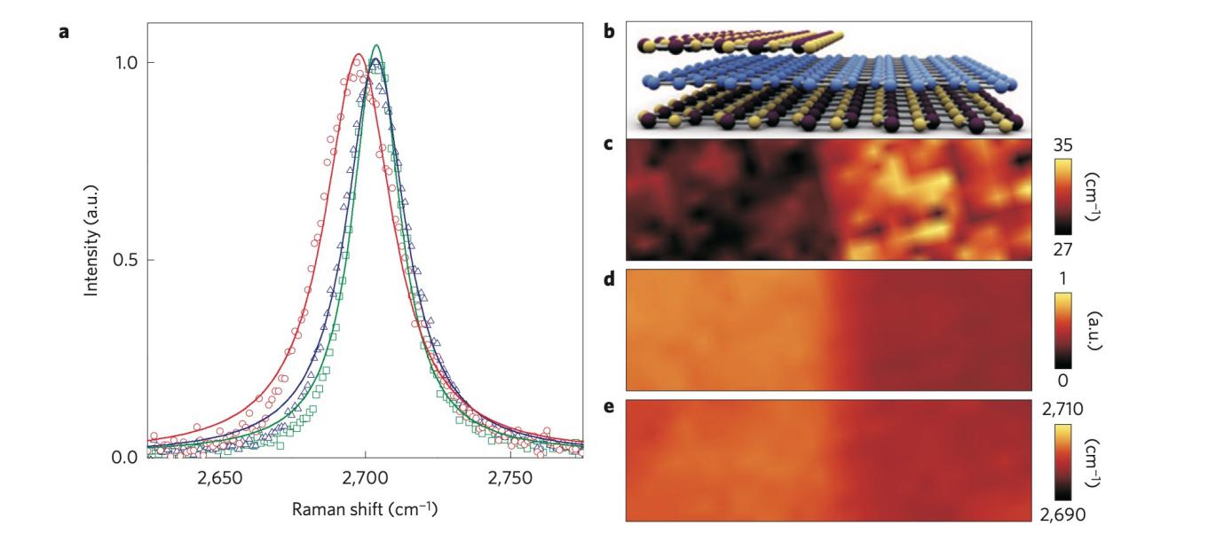
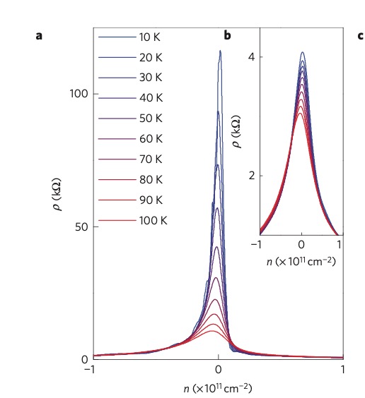
Various methods can be employed to detect moiré patterns. One approach involves Raman measurements, as depicted in Figure 7, where the presence of moiré patterns is indicated by the observed peaks in the graph [4]. Another method, known as transport measurement, is shown in Figure 8. Here, the peaks under different temperatures serve as evidence of the existence of moiré patterns [4].
|
Figure 6. Heterostructure of Graphene and hBN Measured by Raman. |
This figure displays samples of a graphene and hBN heterostructure subjected to Raman measurements [4].
|
Figure 7. Transport Measurements Reflecting Moiré Patterns. |
This figure presents data from transport measurements, showcasing the relationship between carrier concentration and longitudinal resistivity under different temperatures [4].
The interplay between moiré patterns and electronic properties within heterostructures reveals a rich landscape of possibilities. These patterns can be harnessed as a means of tailoring the behavior and properties of 2D materials, opening up exciting avenues for future research and applications.
|
Figure 8. The data from transport measurements, where the relationship between the carrier concentration and longitudinal resistivity is shown under different temperatures [4]. |
6. Preparation and Measurement of Super-Moiré Patterns
As previously discussed, the formation of a heterostructure with a moiré pattern, such as the combination of a single layer of graphene and a single layer of hBN, can give rise to additional Dirac points, thereby altering the electronic spectrum and various other material properties [6]. Building upon this insight, it has been discovered that by combining two moiré patterns, each formed by a single layer of hBN—one on top and one on the bottom—and a single layer of graphene in between, it is possible to generate super-moiré patterns [6]. This novel structure can potentially assume various low-energy states [6]. The process for creating these two moiré patterns and the subsequent formation of the super-moiré pattern, along with its verification, are illustrated in Figure 9. The preparation process bears similarities to the previous one, starting with the transfer of hBN onto silicon dioxide, followed by stacking hBN and subsequently placing graphene on top using polypropylene carbonate on Polydimethylsiloxane [6]. Initially, one layer of hBN is stacked, followed by graphene, and finally, the heterostructure is placed atop the prior hBN layer [6]. Subsequently, the AFM and Raman characterization techniques, employed previously, are utilized to detect both moiré patterns and the super-moiré patterns [6].
|
Figure 9. Super-Moiré Pattern Preparation and Verification. |
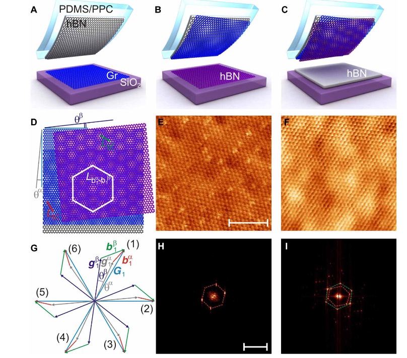
This figure illustrates the step-by-step procedures for creating two moiré patterns and the super-moiré patterns, as discussed earlier. Panel E depicts a single moiré pattern formed by one layer of hBN and one layer of graphene, captured using the AFM technique. Panel F, also using AFM, displays two moiré patterns formed by two layers of hBN and one layer of graphene. Panel G illustrates the lattice vectors resulting from different moiré patterns contributing to the lattice vector of the super-moiré pattern, with G1 representing the graphene lattice, gβ1 and g1α as the lattice vectors of the hBN layers, and b1α and b1β as the lattice vectors of the two moiré patterns [6].
Once the super-moiré pattern is identified, the transport properties of this three-layer heterostructure are measured, providing evidence of the existence of both moiré and super-moiré patterns (Figure 10).
|
Figure 10. Transport Property Measurements. |
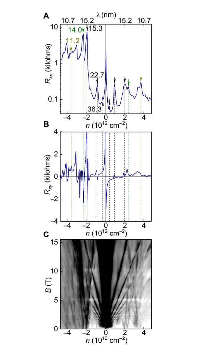
Panel A displays a graph depicting the relationship between longitudinal resistance and carrier concentration for the heterostructure, with arrows indicating peaks associated with the moiré patterns and super-moiré pattern. Panel B presents a similar measurement for the transversal resistance and carrier concentration, while Panel C depicts the relationship between Landau fans and carrier concentration [6].
As previously mentioned, the presence of moiré patterns or super-moiré patterns can also be inferred from peaks in the Raman spectrum. Utilizing this technique, various heterostructures discussed earlier were measured by Raman spectroscopy (Figure 11).
|
Figure 11. Raman Spectra for Different Heterostructures. |
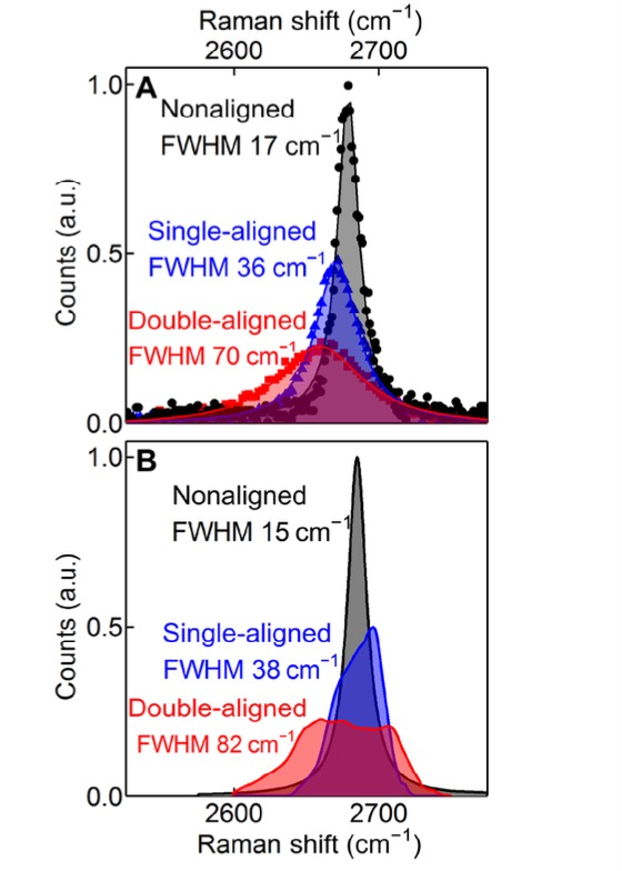
Panel A presents actual experimental results, with the sample without moiré patterns in gray, one moiré pattern in blue, and two moiré patterns in red. Panel B provides a corresponding simulation [6].
These advanced measurement techniques provide critical insights into the structural and electronic properties of super-moiré patterns, enabling a deeper understanding of their potential applications and effects on material behavior.
7. Superconductivity in Bilayer Graphene Superlattices
As previously discussed, superlattices composed of stacked layers of 2D materials exhibit a diverse array of properties, among which superconductivity has emerged as a particularly intriguing phenomenon. Remarkably, it has been observed that when two layers of graphene are stacked with a precise relative rotational angle, the electronic band structure undergoes a transformative shift, resulting in superconductivity at an unconventional temperature of 1.7K. This discovery ventures into the realm of strongly correlated materials and phenomena [7]. The theoretical underpinning of this phenomenon indicates that this optimal angle, often referred to as the “magic angle,” is theoretically predicted to occur at approximately 1.1°. At this angle, the energy bands become exceedingly flat, particularly in proximity to the zero Fermi energy [7]. Depending on the stacking order, the combination of energy bands can yield very low values [7], thereby reducing the Fermi velocity and altering the neutrality point of the charge [7]. Figure 12 illustrates the methodology for measuring superconductivity in these superlattices and showcases the manifestation of this extraordinary phenomenon.
|
Figure 12. Measuring Superconductivity in Graphene Superlattices. |
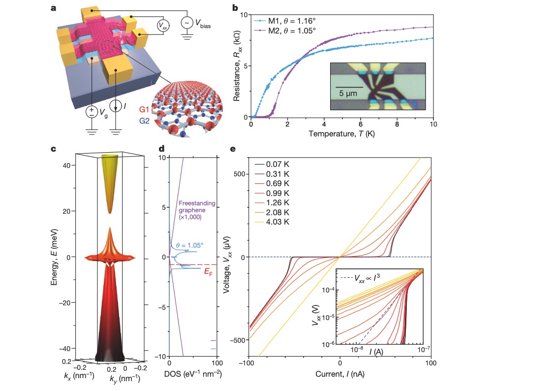
Panel ‘a’ presents an illustration of the device used for measuring superconductivity in the graphene heterostructure. It displays voltage readings (Vxx, Vbias, Vg) and current (I) connections between the two stacked layers of graphene (G1 and G2). Panel ‘b’ exhibits resistance measurements of the superlattice at two different relative rotational angles as a function of temperature. An optical image of the device is inset within panel ‘b’. Panel ‘c’ features a graph depicting the band energy of the superlattice with a relative rotational angle of approximately 1.05°, positioned within the first Brillouin zone. Panel ‘d’ illustrates the density of states (DOS) associated with panel ‘c’. Panel ‘e’ displays the relationship between voltage and current at various temperatures [7].
This groundbreaking discovery not only showcases the exceptional properties of bilayer graphene superlattices but also opens up new avenues for exploring unconventional superconductivity. Understanding the underlying physics and mechanisms of this phenomenon has the potential to revolutionize the field of materials science and condensed matter physics.
8. Superconductivity in Trilayer Graphene Superlattices
In a manner akin to the twisted bilayer graphene heterostructure, trilayer graphene subjected to significant rotational misalignment can yield moiré superlattices with what is often termed a “magic angle.” Strikingly, these trilayer graphene heterostructures exhibit superconductivity that is not only more pronounced but also more tunable in response to an electric field. This heightened tunability results in a broader phase diagram compared to bilayer heterostructures, bringing the system closer to the realm of Bose-Einstein condensates [8]. Evidence supporting superconductivity in such systems is marked by characteristics including zero-magnetic-field resistivity, substantial alterations in the voltage-current switching behavior, and Josephson phase coherence [8]. Notably, in trilayer graphene, flat bands reduce to bilayer graphene-like behavior, but the critical “magic angle” for trilayer graphene is larger, approximately 1.6° (Park 249). Figure 13 outlines the process for creating trilayer graphene moiré superlattices and characterizing their superconducting properties.
Panel ‘a’ illustrates the structure of trilayer graphene, with the bottom layer rotated at the negative “magic angle” and the top layer at the positive “magic angle” relative to the middle layer. Panels ‘b’ and ‘c’ present calculations of the band structure at 0 magnetic field. Panels ‘d’ and ‘e’ showcase data related to magneto transport, highlighting the presence of additional Landau levels. Panel ‘f’ features a graph representing longitudinal resistance and Hall conductivity as functions of 1/B. Panel ‘g’ depicts an estimation of the relationship between chemical potential and ν. Panel ‘j’ illustrates the relationship between voltage and current at varying temperatures. Inset images display resistance as a function of temperature and voltage as a function of current. The expanded range of zero resistance illustrates the enhanced tunability of the Trilayer Graphene Moiré Superlattice (MATTG) compared to bilayer superlattices [8].
This remarkable achievement in trilayer graphene superlattices not only underscores the exceptional properties of such structures but also extends the boundaries of our understanding of superconductivity. The potential applications and fundamental insights gained from these systems have the potential to significantly impact the fields of materials science and condensed matter physics.
|
|
|
|
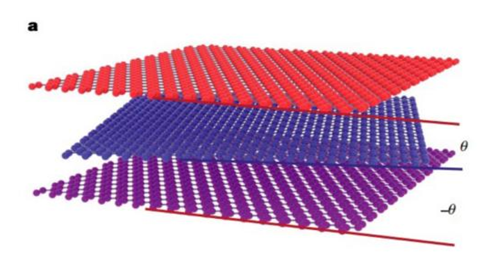
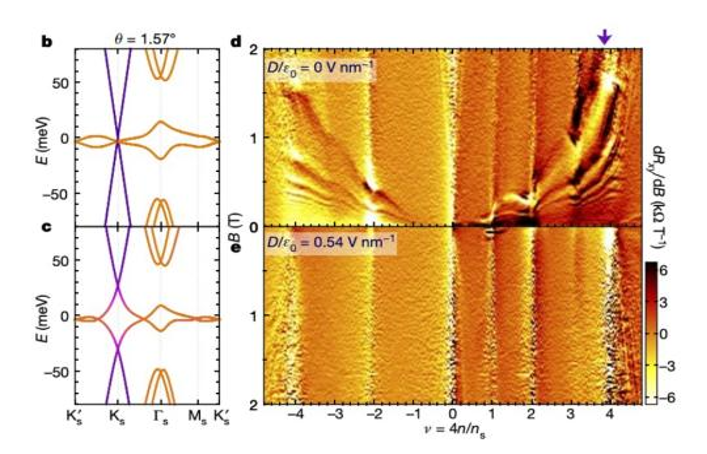
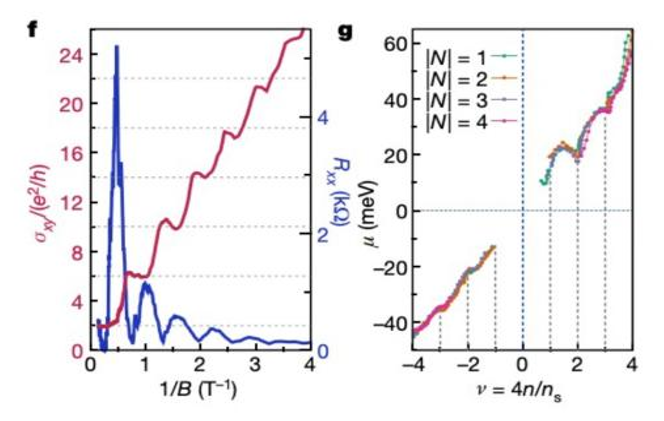
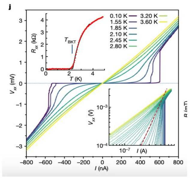
Figure 13. Trilayer Graphene Moiré Superlattice and Superconductivity Characterization.
9. Conclusion
In summary, this paper offers an extensive review of graphene, encompassing its historical development, unique properties, production methods, and potential applications. Moreover, it delves into the techniques for detecting and preparing moiré patterns or super-moiré patterns arising from graphene and hexagonal boron nitride (hBN) heterostructures. Most notably, it discusses the recent breakthrough in superconductivity observed within the superlattices of bilayer and trilayer graphene, accompanied by pertinent measurement methodologies.
This review provides a comprehensive overview of the progression of superlattice phenomena within 2D material heterostructures. In particular, it underscores the growing momentum toward harnessing graphene and other 2D materials for the development of devices exhibiting superconductivity, a field ripe for further exploration and research.
The evolution of graphene and the emergence of superlattice structures represent key milestones in the ongoing exploration of 2D materials, offering a wealth of possibilities for technological advancements and fundamental discoveries in condensed matter physics.
References
[1]. NOVOSELOV, K. S., et al. “A Roadmap for Graphene.” Nature (London), vol. 490, no. 7419, 2012, pp. 192-200.
[2]. Geim, A. K., and K. S. Novoselov. “The Rise of Graphene.” Nature Materials, vol. 6, no. 3, 2007, pp. 183-191.
[3]. Soe, H. M., et al. “Flexibility and Sensitivity of Graphene Nanoplatelets-Polydimethylsiloxane Strain Sensor.” AIP Conference Proceedings, vol. 2267, no. 1, 2020.
[4]. Woods, C. R., et al. “Commensurate-Incommensurate Transition in Graphene on Hexagonal Boron Nitride.” Nature Physics, vol. 10, no. 6, 2014, pp. 451-456.
[5]. Yankowitz, Matthew, et al. “Emergence of Superlattice Dirac Points in Graphene on Hexagonal Boron Nitride.” Nature Physics, vol. 8, no. 5, 2012, pp. 382-386.
[6]. Wang, Zihao, et al. “Composite Super-Moiré Lattices in Double-Aligned Graphene Heterostructures.” Science Advances, vol. 5, no. 12, 2019, pp. eaay8897-eaay8897.
[7]. Cao, Yuan, et al. “Unconventional Superconductivity in Magic-Angle Graphene Superlattices.” Nature (London), vol. 556, no. 7699, 2018, pp. 43-50.
[8]. Park, Jeong M., et al. “Tunable Strongly Coupled Superconductivity in Magic-Angle Twisted Trilayer Graphene.” Nature (London), vol. 590, no. 7845, 2021, pp. 249-255.
Cite this article
Li,L. (2024). A comprehensive review of superconductivity in heterostructures and superlattices comprising 2D materials. Applied and Computational Engineering,60,211-222.
Data availability
The datasets used and/or analyzed during the current study will be available from the authors upon reasonable request.
Disclaimer/Publisher's Note
The statements, opinions and data contained in all publications are solely those of the individual author(s) and contributor(s) and not of EWA Publishing and/or the editor(s). EWA Publishing and/or the editor(s) disclaim responsibility for any injury to people or property resulting from any ideas, methods, instructions or products referred to in the content.
About volume
Volume title: Proceedings of the 4th International Conference on Materials Chemistry and Environmental Engineering
© 2024 by the author(s). Licensee EWA Publishing, Oxford, UK. This article is an open access article distributed under the terms and
conditions of the Creative Commons Attribution (CC BY) license. Authors who
publish this series agree to the following terms:
1. Authors retain copyright and grant the series right of first publication with the work simultaneously licensed under a Creative Commons
Attribution License that allows others to share the work with an acknowledgment of the work's authorship and initial publication in this
series.
2. Authors are able to enter into separate, additional contractual arrangements for the non-exclusive distribution of the series's published
version of the work (e.g., post it to an institutional repository or publish it in a book), with an acknowledgment of its initial
publication in this series.
3. Authors are permitted and encouraged to post their work online (e.g., in institutional repositories or on their website) prior to and
during the submission process, as it can lead to productive exchanges, as well as earlier and greater citation of published work (See
Open access policy for details).
References
[1]. NOVOSELOV, K. S., et al. “A Roadmap for Graphene.” Nature (London), vol. 490, no. 7419, 2012, pp. 192-200.
[2]. Geim, A. K., and K. S. Novoselov. “The Rise of Graphene.” Nature Materials, vol. 6, no. 3, 2007, pp. 183-191.
[3]. Soe, H. M., et al. “Flexibility and Sensitivity of Graphene Nanoplatelets-Polydimethylsiloxane Strain Sensor.” AIP Conference Proceedings, vol. 2267, no. 1, 2020.
[4]. Woods, C. R., et al. “Commensurate-Incommensurate Transition in Graphene on Hexagonal Boron Nitride.” Nature Physics, vol. 10, no. 6, 2014, pp. 451-456.
[5]. Yankowitz, Matthew, et al. “Emergence of Superlattice Dirac Points in Graphene on Hexagonal Boron Nitride.” Nature Physics, vol. 8, no. 5, 2012, pp. 382-386.
[6]. Wang, Zihao, et al. “Composite Super-Moiré Lattices in Double-Aligned Graphene Heterostructures.” Science Advances, vol. 5, no. 12, 2019, pp. eaay8897-eaay8897.
[7]. Cao, Yuan, et al. “Unconventional Superconductivity in Magic-Angle Graphene Superlattices.” Nature (London), vol. 556, no. 7699, 2018, pp. 43-50.
[8]. Park, Jeong M., et al. “Tunable Strongly Coupled Superconductivity in Magic-Angle Twisted Trilayer Graphene.” Nature (London), vol. 590, no. 7845, 2021, pp. 249-255.