


1. Introduction
With the rapid advances in computer science, integrated circuits stand as the bedrock of technological progress, wielding pervasive influence across diverse domains [1]. Circuits such as absolute value detectors, play an indispensable role in driving modern advancements [2]. Conventional absolute value detectors commonly experience prolonged delays and elevated energy consumption [3]. Suppose the IC design can be optimized to reduce delay and power consumption. In that case, it can greatly improve the efficiency of large computer arrays such as supercomputers, enterprise servers, data centers, etc., and reduce heat generation, which is also in line with the concept of sustainable development [4]. This paper delves into the domain of integrated circuits, offering a 145.05 FO4 (0.82V), 7.23C Eu (0.82V) 4-bit absolute value comparator in CMOS logic.
This paper presents a 4-bit absolute value detector with a simplified adder circuit design aligned with functional requirements, significantly reducing the number of logic gates and diminishing circuit complexity. Strategic gate sizing and supply voltage adjustments play crucial roles in concurrently minimizing delay and energy consumption. This practical design strategy ensures a well-balanced and efficient operation of the comparator, highlighting its utility in signal processing applications. The study further scrutinizes the interplay between low energy consumption and minimal delay, employing a meticulous comparative analysis to fine-tune design parameters for optimal results. The delicate balance achieved between energy efficiency and responsiveness is a distinctive feature of this research effort.
This research not only improves the reliability of the device but also catalyses the acceleration of the signal response in real-world applications, optimizing the efficiency of the 4-bit absolute detector by simplifying the circuit design and energy-saving tuning, which contributes to the broader development of these fields [5]. The innovative design principles and strategic considerations outlined in this paper pave the way for advances in signal processing technology that promise to provide a more efficient and resilient foundation for future developments in electrical and electronic engineering and computer science and have the potential to promote the development of electrical and electronic engineering and computer science toward a faster, more robust, and more sustainable trajectory [6].
2. Design of the 4-bit Absolute Value Detector
2.1. Principle and Structure of the 4-bit Absolute Value Detector
In the context of digital signal processing, the 4-bit absolute value detector serves a critical role in discerning the magnitude of a signed input signal about a predetermined threshold value [7]. This specialized detector is meticulously designed in two distinct components to ensure efficiency and accuracy in its operation.
The first component, referred to as the Signed Value to Unsigned Value Transformer, plays a pivotal role in the conversion process. For the signed binary, the most significant bit is used to present the signs of this value [8]. The primary function of this transformer is to seamlessly transform the 4-bit signed input signal into an equivalent unsigned absolute value represented in 3 bits. This transformation is crucial in simplifying subsequent processing steps and ensures that the ensuing stages of the detector receive a standardized and consistently formatted input.
The second component of this sophisticated design encompasses a 3-bit Comparator, an integral element in the absolute value detection process. This comparator is responsible for meticulously comparing the input signal’s calculated absolute value, generated by the transformation stage, and the threshold value predetermined for the application. The outcome of this comparison is pivotal in determining whether the absolute value of the signed input signal surpasses the predefined threshold.
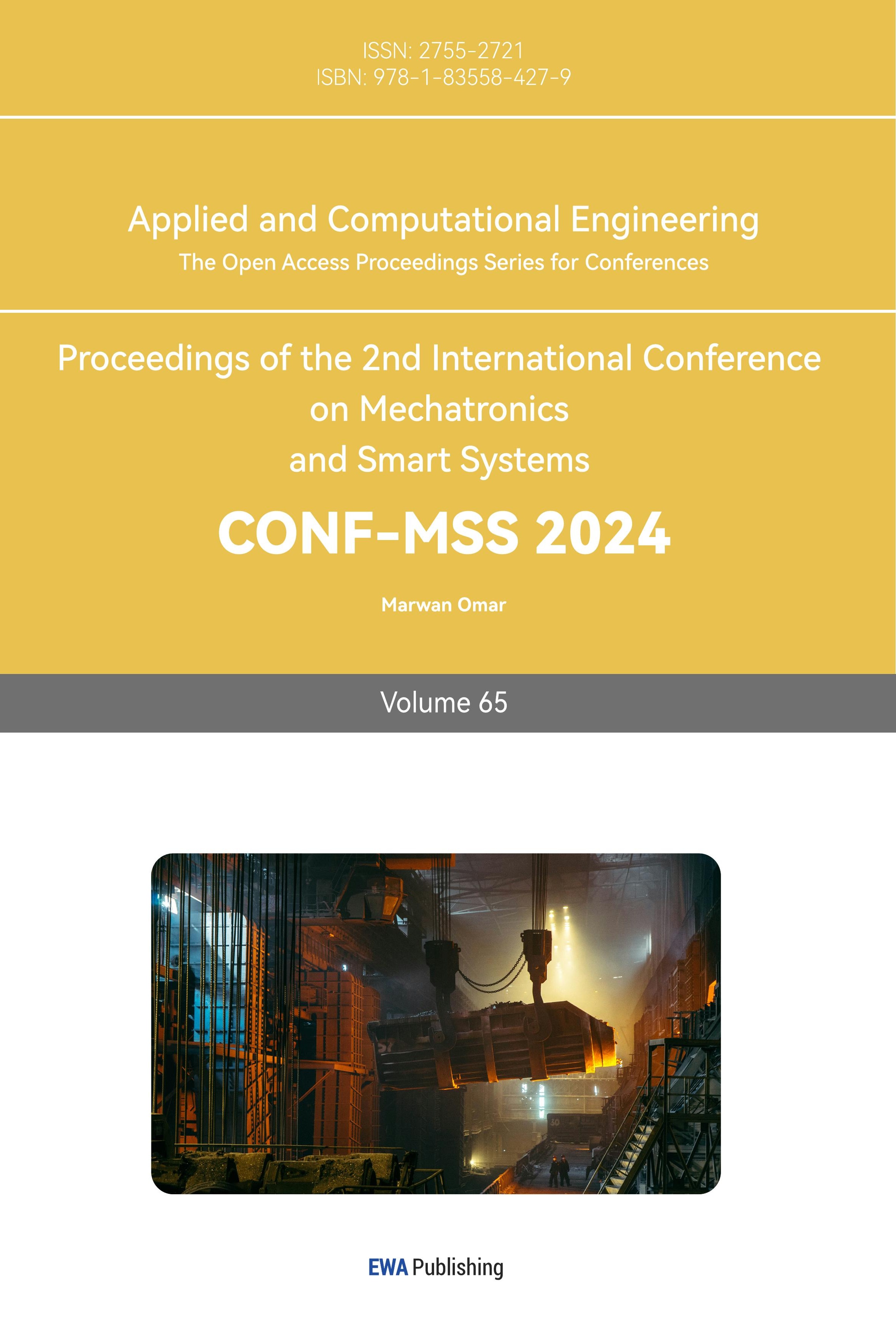
2.1.1. The Signed Value to Unsigned Value Transformer. To be more detailed, for the Signed Value to Unsigned Value Transformer shown in Figure 1, the transfer process has two cases: A3 equals 0 and A3 equals 1.
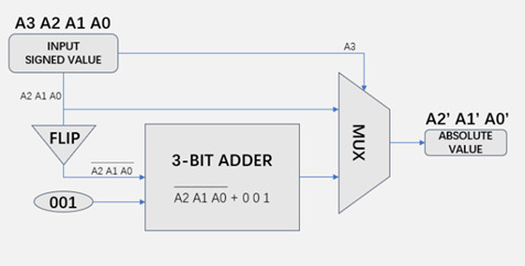
Figure 1. Structure of the Signed Value to Unsigned Value Transformer (Picture credit: Original)
Here, A3 is the sign of the 4-bit input. When A3 equals 0, it means that the 4-bit input is positive, therefore, A2 A1 A0 is the absolute value of the 4-bit input. While A3 equals 1, the input is negative, to obtain the absolute value, A2 A1 A0 will be flipped, and then add 001. As the absolute value is obtained, the value will be transmitted to the 3-bit comparator.
2.1.2. The 3-bit Comparator. For the 3-bit Comparator shown in Figure 2, first, a threshold value, B2 B1 B0 is set in advance, and the absolute value A2’ A1’ A0’ from the previous part compares with the threshold value from the less significant bit to the most significant bit (from A0’ to A2’).
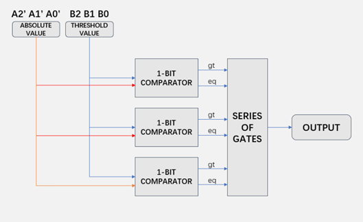
Figure 2. Structure of the 3-bit Comparator (Picture credit: Original)
For each stage of the bit-comparison, the 1-bit comparator will output two flags, eq, and gt (if A’ = B, eq = 1, else eq = 0; if A’ > B, gt = 1, else gt = 0). These flags are sent to a series of gates and then obtain an output.
2.2. Truth Table
A truth table is a tool used to describe the behavior of logic gate circuits [9]. Logic gate circuits are composed of logic gates that perform basic logic operations. A truth table lists the corresponding output values for each possible combination of inputs, providing useful information for designing and analyzing logic circuits. When constructing gate circuits, truth tables can help in the selection of logic gates. Second, the truth table helps in combinational logic circuit topology design, and by carefully studying the truth table you can determine how the logic gates are connected to realize the desired logic function. Most importantly, by looking at the truth table one can attempt to minimize logic expressions to simplify the circuit and reduce the number of components [9]. This is important in design because it reduces cost, power consumption, and complexity.
2.2.1. Truth Table for the 3-bit Adder. To build the Signed Value to Unsigned Value Transformer, the significant part is the 3-bit adder which plays the role of adding 001 to the inverter value of input. Normally, a 3-bit adder consists of three 1-bit adders, but in this case, one of the adders is fixed at 001. Therefore, the entire 3-bit adder can be viewed as a logic combination with 3-bit inputs and 3-bit outputs. As a result, the truth table can be obtained in Table 1.
Table 1. The truth table for the 3-bit Adder.
A0 | A1 | A2 | A0’ | A1’ | A2’ |
0 | 0 | 0 | 0 | 0 | 1 |
0 | 0 | 1 | 0 | 1 | 0 |
0 | 1 | 0 | 0 | 1 | 1 |
0 | 1 | 1 | 1 | 0 | 0 |
1 | 0 | 0 | 1 | 0 | 1 |
1 | 0 | 1 | 1 | 1 | 0 |
1 | 1 | 0 | 1 | 1 | 1 |
1 | 1 | 1 | 0 | 0 | 0 |
2.2.2. Truth Table of the 3-bit Comparator. The 3-bit comparator consists of three 1-bit magnitude comparator units and a series of logic gates link them together. One individual comparator unit has two inputs Ai’ and Bi, and it outputs two flags gti and eqi. Besides, here is a flag gtbi determines whether the Ai-1’ is greater than Bi-1, and these three flags gti, eqi, and gtbi together affect the next flag gtbi+1 and are transmitted to the next comparator unit. Therefore, the truth table for each 1-bit comparator unit is obtained in Table 2.
Table 2. Truth table for the 3-bit Comparator.
gtbi | eqi | gti | gtbi+1 |
1 | 1 | 0 | 1 |
1 | 0 | 1 | 1 |
1 | 0 | 0 | 0 |
0 | 1 | 0 | 0 |
0 | 0 | 1 | 1 |
0 | 0 | 0 | 0 |
2.3. The Circuit Design of the 4-bit Absolute Value Detector
Before constructing the circuit, it is necessary to determine the circuit style. Here the CMOS circuit style is chosen [10], where the ratio of channel width of n-type MOSFET to p-type MOSFET is Wn: Wp = 1.5. Therefore, it is possible to design various types of gate circuits such as NAND, NOR, XNOR, and multiplexers shown in Figure 3.
Figure 3. Circuit Style-CMOS (Picture credit: Original)
Based on the overall principle and structure as well as the truth table, a preliminary circuit topology diagram design for each part can be obtained. However, this is not the final circuit topology, which can be further optimized and streamlined after combining to get a lower overall energy consumption and lower delay.
2.3.1. Signed Value to Unsigned Value Transformer. According to the designed structure and the truth table, the circuit of the Singed Value to Unsigned Value Transformer is obtained, shown in Figure 4.
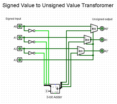
Figure 4. Circuit of Singed Value to Unsigned Value Transformer (Picture credit: Original)
2.3.2. 3-bit Adder. According to the designed structure and the truth table, the circuit diagram of a simplified 3-bit Adder that retains the required functionality can be obtained, shown in Figure 5.
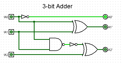
Figure 5. Circuit topology diagram of 3-bit Adder (Picture credit: Original)
2.3.3. 3-bit Comparator. According to the designed structure and the truth table, the circuit diagram of the 3-bit Comparator is obtained, shown in Figure 6.
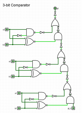
Figure 6. Circuit topology diagram of 3-bit Comparator (Picture credit: Original)
2.3.4. The Optimized Overall Cricuit of the 4-bit Absolute Value Detector. According to the above, the overall circuit is obtained, and by analyzing the circuit, some of the gates and multiplexers can be discarded. Finally, the optimized overall circuit of the 4-bit Absolute Value Detector is obtained, shown in Figure 7.
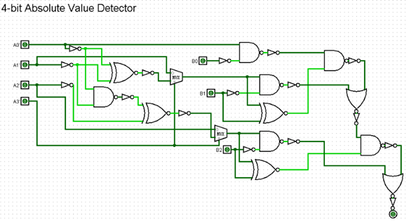
Figure 7. Overall circuit topology diagram of 4-bit Comparator (Picture credit: Original)
The integration of all components in the 4-bit absolute value detector results in a carefully optimized circuit topology, where certain gates and multiplexers can be strategically omitted to make the overall complexity of the circuit streamlined, leading to a more energy-efficient and faster implementation. This reduction in components not only minimizes power consumption but also mitigates propagation delays, contributing to an overall improvement in the detector’s performance. This optimized design not only enhances the detector’s performance but also aligns with contemporary considerations for energy-efficient and high-speed digital signal processing applications.
3. Calculation of the Performance of the 4-bit Absolute Value Detector
3.1. Basic Parameters
Before the comprehensive computation, it is imperative to derive certain fundamental parameters. The parameters to be ascertained in this context encompass Logical Effort (denoted as “g”) and Parasitic Effort (referred to as “p”).
Logical Effort is delineated as the quotient of the input capacitance to the input capacitance of an inverter yielding an equivalent output current. On the other hand, Parasitic Effort is characterized as the ratio between the intrinsic capacitance at the output and the intrinsic capacitance at the output of a corresponding inverter [11].
According to Figure 3, it is stipulated that for the Inverter configuration, the logical effort (g) is assigned a value of 1, and likewise, the parasitic effort (p) is also assigned a value of 1. Consequently, these designated values for g and p serve as benchmarks for determining the corresponding logical and parasitic efforts of the other logic gates and the multiplexer within the circuit. The value of g and p is shown in Table 3.
Table 3. The value of p and g
g | p | |
INV | 1 | 1 |
NAND | 1.4 | 2 |
NOR | 1.6 | 2 |
XNOR | 4 | 4 |
MUX | 8/3 | 4 |
3.2. Critical Path Analysis
The critical path, shown in Figure 8, identified as the route characterized by the maximum delay, holds paramount significance in circuit analysis.
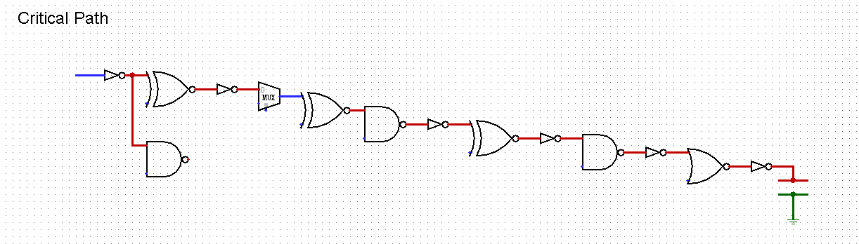
Figure 8. The critical path of the overall circuit (Picture credit: Original)
The initial step in pinpointing the critical path typically involves the identification of the longest path containing the highest number of gates. In instances where multiple paths exhibit an equivalent number of gates, the subsequent step entails a comparative assessment of gate complexities along each path. The path distinguished by the highest complexity is deemed the critical path [12].
Notably, within the devised topological structure, it is discernible that negative values traverse extended paths. Focusing specifically on the absolute-value extraction circuit and comparator, the critical path is ascertainable. It is imperative to underscore that all subsequent calculations, encompassing delay and energy consumption, occur post-buffer and pre-load. Consequently, the designated critical path pertains solely to the segment extending from the buffer to the load.
Before the analysis, It should be noted that the threshold value B is set to 011. This detector is driven by 2 unit-inverters and the output bit is loaded with 32 times the input unit inverter.
3.3. The Minimum Delay
The equation of delay is given [11] that:
\( Delay = \underset{ }{\frac{{V_{dd}}}{{({V_{dd}}-{V_{th}})^{2}}}·∑}({g_{i}}·{h_{i}}·{b_{i}}+{p_{i}}) \) (1)
In this design, the threshold value Vth is set to 0.2V, and the supply voltage range is 0~1V, to get the minimum delay, Vdd is set to 1V.
The following equation determines the total path effort of the critical path [11].
\( Path Logical Effort: {G_{path}} = {g_{1}}·{g_{2}}...{g_{N}} \) (2)
\( Branching Effort: {B_{path}} = {b_{1}}·{b_{2}}...{b_{N}} \) (3)
\( Path Electrical Effort: {H_{path}} =\frac{{C_{in}}}{{C_{out}}} \) (4)
\( Path Effort: {F_{path}} = {G_{path}}·{B_{path}}·{H_{path}} \) (5)
To make the delay minimum, each stage bears the same size, then the stage delay is also the same.
\( Stage Delay: f= \sqrt[N]{Path Effort} \) (6)
Therefore, the minimum delay can be presented as the following equation.
\( Dela{y_{min}} = \underset{ }{\frac{{V_{dd}}}{{({V_{dd}}-{V_{th}})^{2}}}·}(N·f+\sum _{ } {p_{i}}) \) (7)
According to the above equation, the minimum delay of the critical path can be obtained as 95.83. However, the overall circuit energy consumption is not considered, and to get a better energy efficiency for this design, the value of supply voltage needs to be adjusted and the circuit needs to be gate sizing.
3.4. Optimization
The following equation shows the relation of transition probability, gate sizing, and supply voltage [11].
\( E = {{V_{dd}}^{2}}·\sum _{ }{α_{i}}·{C_{i}} \) (8)
Table 4 chart shows the transition probability for each stage. At minimal delay, the size is all the same for every stage. Therefore, the energy consumption in this case is 15.43 unit-inverter.
Table 4. The transition probability α for each stage.
α1 | α2 | α3 | α4 | α5 | α6 | α7 |
1/4 | 1/4 | 1/4 | 1/4 | 1/4 | 3/16 | 3/16 |
α8 | α9 | α10 | α11 | α12 | α13 | |
3/16 | 3/16 | 15/64 | 15/64 | 15/64 | 15/64 |
To achieve better energy efficiency, the next step will be to calculate what supply voltage and how to gate sizing to get a “Balance Point” that has the minimum energy consumption with a delay near 1.5 times the minimum delay.
3.4.1. Adjusting Supply Voltage Only. Finding the “Balance Point” directly is complicated because there are multiple variables. Therefore, starting with one variable and getting its approximate range will simplify the subsequent research. Making the supply voltage Vdd vary between 0.7 and 1V, the plots of delay with Vdd and energy with Vdd can be obtained according to Equation 8. In Figure 9, the line charts show that when the gate size is the case in which delay is minimum, only if Vdd varies in the interval 0.77V to 1V can the delay reach 1.5 times the minimum delay. Also, it can be found that the energy consumption in this case is around 9.21 unit-inverter.
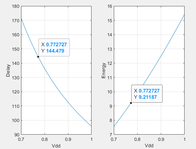
Figure 9. Vdd vs Delay and Vdd vs Energy (Picture credit: Original)
Therefore, by adjusting the supply voltage only, energy consumption has decreased by 40.31%, but the cost is a 50.77% increase in delay.
3.4.2. Adjust the Gate Size and Vdd. As the variation range of Vdd is found, by using Excel, the energy consumption and the delay can be calculated.
From the chart, it can be obtained that when the supply voltage Vdd is 0.83V, with the gate sizing shown in Table 5, the circuit has a minimum energy consumption of Emin = 7.23 unit-inverter.
Table 5. Gate sizing
1 | 2 | 3 | 4 | 5 | 6 | 7 |
0.25 | 0.35 | 0.05 | 0.05 | 0.05 | 0.05 | 0.10 |
8 | 9 | 10 | 11 | 12 | 13 | |
0.20 | 0.20 | 0.30 | 0.65 | 1.45 | 3.05 |
Here, by adjusting the supply voltage and gate size, energy consumption was reduced by 53.12% while increasing delay by 51.37%. Compared with adjusting supply voltage only, the energy consumption has dropped by 21.46%.
In Figure 10, this line chart shows the delay and energy consumption in different cases.
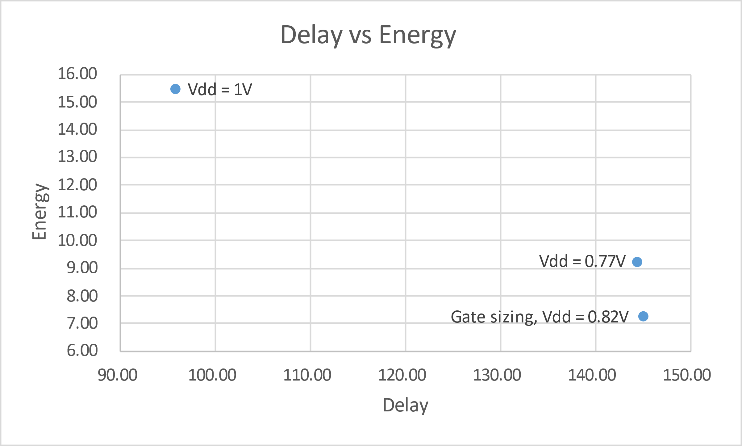
Figure 10. Delay vs Energy (Picture credit: Original)
4. Conclusion
In conclusion, this research marks a significant stride in optimizing integrated circuit (IC) design, presenting a 145.05 FO4 (0.82V), 7.23C Eu (0.82V) 4-bit absolute value detector with streamlined circuitry for enhanced reliability and accelerated signal response. The strategic integration of gate sizing and voltage adjustments not only minimizes delay and energy consumption but also promises broader applications in large computer arrays, aligning with the ethos of sustainable development.
Looking forward, the innovative principles introduced in this essay pave the way for advancements in signal processing technologies. Future perspectives include the potential for widespread adoption of these design strategies, contributing to a more efficient and resilient foundation for the evolution of electrical, electronic engineering, and computer science. This trajectory holds promise for faster, more robust, and sustainable developments in the field.
However, there are still areas where this design can be improved. First, if PTL is used instead of COMS inside some devices, such as multiplexers, this can lead to better performance parameters and thus better energy efficiency. Secondly, in terms of the balance between delay and energy consumption, using Excel to find a good gate size is inefficient and reduces the accuracy of the data obtained. In future research, better circuit architecture design is desired.
References
[1]. Iranmanesh S, Raikos G, Jiang Z, et al. CMOS implementation of a low power absolute value comparator circuit. 2016 14th IEEE International New Circuits and Systems Conference (NEWCAS). IEEE, 2016: 1-4.
[2]. Altuve M, Monroy N F. Hidden Markov model-based heartbeat detector using electrocardiogram and arterial pressure signals. Biomedical Engineering Letters, 2021, 11(3): 249-261.
[3]. Hirata M, Nagashima S, Cho T, et al. A Novel Electrostatic Ion-Current Absolute-Value Detector Under Circumstances with Simultaneous Electron Incidence by The Use of a Proposed “Self-Collection” Method for Secondary Electron Emission. Fusion science and technology, 2003, 43(1T): 262-264.
[4]. Nada S A, Elfeky K E, Attia A M A, et al. Experimental parametric study of servers cooling management in data centers buildings. Heat and Mass Transfer, 2017, 53: 2083-2097.
[5]. Huang Z. Performance Optimization of 4-bit Absolute Value Detector Based on Structural Design. Journal of Physics: Conference Series. IOP Publishing, 2023, 2435(1): 012010.
[6]. Kline D, Parshook N, Johnson A, et al. Sustainable IC design and fabrication. 2017 Eighth International Green and Sustainable Computing Conference (IGSC). IEEE, 2017: 1-8.
[7]. Parhami B. Efficient hamming weight comparators for binary vectors based on accumulative and up/down parallel counters. IEEE Transactions on Circuits and Systems II: Express Briefs, 2009, 56(2): 167-171.
[8]. Booth A D. A signed binary multiplication technique. Computer Arithmetic: Volume I, 2015: 123.
[9]. Cohen M. Truth-tables and truth. Analysis, 1974, 35(1): 1-7.
[10]. Prabu A S, Chithambaram V, AntoBennet M, et al. A review on various CMOS circuit styles. Materials Today: Proceedings, 2020, 30: 104-114.
[11]. Sutherland I, Sproull R F, Harris D. Logical effort: designing fast CMOS circuits. Morgan Kaufmann, 1999.
[12]. Zhan Y, Strojwas A J, Sharma M, et al. Statistical critical path analysis considering correlations. ICCAD-2005. IEEE/ACM International Conference on Computer-Aided Design, 2005. IEEE, 2005: 699-704.
Cite this article
Huang,Z. (2024). Optimizing integrated circuits: Design and analysis of an efficient 4-bit absolute-value detector . Applied and Computational Engineering,65,118-127.
Data availability
The datasets used and/or analyzed during the current study will be available from the authors upon reasonable request.
Disclaimer/Publisher's Note
The statements, opinions and data contained in all publications are solely those of the individual author(s) and contributor(s) and not of EWA Publishing and/or the editor(s). EWA Publishing and/or the editor(s) disclaim responsibility for any injury to people or property resulting from any ideas, methods, instructions or products referred to in the content.
About volume
Volume title: Proceedings of Urban Intelligence: Machine Learning in Smart City Solutions - CONFSEML 2024
© 2024 by the author(s). Licensee EWA Publishing, Oxford, UK. This article is an open access article distributed under the terms and
conditions of the Creative Commons Attribution (CC BY) license. Authors who
publish this series agree to the following terms:
1. Authors retain copyright and grant the series right of first publication with the work simultaneously licensed under a Creative Commons
Attribution License that allows others to share the work with an acknowledgment of the work's authorship and initial publication in this
series.
2. Authors are able to enter into separate, additional contractual arrangements for the non-exclusive distribution of the series's published
version of the work (e.g., post it to an institutional repository or publish it in a book), with an acknowledgment of its initial
publication in this series.
3. Authors are permitted and encouraged to post their work online (e.g., in institutional repositories or on their website) prior to and
during the submission process, as it can lead to productive exchanges, as well as earlier and greater citation of published work (See
Open access policy for details).
References
[1]. Iranmanesh S, Raikos G, Jiang Z, et al. CMOS implementation of a low power absolute value comparator circuit. 2016 14th IEEE International New Circuits and Systems Conference (NEWCAS). IEEE, 2016: 1-4.
[2]. Altuve M, Monroy N F. Hidden Markov model-based heartbeat detector using electrocardiogram and arterial pressure signals. Biomedical Engineering Letters, 2021, 11(3): 249-261.
[3]. Hirata M, Nagashima S, Cho T, et al. A Novel Electrostatic Ion-Current Absolute-Value Detector Under Circumstances with Simultaneous Electron Incidence by The Use of a Proposed “Self-Collection” Method for Secondary Electron Emission. Fusion science and technology, 2003, 43(1T): 262-264.
[4]. Nada S A, Elfeky K E, Attia A M A, et al. Experimental parametric study of servers cooling management in data centers buildings. Heat and Mass Transfer, 2017, 53: 2083-2097.
[5]. Huang Z. Performance Optimization of 4-bit Absolute Value Detector Based on Structural Design. Journal of Physics: Conference Series. IOP Publishing, 2023, 2435(1): 012010.
[6]. Kline D, Parshook N, Johnson A, et al. Sustainable IC design and fabrication. 2017 Eighth International Green and Sustainable Computing Conference (IGSC). IEEE, 2017: 1-8.
[7]. Parhami B. Efficient hamming weight comparators for binary vectors based on accumulative and up/down parallel counters. IEEE Transactions on Circuits and Systems II: Express Briefs, 2009, 56(2): 167-171.
[8]. Booth A D. A signed binary multiplication technique. Computer Arithmetic: Volume I, 2015: 123.
[9]. Cohen M. Truth-tables and truth. Analysis, 1974, 35(1): 1-7.
[10]. Prabu A S, Chithambaram V, AntoBennet M, et al. A review on various CMOS circuit styles. Materials Today: Proceedings, 2020, 30: 104-114.
[11]. Sutherland I, Sproull R F, Harris D. Logical effort: designing fast CMOS circuits. Morgan Kaufmann, 1999.
[12]. Zhan Y, Strojwas A J, Sharma M, et al. Statistical critical path analysis considering correlations. ICCAD-2005. IEEE/ACM International Conference on Computer-Aided Design, 2005. IEEE, 2005: 699-704.