


1. Introduction
With the development of integrated circuits in the post-Moore era, people are stepping up research and development to create new processes to promote Moore’s Law. On the other hand, they are also actively looking for other directions that can partially or entirely upgrade traditional integrated circuits. As one of the most promising upgrading directions, the photonic integrated circuit is a kind of technology that uses photons as the transmission medium of information, manipulates and processes light with photonics devices, and finally realizes the generation, transmission, modulation, and detection of optical signals.
As an important part of frontier scientific research, optoelectronics has been valued by lots of countries, and various optoelectronics research programs have been set up, such as UNIC, POEM, PIPES, JUMP 2.0 in the United States, ELENA, PATTERN in the European Union, and PECST in Japan. Since the photonic integrated circuit has attracted much attention in recent years, it must be closely related to the electronic integrated circuit currently developing in full swing, and it is likely to be more promising. In view of the fact that there is still a lot of development space for photonic integration, and there are few articles in this field that have a concise analysis and summary for practitioners in similar industries, this review will start with a comparison of the development of photonic integration and electronic integration to find out their commonness and characteristics. Then, the great role and development of the existing photonic integration technology in the application will be introduced in detail. Of course, photonic chips are also bound to face many challenges, and this paper will discuss one representative of them.
2. Comparison of two systems
In the first publications on integrated photonics—known at the time as “integrated optics”—it was assumed that photonic integration would follow the same path as microelectronic integration [1,2]. Now, more and more similarities between them have been proved. Figure 1 shows the number of photonic components integrated on a single chip over time, a trend that closely resembles Moore’s Law in electronics [3].
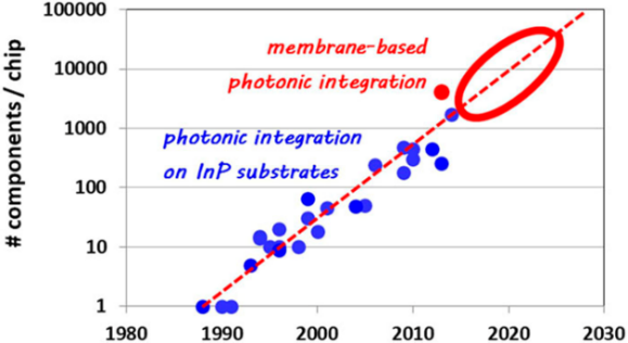
Figure 1. Moore’s law in photonics [3].
Photonic and microelectronic integration development follows the same path, with a delay of 25 to 30 years for photonics. Table 1 shows some important milestones and corresponding time nodes in the development process of the two systems.
Table 1. Milestones of microelectronic integration and photonic integration.
beginning | first integration | |
microelectronic integration | vacuum tubes ⬇ transistor (1948) | several transistors in a silicon substrate (1958) |
photonic integration | gas and solid-state lasers ⬇ semiconductor laser (1969) | a laser integrated with a modulator (1987) |
Although the development of photonic integration is later than that of electronic integration, at present, its unique and unprecedented superior performance is attracting more and more investment and research. Table 2 lists some current bottlenecks of IC and the corresponding advantages of PIC [4].
Table 2. Dilemmas of IC and advantages of PIC.
integrated circuit | approach its physical limits | high power consumption | unbalanced development of processor and memory | lower and lower cost performance |
photonic integrated circuit | fast corresponding time | low energy consumption | robust storage and computing capabilities | strong parallel and interconnect capabilities |
In fact, photonics as a parallel science with electronics itself has a lot in common, and Table 3 shows the elemental composition of the two sciences. Now that electronic circuits can be integrated, optical circuits can also be integrated. Moreover, because photons have far more exotic properties in physics than electrons, the realization of photonic integrated circuits will significantly promote the technological revolution.
Table 3. Main components of electronics and photonics.
electronics | electrons | cables and circuits | generator | electronic switch & electronic transistor |
photonics | photons | light waveguides and optical fibers | laser emitter | photoelectric modulation element |
3. Existing/Potential applications
At present, pure photonic devices can be used as independent function modules, but they are difficult to achieve complete and independent functions by themselves. Optical signal control and information storage still need to be realized by electronic devices. Therefore, a pure “photonic chip” in the perfect sense is still in the conceptual stage and has not yet formed a practical system. Strictly speaking, the practical “photonic chip” refers to the photoelectric fusion chip integrated with photonic devices or photonic functional units. Optoelectronic chips are currently mainly used in the field of communication. Other fields, such as optical computing and optical quantum, are still in the laboratory research stage, but they are likely to become disruptive technologies in the future.
3.1. Optical communication
With the rapid development of 5G, the Internet of Things, and data centers, the channel capacity of optical communication systems has increased by nearly five orders of magnitude in the past 30 years, and the current 400Gbit/s optical communication chips are being deployed in the commercial industry [5]. In remote communication using optical fiber, the optoelectronic chip plays the role of transmitting and receiving at both ends of the optical fiber. In short-range communication, optoelectronic chips are mainly used in the interconnection between different servers in data centers and in high-performance computing. With its natural advantages, the spatial structure dimension of the light wave can be combined with other multi-dimensional resources such as the wavelength, polarization, time, and complex amplitude of the light wave, so its communication capacity will be dramatically increased. Through single-chip integrated microelectronic circuits, silicon-based photonic chips can realize high-speed, high-bandwidth, low-power, low-delay on-chip interconnection while reducing the number of devices on the chip and improving the interconnection density, breaking through the current limitations of microelectronic chips in data interconnection.
Silicon-based optical communication and optical interconnection chips face three main challenges: (1) on-silicon light source. On-chip light sources can improve optical interconnection Network integration and energy utilization efficiency, and the problem of the light source is the main challenge of the whole silicon-based optoelectronics technology. Currently, the relatively mature on-chip silicon light source is based on Ⅲ-Ⅴ group materials, and the Ⅲ-Ⅴ group laser is realized on the silicon-based photonic chip by hybrid or heterogeneous integration. (2) The modulation bandwidth caused by the carrier dispersion effect is limited. The use of new modulation mechanisms, such as lithium niobate, is expected to solve this problem. (3) Large-scale integration and reliable packaging. At present, co-packaging technology can be used to enhance large-scale integration capabilities [6]. As these problems are solved one by one, the functions of silicon-based photonic integrated chips will gradually develop from fixed functions to tunable, reconfigurable, programmable, and finally realize the high intelligence of the chip to deal with more complex tasks.
3.2. Optical computing
Artificial intelligence, neural networks, speech processing, image recognition and other technologies have flourished in recent years. At the same time, large-capacity real-time data processing and analysis scenarios have spawned a fierce demand for computing power. Optical neural networks and high-performance computing based on silicon-based photonic chips are expected to solve the problems of low speed and high energy consumption of traditional microelectronic chips. Artificial neural networks can be used as data processing tools for artificial intelligence, and their calculations focus on many matrix operations. In contrast, optical neural networks consume almost no energy in these operations. At present, various structures have been used to implement on-chip deep neural networks or simulate actual brain neural network structures, all of which have achieved good results, which has strongly promoted the development of artificial intelligence [7].
In 2021, Xizhi Technology released a photonic computing processor that integrates silicon photonic chips and microelectronic chips and integrates more than 10,000 photonic devices in the photonic chip, including a 64×64 optical matrix, which is hundreds of times faster than the current high-end GPU in the calculation speed of a single problem. Although the silicon-based photonic chip is superior to the traditional microelectronic core in computing speed and power consumption, it still has some shortcomings in the all-optical realization of the nonlinear activation function of the neural network, the integration degree, and the matching algorithm of photonic chip.
The energy efficiency of optoelectronic chips is generally fJ/MAC level, which has more than two orders of magnitude advantage compared with pJ/MAC level of general microelectronic chips. At the algorithm level, academia and industry have begun to lay out the algorithm ecosystem, and breakthroughs have been made in online training algorithms. However, the optical computing chip is still far from the maturity of the electronic chip ecosystem, and its practical application still faces significant challenges. At present, some representative advances include the acceleration of optoelectronic hybrid computing and large-scale photonic computing engines, which verify the superiority of photonic computing and also show the integration and cooperation of photonic chips and traditional electronic chips [8].
3.3. Photonic quantum
Optical quantum chips use waveguides to guide photons, providing phase-stable quantum loops with core functions, including quantum state generation, manipulation, and single photon detection. Compared with traditional desktop optics, optical quantum chips make use of silicon photonic platform passive low loss, multi-dimensional to regulate device library, easy to large-scale integration, is expected to have hundreds or thousands of photons of large-scale quantum information processing, which can quickly push into the practical use of optical quantum technology. In recent years, optical quantum chips have been rapidly developed, which is expected to promote the development of quantum computing, quantum communication, quantum sensing, quantum simulation, and basic science.
Over the years, important progress has been made in the research of integrated optical quantum chips. In 2022, the Xanadu team in Canada collaborated with the National Institute of Standards and Technology in the United States to develop a programmable optical quantum chip Borealis and prove the superiority of quantum computing [9]. In 2023, the research group of Peking University and collaborators developed a wafer-level large-scale integrated silicon-based optical quantum chip preparation technology and quantum control method based on the complementary metal oxide semiconductor process and developed a very large-scale optical quantum chip integrating about 2,500 components, realizing the optical quantum computing and information processing functions based on graph theory [10]. In the same year, based on the optical quantum integrated chip, Ren Xifeng and MarioKrenn demonstrated the interference of the four-photon nonlinear generation process for the first time globally [11]. Furthermore, higher-dimensional entangled light quantum chips are beginning to explore some previously unexplored quantum applications, such as quantum randomness extension and self-testing of multi-dimensional states, which shows great potential for integrating high-dimensional entangled light quantum chips [12].
The future development trend of optical quantum chips is mainly to improve the large-scale integration and programmability of optical quantum information processing chips and expand the multi-qubit control and information processing capabilities of optical quantum chips.
4. Challenge and prospect
4.1. Large-scale photonic integration technologies
At present, depending on whether the materials and manufacturing processes of the components installed on the same substrate are the same, PIC can be divided into hybrid integration and monolithic integration [13]. The mature material systems of monolithic integration include silicon-based materials and indium phosphide materials. Table 4 compares the characteristics of these integration technologies.
Table 4. Comparison of main integration technologies for PIC.
integration technology subject | hybrid integration | monolithic integration | |
Ⅲ-Ⅴ InP | silicon-based photonic | ||
advantage | take advantage of various materials & improve performance & combine passive optical waveguide with active device | realization of active devices | compatible with CMOS & low cost & large-scale integration of passive devices |
compact structure & small size & low power consumption & high reliability | |||
defect | complex package & high cost & low integration | expensive & difficult to integrate on a large scale | difficult to integrate active devices |
Now, the main reason the integration degree of optoelectronic integrated devices is far less than that of micro-electronic devices is that there is no standardized integration technology and production line that can achieve large-scale PIC integration in line with market demand. In view of the massive investment in optoelectronic integration platforms, one solution is to mimic microelectronics foundry platforms in the field of optoelectronics. These foundry platforms achieve process scale through open multi-project wafer (MPW) streaming services, and designers only need to follow the design rules with much less time and money provided by the foundry platform [14].
Of course, real improvement also requires technological breakthroughs and innovation. The Photonic wire bonding technology proposed by researchers at the Karlsruhe Institute of Technology in Germany in 2012 can realize the interconnection between optical chips, chips, and optical fibers. Its performance index is continuously improved in continuous research, and it further realizes the miniaturization and high integration of photonic components [15]. Besides, using a femtosecond laser with high precision and intense penetration as a sharp tool, an arbitrary three-dimensional polymer structure is directly written inside the photoresist, and unique optical components are designed according to the characteristics of the chip itself. This technique, called Photonic Wire Bonding(PWB), can significantly simplify the traditional optical high-precision alignment assembly technology and can realize maskless processing, providing an innovative solution for the effective integration of optical chips [16] (see Figure 2).
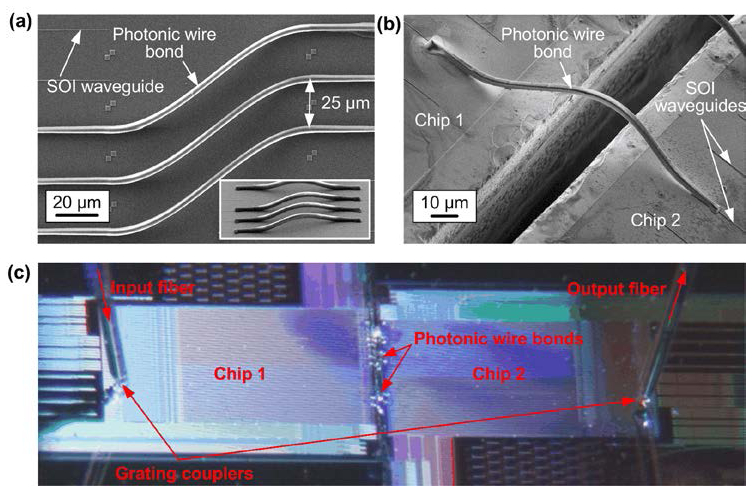
Figure 2. Photonic Wire Bonding seen at different positions. (a) PWB prototype connecting two silicon-on-insulator (SOI) waveguides on the same chip. (b) PWB chip-to-chip interconnect. (c) Optical characterization setup of a PWB assembly linking two SOI chips [17].
Besides, three-dimensional photonic integrated circuits (3D-PICs), realized by stacking multilayer photonic devices, can break through the limitations of two-dimensional planar integration and improve the integration degree of photonic chips. In 2019, a collaborative team from the University of California, Berkeley, and the Massachusetts Institute of Technology prepared a three-dimensional optoelectronic hybrid chip through a wafer bonding process, effectively avoiding the previous complex process procedures [18]. The preparation process is shown in Figure 3. After the Optical chip and electrical chip are prepared respectively, three-dimensional integration is realized through wafer bonding, and the direct control of a three-dimensional integrated Optical Phase Array (OPA) is realized by means of perforation interconnection.
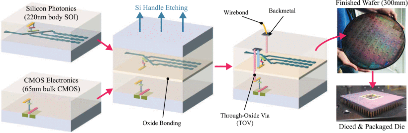
Figure 3. Overview of the 3-D heterogeneous integration platform used to construct the single-chip OPA [19].
4.2. Prospect
Due to the unique performance of photons, photon chip as an emerging technology has many advantages compared with electronic chip. It has shown great application potential in information transmission, computing, sensing, etc. However, the current photonic integration circuit is far less advanced than the electronic one, especially in large-scale integration, loss reduction, and other problems. Capacity, bandwidth density, chip size, and power efficiency are key factors to be considered in PIC design and implementation [20]. In addition, how to make the photonic integration technology learn from the development of more mature electronic integration technology to speed up its own technological breakthroughs and flexibly integrate into various daily applications, and how to make the existing photonic integration technology better cooperate and complement the electronic integration technology are also very necessary to consider. At the application level, since the thermal radiation and molecular characteristic absorption peaks of the object are located in the mid-infrared band, on-chip optoelectronic devices can provide subwavelength scale light limitation, greatly improving the light-matter interaction and signal-to-noise ratio (SNR). Therefore, extending the operating wavelength of integrated photonic devices and systems to the mid-infrared will be a disruptive technology and provide significant development opportunities for future mid-infrared optoelectronic systems and applications [21].
In general, it has become an important development trend to develop multi-material systems and corresponding processes, further miniaturize photonic devices to achieve integration with electronic devices, and give full play to the advantages of high speed, high bandwidth, low energy consumption, multi-dimensional multiplexing of photonic technology and the advantages of microelectronic technology in nonlinear manipulation and functional diversity. In order to meet the development needs of future ultra-large-scale photonic integration, we need to start from the source innovation of unit device principle, material, and structure and actively promote the standardization, automation, and intelligent development of chip design and manufacturing through cross-field strong joint.
5. Conclusion
Photonic and electronic integration have similar development tracks, and there are indeed corresponding and complementary relations between them in many aspects, which points out the certainty and direction for the rapid development of photonic chips in the future. Although only a few mature photonic chips can be applied to optical communication and optical interconnection for the moment, many research advances in optical computation and optical quantum still indicate the unprecedented value of photonic integration. At present, integrating photonic devices in a large range is one of the main challenges in this field. The existing monolithic and hybrid integration technologies have advantages and disadvantages, and their comprehensive application needs further improvement. The photonic wire bonding technology and three-dimensional photonic integrated circuits, which have attracted much attention, may become an effective means to improve the integration degree.
References
[1]. Miller, S. E. (1969) Integrated optics: An introduction. Bell Syst. Tech., 48: 2059–2069. https://doi.org/10.1002/j.1538-7305.1969.tb01165.x.
[2]. Tien, P. K. (1977) Integrated optics and new wave phenomena in optical waveguide. Rev. Mod. Phys., 49(2): 361–420. https://doi.org/10.1103/revmodphys.49.361.
[3]. Smit, M., Williams, K., Tol, J. (2019) Past, present, and future of InP-based photonic integration. APL Photonics, 4(5): 050901.
[4]. Mi, L. (2022) Layout photonic chips with the strategic vision of scientific and technological revolution. Outlook Weekly. http://lw.news.cn/2022-01/10/c_1310416707.htm.
[5]. Li, D., Xu, P., Zhu, K., Zhou, Z. (2021) Applications and challenges of silicon-based optoelectronics in communication. Telecommunications Science, (10): 1-11.
[6]. Ma, H., Li, X., Wang, Y., Yang, J. (2022) Progresses and Challenges of Silicon-based Photonic Chips. Semiconductor Optoelectronics, 43(2): 218-227.
[7]. Bai, B., Pei, L., Zuo, X. (2021) Silicon Photonic Chips for Artificial Intelligence. ZTE Technology Journal, 27(1): 77-82.
[8]. Gong, Q.H., Xiao, Y.F., Luo, X. et al. (2023) Nano-optoelectronics and Photonic Chips: Progresses and Challenge. Bulletin of National Natural Science Foundation of China, 37(3): 410-417.
[9]. Madsen L. S., Laudenbach F., Askarani M. F., et al. (2022) Quantum computational advantage with a programmable photonic processor. Nature, 606: 75-81.
[10]. Bao, J. M., FU, Z. R., Pramanik, T., et al. (2023) Very-large-scale integrated quantum graph photonics. Nature Photonics, 17: 573-581.
[11]. Feng, L.T., Krenn, M., Ren, X.F., et al. (2023) On-chip quantum interference between the origins of a multi-photon state, Optica, 10(1): 105-109.
[12]. Chen, Z.Y., Lu, L.L. (2022) High⁃dimensional integrated quantum photonic technology. Journal of Nanjing University(natural science), 58(2):183-192.
[13]. Shen, X., Yu J.P., Wang, L. (2023) Research Focus and Trend in Photonic Chip. Frontiers of Data & Computing, 5(4): 3-15.
[14]. Zheng, X., Liu, Y. (2017) Large-scale Photonic Integration Technologies Based on Multi-Project Wafer Flow Sheet. Laser & Optoelectronics Progress, 54(5): 050001.
[15]. Zhang, X. S., Kwon, K., Henriksson, J., et al. (2022) A large-scale microelectromechanical-systems-based silicon photonics LiDAR. Nature, , 603: 253-258.
[16]. Zhao, Y., Lin, L.H., Sun, H.B. (2022) On-chip Optical Interconnection Based on Two-photon Polymerization (Invited). Acta Photonica Sinica, 51(8): 0851512.
[17]. Lindenmann N., Balthasar G., Hillerkuss D., Schmogrow R., Jordan M., Leuthold J., Freude W., and Koos C. (2012) Photonic wire bonding: a novel concept for chip-scale interconnects. Opt., 20(16): 17667-17677.
[18]. Yin Y.X., XU, X.R., Ding, Y.Z., et, al. (2022) Progress and Challenge of 3D Photonic Integrated Circuit (Invited). Acta Photonica Sinica, 51(7): 0751416.
[19]. Zhang, X. S., Kwon, K., Henriksson, J., et al. (2022) A large-scale microelectromechanical-systems-based silicon photonics LiDAR. Nature, 603:253-258.
[20]. Su Y.K., He, Y., Guo, X.H., Xie, W.Q., et al. (2023) Scalability of Large-Scale Photonic Integrated Circuits. ACS Photonics, 10(7): 2020-2030.
[21]. Lin, H.T., Sun, B.S., Ma, H., et al. (2022) Review of mid-infrared on-chip integrated photonics (Invited). Infrared and Laser Engineering, 51(1): 20211111.
Cite this article
Zhang,P. (2024). Development and application prospect of photonic integrated circuits. Applied and Computational Engineering,84,146-153.
Data availability
The datasets used and/or analyzed during the current study will be available from the authors upon reasonable request.
Disclaimer/Publisher's Note
The statements, opinions and data contained in all publications are solely those of the individual author(s) and contributor(s) and not of EWA Publishing and/or the editor(s). EWA Publishing and/or the editor(s) disclaim responsibility for any injury to people or property resulting from any ideas, methods, instructions or products referred to in the content.
About volume
Volume title: Proceedings of the 4th International Conference on Materials Chemistry and Environmental Engineering
© 2024 by the author(s). Licensee EWA Publishing, Oxford, UK. This article is an open access article distributed under the terms and
conditions of the Creative Commons Attribution (CC BY) license. Authors who
publish this series agree to the following terms:
1. Authors retain copyright and grant the series right of first publication with the work simultaneously licensed under a Creative Commons
Attribution License that allows others to share the work with an acknowledgment of the work's authorship and initial publication in this
series.
2. Authors are able to enter into separate, additional contractual arrangements for the non-exclusive distribution of the series's published
version of the work (e.g., post it to an institutional repository or publish it in a book), with an acknowledgment of its initial
publication in this series.
3. Authors are permitted and encouraged to post their work online (e.g., in institutional repositories or on their website) prior to and
during the submission process, as it can lead to productive exchanges, as well as earlier and greater citation of published work (See
Open access policy for details).
References
[1]. Miller, S. E. (1969) Integrated optics: An introduction. Bell Syst. Tech., 48: 2059–2069. https://doi.org/10.1002/j.1538-7305.1969.tb01165.x.
[2]. Tien, P. K. (1977) Integrated optics and new wave phenomena in optical waveguide. Rev. Mod. Phys., 49(2): 361–420. https://doi.org/10.1103/revmodphys.49.361.
[3]. Smit, M., Williams, K., Tol, J. (2019) Past, present, and future of InP-based photonic integration. APL Photonics, 4(5): 050901.
[4]. Mi, L. (2022) Layout photonic chips with the strategic vision of scientific and technological revolution. Outlook Weekly. http://lw.news.cn/2022-01/10/c_1310416707.htm.
[5]. Li, D., Xu, P., Zhu, K., Zhou, Z. (2021) Applications and challenges of silicon-based optoelectronics in communication. Telecommunications Science, (10): 1-11.
[6]. Ma, H., Li, X., Wang, Y., Yang, J. (2022) Progresses and Challenges of Silicon-based Photonic Chips. Semiconductor Optoelectronics, 43(2): 218-227.
[7]. Bai, B., Pei, L., Zuo, X. (2021) Silicon Photonic Chips for Artificial Intelligence. ZTE Technology Journal, 27(1): 77-82.
[8]. Gong, Q.H., Xiao, Y.F., Luo, X. et al. (2023) Nano-optoelectronics and Photonic Chips: Progresses and Challenge. Bulletin of National Natural Science Foundation of China, 37(3): 410-417.
[9]. Madsen L. S., Laudenbach F., Askarani M. F., et al. (2022) Quantum computational advantage with a programmable photonic processor. Nature, 606: 75-81.
[10]. Bao, J. M., FU, Z. R., Pramanik, T., et al. (2023) Very-large-scale integrated quantum graph photonics. Nature Photonics, 17: 573-581.
[11]. Feng, L.T., Krenn, M., Ren, X.F., et al. (2023) On-chip quantum interference between the origins of a multi-photon state, Optica, 10(1): 105-109.
[12]. Chen, Z.Y., Lu, L.L. (2022) High⁃dimensional integrated quantum photonic technology. Journal of Nanjing University(natural science), 58(2):183-192.
[13]. Shen, X., Yu J.P., Wang, L. (2023) Research Focus and Trend in Photonic Chip. Frontiers of Data & Computing, 5(4): 3-15.
[14]. Zheng, X., Liu, Y. (2017) Large-scale Photonic Integration Technologies Based on Multi-Project Wafer Flow Sheet. Laser & Optoelectronics Progress, 54(5): 050001.
[15]. Zhang, X. S., Kwon, K., Henriksson, J., et al. (2022) A large-scale microelectromechanical-systems-based silicon photonics LiDAR. Nature, , 603: 253-258.
[16]. Zhao, Y., Lin, L.H., Sun, H.B. (2022) On-chip Optical Interconnection Based on Two-photon Polymerization (Invited). Acta Photonica Sinica, 51(8): 0851512.
[17]. Lindenmann N., Balthasar G., Hillerkuss D., Schmogrow R., Jordan M., Leuthold J., Freude W., and Koos C. (2012) Photonic wire bonding: a novel concept for chip-scale interconnects. Opt., 20(16): 17667-17677.
[18]. Yin Y.X., XU, X.R., Ding, Y.Z., et, al. (2022) Progress and Challenge of 3D Photonic Integrated Circuit (Invited). Acta Photonica Sinica, 51(7): 0751416.
[19]. Zhang, X. S., Kwon, K., Henriksson, J., et al. (2022) A large-scale microelectromechanical-systems-based silicon photonics LiDAR. Nature, 603:253-258.
[20]. Su Y.K., He, Y., Guo, X.H., Xie, W.Q., et al. (2023) Scalability of Large-Scale Photonic Integrated Circuits. ACS Photonics, 10(7): 2020-2030.
[21]. Lin, H.T., Sun, B.S., Ma, H., et al. (2022) Review of mid-infrared on-chip integrated photonics (Invited). Infrared and Laser Engineering, 51(1): 20211111.