


1. Introduction
Universal Asynchronous Receiver/Transmitter (UART) is a universal serial, asynchronous, full-duplex communication protocol commonly used to implement data transmission in embedded and IoT systems. In modern computer systems, UART is used widely thanks to its simple structure and long transmission distance [1]. It is often used as a connection between computers and external devices, such as sensors, monitors, printers, etc., that transmit data using serial communication [2], and has a wide range of applications in the internal communication of on-board instruments [3]. Common UART dedicated chips that convert parallel data of the computer and serial data from peripherals, like 8250, 8251, and NS6450, are more complex and are difficult to meet the current high-speed data transmission occasions [4]. Therefore, it is of great practical significance to study and design the hardware implementation based on the UART protocol, which can solve the problem of resource wastage of the traditional UART and can make the whole design more stable and reliable, reduce the board area and simplify the circuit [5,6].
Field Programmable Gate Array (FPGA) is an integrated circuit device, built on the basis of programmable devices [2]. It has wide popularity in the field of electronics and is usually used for advanced hardware design and verification, allowing various functions to be implemented at the hardware level. As a semi-custom circuit, compared with the traditional ASIC design method, it overcomes the disadvantage of immutable custom circuits to a certain extent and reduces the cost. At the same time, it solves the problems of the small number of gates and simple functions of the original programmable devices [7]. It has the advantage of high flexibility and reconfigurability and is well-suited for developing and verifying hardware implementations of communication protocols. Furthermore, FPGAs have programmable logic components called ‘logic blocks’ and a hierarchy or reconfigurable interconnects which facilitate the wiring of the blocks together. Asynchronous serial communication can be implemented easily on FPGA [8].
The study of the hardware implementation of the transmitter and receiver based on the UART protocol is important in several ways. By optimizing and improving the hardware implementation of the UART communication protocol, the speed and stability of data transmission can be increased and the efficiency of communication can be improved. By checking the waveforms, the reliability of the communication protocol can be verified to ensure the accurate transmission and reception of the communication data. The UART communication protocol has unique advantages in some specific application scenarios, and the study of the hardware implementation can help to explore the application prospects of asynchronous communication. By synthesizing the transmitter and receiver side hardware modules based on the UART protocol on FPGAs, the correctness and performance of the hardware design can be verified, and possible problems and defects can be identified and solved.
Therefore, it is important to study the hardware implementation of transmitter and receiver based on UART protocol to promote the application and development of communication protocols in FPGAs. It helps to improve communication efficiency, verify the reliability of the communication protocol, and explore the potential of asynchronous communication.
The aim of this paper is to design and implement a hardware module on an FPGA chip for data transfer between two devices using the UART communication protocol. The receiver device acts as the data receiver and converts the serial data into parallel data. The transmitting device acts as the data sender and reverses the previous process, converting the parallel data into serial data and sending it out. In this study, the two achieve data transfer and interaction to verify data accuracy through parallel data communication. The tools used in this study mainly include FPGA development-related software, such as ModelSim, Quartus, and the hardware description language Verilog HDL, to carry out the hardware circuit design, simulation, programming, and testing of data transmission for the UART interface. This hardware implementation aims to validate the reliability and practicality of the UART communication protocol in FPGAs, as well as to explore the problems and challenges that may be encountered in practical applications.
2. UART communication principle analysis
The transmitter sends data at a specific frame. As shown in Fig 1, it first sends binary 0 as the start bit. The start bit is used to alert the receiver that a word of data is about to be sent and to force the clock in the receiver to synchronization with the clock in the transmitter then sends an 8-bit data bit [8], when the receiver has received all of the data bits, it may check for the Parity Check Bit (both transmitter and receiver must agree on whether a Parity Check Bit is to be used), and then the receiver looks for a Stop Bit [9]. This forms the frame for the UART communication transmission. Note that serial data is sent first with the low bit of the data, which is bit 0, and last with bit 7.
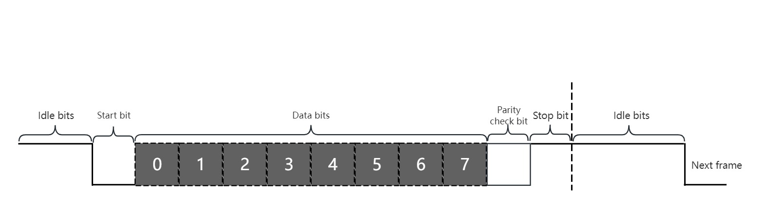
Figure 1. UART frame.
3. FPGA hardware implementation
3.1. Design idea
UART is a universal asynchronous serial communication protocol that enables interconversion between serial and parallel data. In FPGAs, this conversion has to be done at a uniform baud rate. So, in the design of the hardware circuit, a uniform clock signal as well as a baud rate clock generation module is required for the generation of bit signals at a specific baud rate. The receiver receives the serial data from RXD, reads it in and converts it into 8-bit parallel data after removing the start and end bits, and finally converts it into data that can be processed by the receiving device. When the transmitter receives the 8-bit parallel data, it converts it into serial data TXD after packing it with the start bit, end bit, and parity check bit, and then sends it out.
3.2. External signal definition
Table 1. External signal definition.
Signal Name | Signal Type |
CLK | Input |
RST | Input |
RXD | Input |
TXD | Output |
Tx_enable | Input |
As shown in Table 1, all external signals for this design are shown. CLK is the clock signal with a frequency of 50MHz. RST is the asynchronous reset signal, active low. RXD is the input serial signal. TXD is the output serial signal. Tx_enable is the synchronous TXD enable signal. TXD starts to output data when the rising edge of the clock arrives and the signal Tx_enable is high.
3.3. Submodule design
The first step is to design a general framework, which will contain three sub-modules, namely the data receiving module, the data transmitting module and the baud rate clock generator module. The baud rate clock generation module is actually a frequency divider that uses a counter to convert the input clock signal into a baud rate clock signal [10], which is connected to the data receiving, and transmitting module through a serial port. The data receiving, and transmitting module will operate at this baud rate clock for serial, parallel data conversion to each other. With this modular design and serial connection mode, future maintenance and porting can be simplified.
A schematic of the overall design is shown in Fig 2.
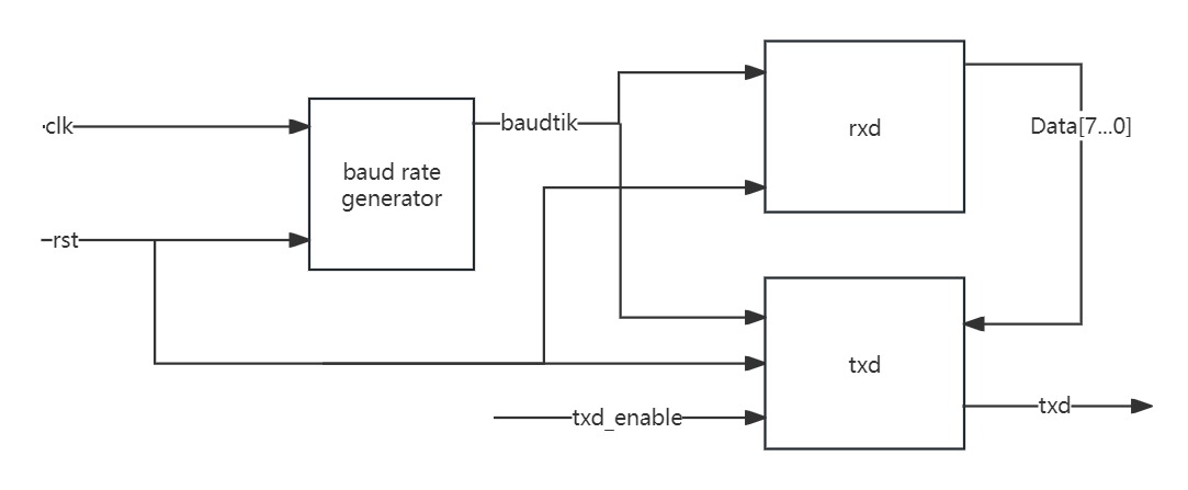
Figure 2. Combined diagram.
3.3.1. Baud rate clock generation module. The baud rate describes the speed at which data can be transmitted, i.e. how many bits of binary data can be transmitted per second. In UART communication, the commonly used baud rates are 9600, 19200, 38400 and 115200bps. To ensure that data is transmitted and received correctly, a baud rate synchronized clock matching the RS-232 standard must be generated [2]. An accurate selection of sampling points is required, both in the UART receiver and transmitter. The baud rate clock can be implemented by designing a counter. In addition to this, since in reality data signals are usually not idealized square wave signals, but rather have ‘burrs’, it is best to sample the data at the midpoint of each bit of the serial data. This design uses a baud rate of 115200bps as an example. When the baud rate is 115200bps, 115200 bits of data are transmitted per second, then the data transmission time per bit is 1/115200 seconds. When the main clock is 50MHz, it takes 433 counts to transmit each bit. When the serial signal is sent to the start bit to start counting, counting to 216, the baudtick signal will be pulled high, and thereafter every count of 433 times to pull up the baudtick signal, at this point in time for the data sampling will be able to ensure that in the mid-point of the data to be sampled.
3.3.2. Data receiving module. The module uses baudtick as the sampling clock for the midpoint of the data bits, RXD represents the received serial data, and rxd_data is the received data register to store the parallel data. rxd_busy indicates that data is currently being received. baudtick_start indicates that the start bit is received to start the baud rate clock. In order to avoid ‘burrs’ in the start bit, four shift registers, rxd0, rxd1, rxd2, rxd3, are used to check if the data is really a falling edge. When the start bit is received, the data reception starts by pulling up the logic level of the baudtick_start and rxd_busy signals at this time. When reception is complete, baudtick_start and rxd_busy are to be set low. rxd_data[7:0] is the parallel data that converted from serial data and used to pass to the receiving device.
3.3.3. Data transmitting module. The transmitter and receiver modules are functionally similar. The transmit module converts 8-bit serial input data to serial output. In this case, txd_data[7:0] contains the parallel data to be sent. baudtick and baudtick_start function the same as the receive module. When Tx_enable is set high, it indicates the start of sending data. During data transmission, tx_busy remains high at all times. After adding the start bit, parity check bit and end bit, tx_busy is set low and the serial data signal TXD is sent.
4. Tests and results
4.1. Waveform inspection
4.1.1. Data receiving module. As shown in Fig 3, the baud rate clock starts after half a cycle when the falling edge of the incoming serial signal RXD is detected, ensuring that the sampling point is located on the midpoint of the data. The parity check bit and stop bit are detected after the 8-bit data is captured, and then the baud rate clock ends. Notice that the input RXD is 01101110011, after detecting the start bit 0, even parity check bit 1 and stop bit 1 to judge the UART format is correct, at this time the data bit 11011100 is stored. The final output of the parallel data rxd_data is in the opposite direction to the serial data, verifying its compliance with the UART communication protocol. It can also be noticed that baudtick_start and rxd_busy are always high during data reception. The data receiving module is designed as expected and the functionality check is intact.
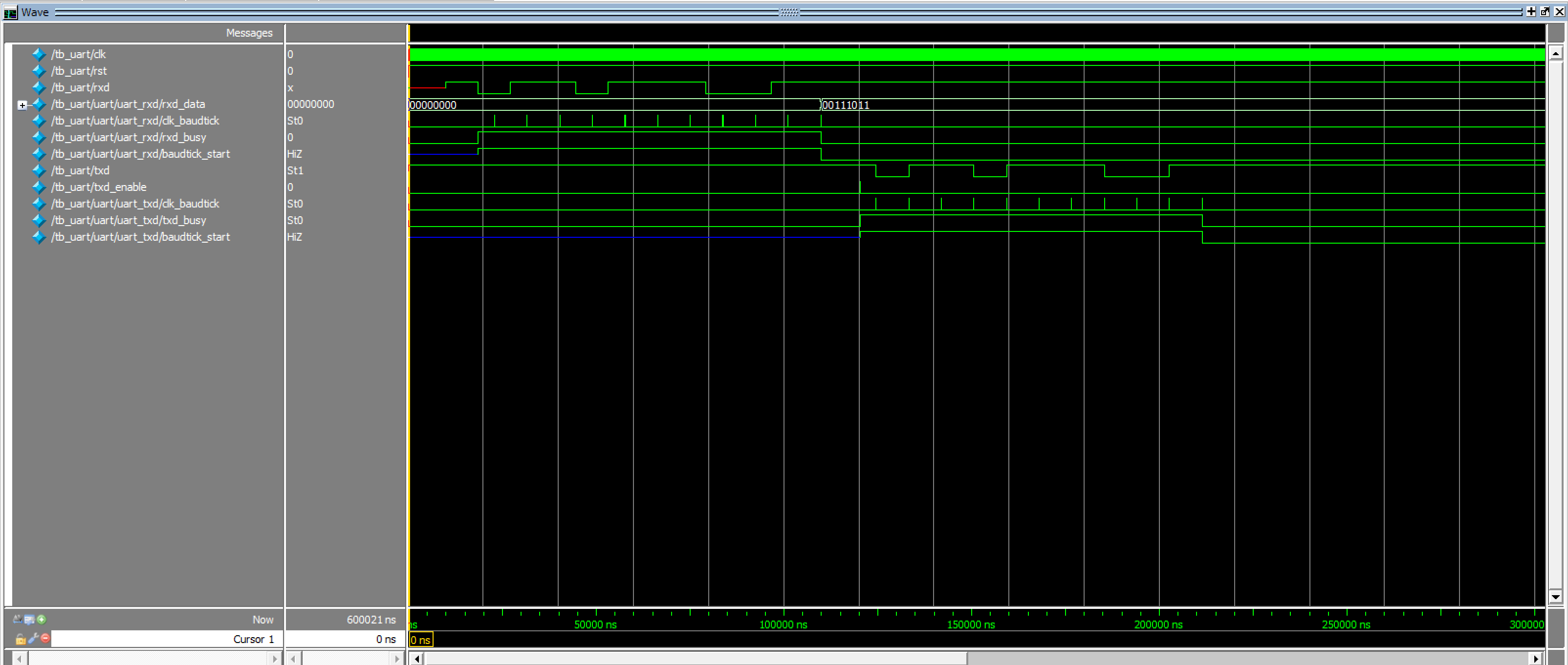
Figure 3. Data receiving module simulation waveform.
4.1.2. Data transmitting module. As shown in Fig 4, txd_busy and baudtick_start are pulled up quickly after the arrival of Tx_enable, and the parallel data 00111011 is inverted, packed with the start bit, and parity check bit, and sent out. Since both the stop bit and the idle bit are logic-high, the baud rate clock can be stopped after sending the parity check bit. At this point, txd_busy and baudtick_start pull down quickly. Since the same parallel data is used, we can find that the RXD and TXD waveforms match and are both 01101110011, which verifies their compliance with the UART communication protocol. The data transmitting module is designed as expected and the function check is complete.

Figure 4. Data transmitting module simulation waveform.
4.2. System RTL simulation diagram and performance analysis
The RTL scheme is the system logic that will be implemented. Simulation testing of the hardware circuit in the Quartus II simulator as shown in the block diagram in Fig 2 will produce the entire system as shown in the schematic in Fig 5. Make sure that the corresponding hardware circuit can be generated and the performance meets the requirements of the UART protocol.
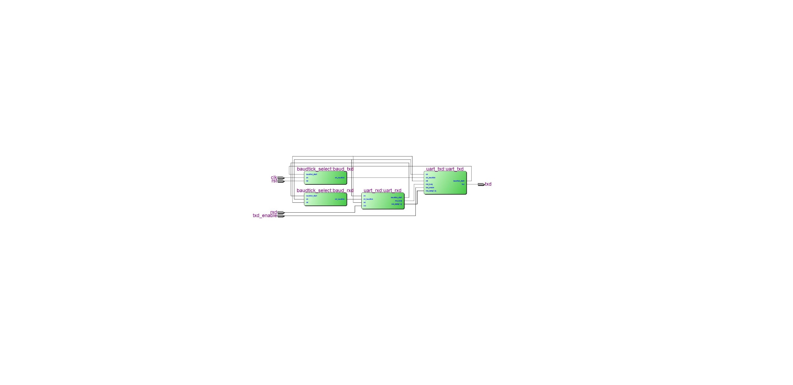
Figure 5. RTL schematic of system.
As shown in Fig 6, the design as a whole uses a relatively small number of logic devices, requiring only 109 logic devices to complete the hardware circuit implementation of the transmitter and receiver based on the UART protocol.
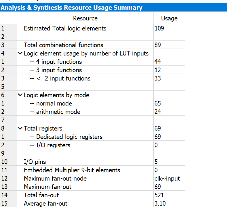
Figure 6. Analysis and Synthesis resource usage summary.
As shown in Fig 7, the maximum frequency is 389.11MHz at Slow 1200mV 85 degrees Celsius, which is faster. At the same time, the operation frequency is greater than the clock frequency and the timing can run correctly. The clock frequency also has room to grow, which can further speed up the transmission rate.
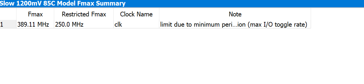
Figure 7. Slow 1200mV 85C model max summary.
5. Conclusion
Through practical tests and analyses, it is verified that the UART protocol implemented based on FPGA has a fast data transmission rate, stable performance, correct communication timing and reliable data transmission. At the same time, due to the design of the serial data sampling at the midpoint, greatly avoiding the impact of the real data in the ‘burr’, improve the reliability of the transmission data. Ultimately, the design proved to be effective, integrable, and stable enough to be used in practical applications.
However, there are still numerous shortcomings in the current study. Some redundant signals could be further streamlined. This design uses two baud rate clock generation modules to ensure stability. In the future, we can try to combine them into one to further streamline the system and improve the operation frequency and transmission rate.
Since the baud rates used by different communication devices are different, in the future, this study can design a module that can automatically detect the communication baud rate and generate the corresponding baud rate clock by passing the parameters to the baud rate clock generator module, which can further expand its applicable fields. At the same time, an infinite increase in transmission rate is not possible due to the marginal effect of boosting the design's computing frequency. In the future, it will be possible to split the data, synchronize the data transfer by multiple UART modules and finally assemble them. This method can further enhance the transmission rate, break through the existing limitations, promote the advancement of data transmission technology, extend to a wider range of applicable fields, and bring more benefits to human society.
References
[1]. Govil A Karnwal A Sindhu G Singh A Shukla S 2022 Design and Implementation of UART Using FPGA Board. International Journal for Research in Applied Science Engineering Technology
[2]. Tang M 2013 UART module design based on FPGA and PC serial communication Huazhong Normal University
[3]. Chen R Wang H 2015 Design and implementation of spaceborne UART communication based on FPGA Science and Engineering vol 15 no 13 p 212-217
[4]. Liu B 2018 Design and implementation of UART module based on FPGA Radio Engineering, vol 48 no 05 p 433-438
[5]. Shi G Shi X Zuo X 2009 Design and implementation of UART based on FPGA China New Communications vol 11 no 07 p 62-65
[6]. Jia L Ji Y 2016 Design of serial communication controller based on FPGA Microcomputer and application vol 35 no 22 p 33-35 + 39
[7]. Wang Ch 2003 People 's Post and Telecommunications Publishing House. FPGA / CPLD design tool
[8]. Dakua B R Hossain M I Ahmed F 2015 Design and implementation of UART serial communication module based on FPGA. Design And Implementation of UART Serial Communication Module Based on FPGA.
[9]. Irfansyah S 2019 Design and Implementation of UART With FIFO Buffer Using VHDL On FPGA. ICTACT J. Microelectron vol 5 no 01 p7
[10]. Xie X 2012 UART design based on FPGA Electronic Design Engineering vol 20 no 16 p 51-53
Cite this article
Xing,Y. (2024). Hardware circuit implementation of transmitter and receiver based on UART protocol. Applied and Computational Engineering,72,204-210.
Data availability
The datasets used and/or analyzed during the current study will be available from the authors upon reasonable request.
Disclaimer/Publisher's Note
The statements, opinions and data contained in all publications are solely those of the individual author(s) and contributor(s) and not of EWA Publishing and/or the editor(s). EWA Publishing and/or the editor(s) disclaim responsibility for any injury to people or property resulting from any ideas, methods, instructions or products referred to in the content.
About volume
Volume title: Proceedings of the 2nd International Conference on Functional Materials and Civil Engineering
© 2024 by the author(s). Licensee EWA Publishing, Oxford, UK. This article is an open access article distributed under the terms and
conditions of the Creative Commons Attribution (CC BY) license. Authors who
publish this series agree to the following terms:
1. Authors retain copyright and grant the series right of first publication with the work simultaneously licensed under a Creative Commons
Attribution License that allows others to share the work with an acknowledgment of the work's authorship and initial publication in this
series.
2. Authors are able to enter into separate, additional contractual arrangements for the non-exclusive distribution of the series's published
version of the work (e.g., post it to an institutional repository or publish it in a book), with an acknowledgment of its initial
publication in this series.
3. Authors are permitted and encouraged to post their work online (e.g., in institutional repositories or on their website) prior to and
during the submission process, as it can lead to productive exchanges, as well as earlier and greater citation of published work (See
Open access policy for details).
References
[1]. Govil A Karnwal A Sindhu G Singh A Shukla S 2022 Design and Implementation of UART Using FPGA Board. International Journal for Research in Applied Science Engineering Technology
[2]. Tang M 2013 UART module design based on FPGA and PC serial communication Huazhong Normal University
[3]. Chen R Wang H 2015 Design and implementation of spaceborne UART communication based on FPGA Science and Engineering vol 15 no 13 p 212-217
[4]. Liu B 2018 Design and implementation of UART module based on FPGA Radio Engineering, vol 48 no 05 p 433-438
[5]. Shi G Shi X Zuo X 2009 Design and implementation of UART based on FPGA China New Communications vol 11 no 07 p 62-65
[6]. Jia L Ji Y 2016 Design of serial communication controller based on FPGA Microcomputer and application vol 35 no 22 p 33-35 + 39
[7]. Wang Ch 2003 People 's Post and Telecommunications Publishing House. FPGA / CPLD design tool
[8]. Dakua B R Hossain M I Ahmed F 2015 Design and implementation of UART serial communication module based on FPGA. Design And Implementation of UART Serial Communication Module Based on FPGA.
[9]. Irfansyah S 2019 Design and Implementation of UART With FIFO Buffer Using VHDL On FPGA. ICTACT J. Microelectron vol 5 no 01 p7
[10]. Xie X 2012 UART design based on FPGA Electronic Design Engineering vol 20 no 16 p 51-53