


1. Introduction
With the rapid development of modern electronic technology, the importance of high-performance amplifiers in fields such as communications, signal processing, and radio frequency has become increasingly significant. The cascode amplifier has become the first choice for many high-frequency applications due to its high gain and wide bandwidth characteristics. In addition to multi-stage amplifiers, the cascode amplifiers have two structures: folded-cascode amplifiers and telescopic operational amplifiers, both of which have the characteristics of high swing and low power consumption. Semiconductor giants such as TSMC and Intel have begun researching production processes of 2, 3 nanometres and China has also completed 14-nanometer chip design.
The cascode circuit can be said to be a key part of CMOS. However, how to improve its gain is still a challenging topic [1, 2].
In 2022, Wang et al. proposed an accurate design method for a folded cascode operational amplifier. The traditional design of folded cascode operational amplifiers often needs people to use formulas to manually calculate parameters, and then they have to change the parameters based on actual results. Due to special circumstances such as short channel length in actual devices, the error will be large. In comparison, this method is more accurate and saves effort [3].
In 2024, Nourhan Elsayed and colleagues employed FDSOI technology associated with the stacking technique and applied it to a cascode amplifier. They designed an E-type amplifier aimed primarily at enhancing output power. By stacking multiple devices, the voltage can be significantly increased, thereby enlarging the swing. The use of a switched-cascode structure modifies the gate signal to introduce delays, altering the overlap of output voltage and current waveforms to boost power. It was ultimately found that the cascode structure increased power added efficiency (PAE) by 28%, while the switched-cascode structure improved it by approximately 35% [4].
This project investigates the gain characteristics of cascode amplifiers from both theoretical and simulation perspectives, aiming to provide a theoretical foundation and practical guidance for the design of high-performance common-source common-gate amplifiers. It also examines the impact of varying width-to-length ratios and voltage levels on the circuit, as well as the roles of different circuit components.
2. Theoretical Analysis
The Common Source Common Gate (CSCG) is a distinctive circuit structure commonly employed in RF and low-noise amplifier designs. Among various Operational Transconductance Amplifier (OTA) architectures, the folded cascode operational amplifier structure allows designers to optimize second-order performance metrics, which is a feat almost unattainable in traditional operational amplifiers. Specifically, the Common Source Common Gate technology proves effective in enhancing gain, increasing Power Supply Rejection Ratio (PSRR), and enabling self-compensation at the output stage.
The common-source common-gate amplifier is composed of a common-source stage and a common-gate stage connected in series. The common-source stage provides high input impedance and current gain, while the common-gate stage significantly enhances voltage gain by improving output impedance and mitigating the Miller effect. The gain of the common-source common-gate amplifier can be approximated by the following formula: for a typical common-source stage:
Avo = −gm* Ro. (1)
The output resistance of the common-source common-gate stage is Ro ≃ (gm2* ro2) *ro1, so the gain of the common-source common-gate stage is:
Avo = −(gm1 *ro1) *(gm2* ro2) (2)
Here, gm1 is the transconductance of the common-source transistor, and r_o1 and r_o2 are respectively the output resistances of the common-source and common-gate transistors. When these resistances are equal, the gain can even be approximated as the square of the common-source stage gain. Thus, this structure effectively amplifies gain, with the main factors affecting the gain being the transistor's transconductance, the transistor's output resistance, the load resistance (RL), and the bias current and voltage [5].
Apart from the fundamental amplifier section, the biasing circuit is also a crucial component in such operational amplifiers. The biasing circuit primarily provides appropriate bias currents to the MOS transistors in the core amplifier section, ensuring that they operate stably within the designated region. Typically, current mirrors are used to implement the bias current transfer. Additionally, biasing circuits can enhance gain and improve linearity while minimizing distortion. Through appropriate bias settings, the gain-bandwidth product of the circuit can be optimized. By maximizing the product of gain and bandwidth, the circuit maintains high gain over a wide frequency range. Furthermore, compensation circuits, often employing Miller compensation, are usually present at the output stage. These circuits work by reducing bandwidth to ensure sufficient gain and output swing, with a common approach being the use of capacitors to design the circuit, separate poles, and increase phase margin.
In 2019, Sudheer Raja et al. analysed a modified version of the recycled folded cascode OTA circuit (MRFC), designed to address the issue where the folded section of the folded cascode OTA merely serves to fold the circuit and conduct current without enhancing gain. They introduced new MOS transistors into the recycling folded cascode (RFC) OTA to modify the differential pair’s input to consist of two sets of MOS transistors with fixed width-to-length ratios and identical currents. Additionally, the current mirror transistors were increased to three sets, with two sets of MOS transistors added at the drain to stabilize the drain voltage and current. This modification effectively amplifies the transconductance while demonstrating favourable performance in terms of noise and swing [6].
In 2021, Xu investigated methods to enhance the gain of folded cascode operational amplifiers by designing and simulating a circuit structure for such amplifiers. Beyond the basic common-source cascode amplifier configuration, he incorporated constant current source output structures, common-source amplifier output structures, and biasing circuits. The results achieved a gain of 110 dB and a unit gain bandwidth of approximately 74 MHz, demonstrating a significant improvement in gain [7].
3. Simulation
3.1. Comparison between cascode circuit and common source
As shown in figure 1 below, this study established a basic common-source cascode circuit structure and used Cadence for circuit simulation, examining gain variations under different width-to-length ratios and gate voltages. Additionally, the study simulated the gain of a common-source circuit using the same input structure and conducted a comparative analysis of the differences between the circuits.
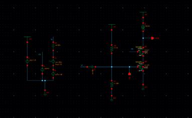
Figure 1. Basic cascode simulation circuit.
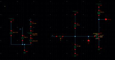
Figure 2. Basic common-source stage simulation circuit.
As shown in Figure 1 and Figure 2, a voltage source of 1.8 V is provided for VDD. The gate voltage of the common-source MOS transistor is derived from a voltage divider consisting of two resistors, while the input capacitor and resistor serve as AC coupling elements. The resistor values are 15 kΩ and 10 kΩ, respectively, with the gate voltage set to 1 V. A current source is used to simulate the load, maintaining a constant current. The width-to-length ratios of the transistors are adjusted until both operate in the saturation region, as detailed in Figure 3. Figure 4 and Figure 5 show the simulation results for the output voltage, which exhibit a significant difference, approximately 15 times. The result is consistent with the conclusions drawn earlier.
Additionally, this research attempts to vary the parameters of the MOS transistors. Likewise, it examines the impact of different width-to-length ratios on the device's operating region and output characteristics. Keeping other parameters constant, several situations were tested: both transistors with a width-to-length ratio of 1 µm to 180 nm, a common-source transistor with a ratio of 1.2 µm to 180 nm, and a common-gate transistor with a ratio of 5 µm to 180 nm. Since the load is a current source, the drain current is fixed. Therefore, excessively large width-to-length ratios can significantly affect the gate-to-source voltage and drain-to-source voltage, potentially resulting in the MOS transistors operating in cutoff regions or experiencing reduced gain [8].
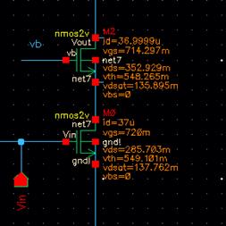
Figure 3. MOS transistors parameters.
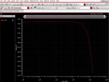
Figure 4. common-source stage gain.
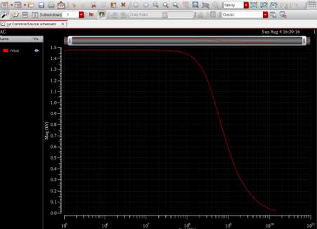
Figure 5. Cascode gain.
3.2. Folded cascode amplifier simulation
Subsequently, the research constructed a circuit structure for a folded cascode amplifier and performed preliminary simulations of its gain. The analysis included the utility of the differential pair input structure and examined the variations in circuit gain and output impedance with changes in circuit parameters, such as the width-to-length ratio. SPICE simulation software was used to simulate the gain of the folded common-source common-gate amplifier. The folded cascode circuit structure and the simulated circuit are shown in Figure 6 and 8, and the results of DC and AC analyses are depicted in Figure 7. The study utilized the pMOS_2V and nMOS_2V transistors from the TSMC18 process library for simulation. The research first set up the basic folded cascode amplifier circuit, including the establishment of the bias circuit, selection of appropriate supply voltage and load resistance. For the bias circuit, a constant current source with a current mirror structure was used to ensure stable current. Then the key transistor parameters, such as width-to-length ratio (W/L) and constant current source current, were set. Different parameter settings were used to simulate the circuit’s performance under various operating conditions [9].
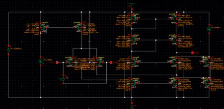
Figure 6. Folded cascode amplifier simulation circuit with mos transistors’ parameters.
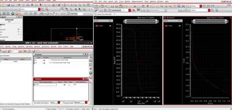
Figure 7. Circuit gain and Simulation parameters.
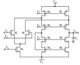
Figure 8. Input Folded cascode circuit structure.
4. Gain Optimization
The aforementioned content provides a fundamental study of the folded cascode amplifier. To enhance the gain of the common-source common-gate amplifier, optimization can be approached from several aspects. The following sections provide a detailed analysis.
Transconductance is a critical factor affecting the gain of a common-source amplifier. Enhancing transconductance can significantly increase the amplifier's gain. Raising the bias current can boost the transconductance. However, it is important to note that a higher bias current may lead to increased power consumption and potentially affect the circuit's thermal stability. Also, employing transistors with high transconductance properties, such as high-frequency field-effect transistors (HFETs) or metal-oxide-semiconductor field-effect transistors (MOSFETs), can effectively improve the amplifier's gain. Within the constraints of the fabrication process, many researchers select appropriate gate width and length ratios (W/L) to enhance the transconductance characteristics of the transistor. Some design a new structure to improve the gain [10].
In 2008, Zhang et al. proposed a method to effectively increase the gain of the folded cascode common-source common-gate amplifier. The study revealed that the parallel current sources introduced at the fold of the folded cascode structure reduced the small-signal impedance, thereby lowering the output resistance and significantly decreasing the gain. To address this issue, Zhang employed a current mirror structure in place of the traditional differential pair input method, which balanced the current distribution and thereby improved the small-signal gain. Additionally, research into frequency characteristics and power consumption showed that the practical impact of these factors was negligible, allowing the amplifier to potentially replace a two-stage operational amplifier in certain applications, thus enhancing economic efficiency [11].
In general, reducing the output resistance can also mitigate gain degradation. To reduce resistance, choosing transistors with inherently low output resistance, such as low-noise amplifier transistor, is an effective method. Moreover, introduce a resistor at the source of the common-source transistor to increase the equivalent output resistance, thereby reducing the impact of output resistance on gain. Implement constant current sources or current mirror circuits to provide a more stable bias current is also a efficient way to minimize the impact of current fluctuations on output resistance. Specifically, decoupling capacitors can be used in a stable bias circuit to filter out power supply noise and interference signals. As a result, bias voltage can maintain stable.
5. Frequency Characteristics Analysis
To gain a comprehensive understanding of the amplifier's performance, this study conducts a detailed analysis of its frequency response. Through simulation, the gain response curves of the common-source common-gate amplifier at various frequencies were obtained. The results indicate that the amplifier exhibits higher gain at lower frequencies, but the gain gradually decreases as the frequency increases. This reduction is primarily attributed to the effects of parasitic capacitance and inductance. At high frequencies, parasitic capacitance and inductance significantly impact the amplifier's performance. The parasitic capacitance includes the gate-source capacitance and gate-drain capacitance of the transistor. These capacitances create high-frequency paths that lead to a decrease in gain. Parasitic inductance, originating from circuit wiring and packaging, produces significant voltage drops at higher frequencies, further reducing the amplifier's gain.
Thus, it is significant to enhance the high-frequency performance of a common-source common-gate amplifier. First of all, optimizing circuit layout and selecting components with low parasitic capacitance between the gate and drain can reduce the impact of parasitic capacitance and improve high-frequency gain, which is most common way. Another useful method is to improve circuit layout by minimizing signal path lengths and optimizing routing. It can reduce the effects of parasitic inductance, consequently enhancing high-frequency performance. Second, optimizing wiring and selecting appropriate packaging to reduce the impact of parasitic inductance is crucial. Using short and wide traces can effectively lower parasitic inductance.
6. Future Development of Common Source Common Gate Amplifier
The common-source common-gate amplifier plays a main role in analog circuit design, particularly in high-frequency and broadband applications. With the continuous advancement of semiconductor technology, the emergence of new materials and device structures offers greater potential for enhancing the performance of common-source common-gate amplifiers.
Firstly, novel semiconductor materials such as silicon carbide (SiC), gallium arsenide (GaAs), and gallium nitride (GaN) are expected to play a significant role in high-frequency amplifier design due to their superior electron mobility and higher cutoff frequency. The utilization of these materials can substantially enhance amplifier gain and bandwidth, thus providing a solid foundation for the realization of millimeter-wave and terahertz communication systems.
In 2024, Shi et al. conducted a study on enhanced GaN devices and gate driver chips, designing a driving chip scheme for high-reliability GaN power devices. From a process perspective, they analyzed the impact of GaN's physical properties on the circuit, identified design challenges, and proposed solutions. Utilizing a 0.8 μm GaN on SOI process, the team performed a comprehensive simulation and verification of the driver chip system using Cadence software. The study focused on the design and simulation verification of the output driver stage circuit, revealing its good noise immunity and minimal delay mismatch [12].
For another, the advancement in nanometer-scale device structures will continue to drive the miniaturization and enhancement of amplifiers. As device dimensions decrease, parasitic capacitance and inductance will further diminish, which will contribute to improved high-frequency performance of the amplifiers. Moreover, the emergence of three-dimensional integrated circuit technology will facilitate the integration of amplifiers with other functional modules, resulting in more compact and efficient systems.
At last, in terms of circuit design methodologies, the introduction of artificial intelligence and machine learning is set to significantly transform the amplifier design process. Through AI algorithms, designers can more swiftly identify optimal circuit parameter combinations to enhance amplifier performance. Moreover, machine learning techniques can be employed to predict circuit performance, thereby reducing the time and cost associated with simulations and experiments, and accelerating the development of new products.
7. Conclusion
Through simulation, the study extensively investigates the gain characteristics of the cascode amplifier and proposes several optimization methods. The primary conclusions are as follows: The gain of the common-source common-gate amplifier is predominantly determined by the transconductance of the common-source stage and the whole output resistance. Significant improvements in amplifier gain can be achieved by increasing gm, reducing ro, and refining the biasing circuit. High-frequency performance is an important factor affecting amplifier efficacy. Effective enhancement of high-frequency response can be accomplished by minimizing parasitic capacitance and inductance, optimizing circuit layout, and introducing better compensation circuits.
Authors Contribution
All the authors contributed equally and their names were listed in alphabetical order.
References
[1]. Dresher R P and Irazoqui P P 2007 A compact nanopower low output impedance CMOS operational amplifier for wireless intraocular pressure recordings ANNUAL INTERNATIONAL CONFERENCE OF THE IEEE ENGINEERING IN MEDICINE AND BIOLOGY SOCIETY vols 1–16
[2]. Garde M P Lopez-Martin A Algueta-Miguel J M Beloso-Legarra J and Ramirez-Angulo J 2021 Energy-Efficient Symmetrical Cascode OTA in a 130 nm CMOS Process 2021 XXXVI Conference on Design of Circuits and Integrated Systems (DCIS) Vila do Conde Portugal pp 1–5
[3]. Wang J 2023 An accurate design method for folded cascode operational amplifier Electronic Science and Technology 36(03)50–54+68
[4]. Elsayed N Makhsuci S and Sanduleanu M 2024 A 28GHz Switched-Cascode Class E Amplifier in 22nm CMOS FDSOI Technology IEEE Journal of Microwaves 4(2) pp 246–252
[5]. Razavi Behzad 2018 Design of Analog CMOS Integrated Circuits (Xian Jiaotong University Press) pp 42–75
[6]. Venishetty S R 2019 Modified recycling folded cascode OTA with enhancement in transconductance and output impedance Turkish Journal of Electrical Engineering and Computer Sciences 27(6) pp 4472–4485
[7]. Xu Y 2021 Design of high-gain CMOS folded cascode operational amplifier Electronic World 20 pp 135–137
[8]. He H 2009 Research and design of CMOS high performance operational amplifier Fudan University
[9]. Deng H 2024 Design of a high-performance CMOS two-stage operational amplifier China Integrated Circuit 33(07) pp 50–56
[10]. Zhang Ch 2020 A subthreshold active cascode compensation operational amplifier Modern Electronic Technology 43(06) pp 13–17
[11]. Zhang Y 2008 Gain enhancement method of folded cascode amplifier stage Microcomputer Information 23 pp 311–312
[12]. Shi J 2023 Research on high reliability GaN power device gate drive circuit technology University of Electronic Science and Technology of China
Cite this article
Jiang,Y.;Zhao,L. (2024). Research and optimization of the gain characteristics of cascode amplifiers. Applied and Computational Engineering,101,247-255.
Data availability
The datasets used and/or analyzed during the current study will be available from the authors upon reasonable request.
Disclaimer/Publisher's Note
The statements, opinions and data contained in all publications are solely those of the individual author(s) and contributor(s) and not of EWA Publishing and/or the editor(s). EWA Publishing and/or the editor(s) disclaim responsibility for any injury to people or property resulting from any ideas, methods, instructions or products referred to in the content.
About volume
Volume title: Proceedings of the 2nd International Conference on Machine Learning and Automation
© 2024 by the author(s). Licensee EWA Publishing, Oxford, UK. This article is an open access article distributed under the terms and
conditions of the Creative Commons Attribution (CC BY) license. Authors who
publish this series agree to the following terms:
1. Authors retain copyright and grant the series right of first publication with the work simultaneously licensed under a Creative Commons
Attribution License that allows others to share the work with an acknowledgment of the work's authorship and initial publication in this
series.
2. Authors are able to enter into separate, additional contractual arrangements for the non-exclusive distribution of the series's published
version of the work (e.g., post it to an institutional repository or publish it in a book), with an acknowledgment of its initial
publication in this series.
3. Authors are permitted and encouraged to post their work online (e.g., in institutional repositories or on their website) prior to and
during the submission process, as it can lead to productive exchanges, as well as earlier and greater citation of published work (See
Open access policy for details).
References
[1]. Dresher R P and Irazoqui P P 2007 A compact nanopower low output impedance CMOS operational amplifier for wireless intraocular pressure recordings ANNUAL INTERNATIONAL CONFERENCE OF THE IEEE ENGINEERING IN MEDICINE AND BIOLOGY SOCIETY vols 1–16
[2]. Garde M P Lopez-Martin A Algueta-Miguel J M Beloso-Legarra J and Ramirez-Angulo J 2021 Energy-Efficient Symmetrical Cascode OTA in a 130 nm CMOS Process 2021 XXXVI Conference on Design of Circuits and Integrated Systems (DCIS) Vila do Conde Portugal pp 1–5
[3]. Wang J 2023 An accurate design method for folded cascode operational amplifier Electronic Science and Technology 36(03)50–54+68
[4]. Elsayed N Makhsuci S and Sanduleanu M 2024 A 28GHz Switched-Cascode Class E Amplifier in 22nm CMOS FDSOI Technology IEEE Journal of Microwaves 4(2) pp 246–252
[5]. Razavi Behzad 2018 Design of Analog CMOS Integrated Circuits (Xian Jiaotong University Press) pp 42–75
[6]. Venishetty S R 2019 Modified recycling folded cascode OTA with enhancement in transconductance and output impedance Turkish Journal of Electrical Engineering and Computer Sciences 27(6) pp 4472–4485
[7]. Xu Y 2021 Design of high-gain CMOS folded cascode operational amplifier Electronic World 20 pp 135–137
[8]. He H 2009 Research and design of CMOS high performance operational amplifier Fudan University
[9]. Deng H 2024 Design of a high-performance CMOS two-stage operational amplifier China Integrated Circuit 33(07) pp 50–56
[10]. Zhang Ch 2020 A subthreshold active cascode compensation operational amplifier Modern Electronic Technology 43(06) pp 13–17
[11]. Zhang Y 2008 Gain enhancement method of folded cascode amplifier stage Microcomputer Information 23 pp 311–312
[12]. Shi J 2023 Research on high reliability GaN power device gate drive circuit technology University of Electronic Science and Technology of China