


1. Introduction
With the continuous increase in the demand for high-performance and low-power consumption of modern electronic devices, the design and optimization of integrated circuits have become increasingly crucial and complex. Against this backdrop, the three main secondary effects, as three major physical phenomena, play significant roles in the design of transistors and their related circuits. The body effect mainly involves the electron migration characteristics in the main region of the transistor. Especially as the device size shrinks, the body effect has a remarkable influence on the threshold voltage and transconductance characteristics of the transistor [1-3]. This effect not only determines the switching speed of the transistor but also obviously changes the power consumption and also the performance of the circuit. The channel modulation effect is mainly manifested when the transistor is in the saturated region, resulting in a nonlinear correlation between the current and the channel length. With the increase in circuit frequency and the decrease in power consumption, reducing the channel modulation effect becomes one of the key challenges in circuit design. Effectively managing this effect can improve the reliability and performance stability of the circuit [4].
On the other hand, the subthreshold conduction effect affects the energy efficiency ratio and power control ability of the transistor at low voltage. In modern mobile device and sensor technology, optimizing the design of the subthreshold region to maximize battery life and system efficiency has become critical [5].
The purpose of this report is to explore in depth the basic principles, influencing factors, application and optimization strategies of these three secondary effects in modern integrated circuit design. Through systematic literature review and case analysis, these key effects will be more fully understood and applied to address increasingly complex circuit design challenges.
2. Theoretical Model and Basic Formula
2.1. Body effect
In NFET, when the substrate voltage becomes smaller, more holes are attracted to the substrate electrode, making the depletion layer wider. The VTH is the function of the total charge of the depletion layer, so as the substrate voltage decreases, the VTH will rise, thus affecting the drain current[6].
Threshold voltage of the MOS transistor:
 (1)
(1)
This indicates that as the substrate voltage VBS increases, the VTH will increase non-linearly. In design, this means that if the source potential is not fixed (as in some analog circuits), the body effect's impact on device performance needs to be considered.
Drain current:
 (2)
(2)
When the input Vin remains the same, the increase of VTH results in the decrease of Vout, as shown in the figure1 below.
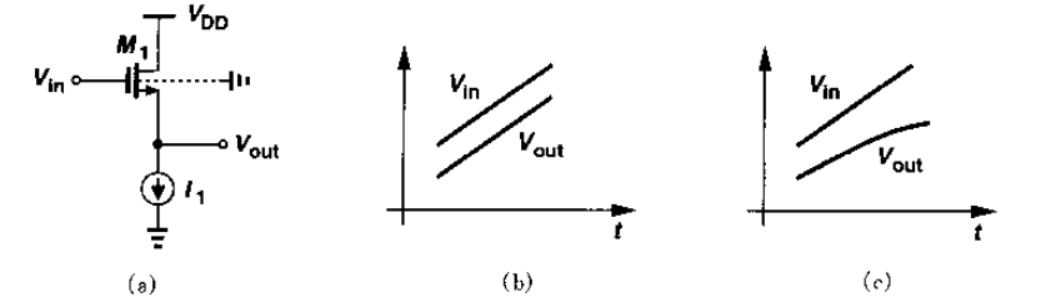
Figure 1. (a) Source-to-substrate voltage as a function of input level (b) Without considering the body effect (c) Considering the body effect[7].
The body effect can be eliminated as long as VSB=0 in the threshold voltage expression, which requires short connections between substrate and source. For example, when integrating, the PMOS monopolizes a trap, so that both the NMOS and the PMOS substrate can be connected to the source extremely short.
2.2. Channel length modulation effect
When the voltage difference between gate and drain increases, the actual inverse channel length gradually decreases. Channel modulation effect refers to the modulation effect of channel length change on drain current ID and transconductance gm.
Without considering the channel modulation effect:
 (3)
(3)
Figure 2 is the actual drain current change due to the channel modulation effect.
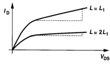
Figure 2. Drain current considering channel modulation effect [7].
The length of the actual channel:
 (4)
(4)
Drain current with channel modulation effect is considered:
 (5)
(5)
This shows that even in the saturation region, the drain current still increases with VDS. This means that the MOSFET's output resistance is finite, which in analog circuit design (such as amplifier) can affect the gain and frequency response of the circuit. The change of L also causes the change of transconductance gm.
Without considering the channel modulation effect:
 (6)
(6)
2.3. Subthreshold conduction effect
Under ideal circumstances, when the VGS< threshold voltage VTH, the MOS tube is cut off, and in fact, when it is less than the threshold, that is, when the threshold is lower, the MOS is also on and has a certain drain current ID, this phenomenon becomes a subthreshold conduction effect, which can be seen in figure3 [7].
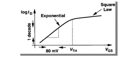
Figure 3. MOS subthreshold characteristics [7].
Subthreshold conduction phenomenon: The CMOS device can not be completely turned off when the VGS is very small, and there is leakage phenomenon, which will lead to power loss and analog (voltage or current) signal loss in the CMOS circuit. On the other hand, because the MOS tube is in the subthreshold region state, the power consumption can be lower than that after opening. Therefore, reasonable and correct use of sub-threshold conductivity of CMOS devices can achieve low voltage and low power design.
3. Practical Application of Secondary Effects
3.1. Examples of the application of body effects
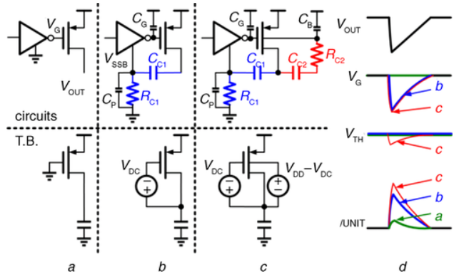
Figure 4. D-LDO connection and test bench (a) Conventional connection and test bench (b) AA connection and test bench (c) BD connection and test bench (d) Output waves of instantaneous output voltage (VOUT), gate voltage (VG), threshold voltage (VTH), and unit current (IUNIT) during a load step [8].
This figure 4 mainly shows the application and improvements of AA (Adaptive Automation) technology and BD (Partial Adaptive Automation) scheme in circuit design. Compared to traditional connection methods, AA technology enables a rapid response to load step changes without the need to increase sampling frequency or output capacitance. When combined with the BD scheme, the design can further optimize the threshold voltage, thereby enhancing the transient response capability while increasing the instantaneous value of the unit output current. By integrating the AA and BD schemes, the total coupling is reduced to 40 pF while still maintaining a good transient response. Compared to using the AA scheme alone, the performance improvement exceeds 10% [8].
3.2. DIBL effect compensation technique
The complementary metal oxide semiconductor voltage reference (CVR) has significant advantages in achieving low power consumption, which can be reduced to the nanowatt or petawatt level. The DIBL effect causes the ID of a subthreshold MOS transistor to depend on the VDS. In a self-biased or leak-biased CVR, the VDS of the bias transistor changes with the VDD, and the bias current will also change with the VDD due to the DIBL effect of the bias transistor, thus affecting the VREF.
In 2020, Wang et al. proposed a self-bias-based CVR structure, as shown in Figure 5, using a DIBL effect compensation technique. According to their design, by introducing an additional PMOS transistor M10, the current IC generated by its DIBL effect is VDD dependent, and the DIBL effect of the M6 transistor is successfully offset. This compensation technique makes the bias current IB independent of VDD, resulting in significantly improved load effects (LS). The CVR structure with this compensation technology has a load effect of only 0.019%/V and achieves a very low power consumption of only 48 pW [9].
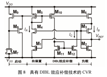
Figure 5. CVR with DIBL effect compensation technology[9].
Yu et al. also proposed a self-biased CVR structure with DIBL effect compensation in their study, as shown in Figure6. In order to reduce the dependence of IB caused by DIBL effect on supply voltage VDD, they designed the VGS1 of bias transistor M1 to adjust adaptively to achieve DIBL effect compensation. This design makes the bias current IB almost unaffected by VDD. According to their research, the circuit has an average load effect (LS) of 0.016%/V while achieving a lower power consumption of 521 Pw [10].
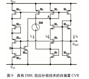
Figure 6. Self-biased CVR with DIBL effect compensation technology[10].
In practical circuit design, body effect and DIBL effect compensation have their own unique application scenarios and advantages. The main advantage of the bulk effect is its flexibility, suitable for applications where the threshold voltage needs to be dynamically adjusted, while the DIBL effect compensation is more suitable for circuit designs that require high stability. The combination of the two can achieve the best balance between performance and power consumption in complex circuit design, so as to meet the strict standards of modern integrated circuit design for high performance with low power consumption.
In addition to pre-regulation, self-regulation, and DIBL effect compensation techniques, increasing the output impedance of the bias transistor is another effective method for reducing source-drain voltage swing (LS). Yu et al. proposed an innovative approach by combining the standard current mirror (SCM) structure with a cascode configuration to create a quasi-self-cascode current mirror (QSCCM)[10]. This design increases output impedance, effectively reducing fluctuations in the bias current IB, thereby improving circuit stability and performance. This approach not only enhances operational efficiency but also offers new insights for the design of high-precision analog circuits.
4. Conclusion
With the continuous increase in the demand for high efficiency and low power consumption of modern electronic devices, the design and optimization of integrated circuits have become increasingly crucial and complex. Against this backdrop, these basic secondary effects, as three major physical phenomena, play significant roles in the design of transistors and their related circuits. The body effect mainly involves the electron migration characteristics in the main region of the transistor. Especially as the device size shrinks, the body effect has a remarkable influence on the threshold voltage and transconductance characteristics of the transistor. This effect not only determines the switching speed of the transistor but also directly affects the power consumption and overall performance of the circuit. The channel modulation effect is mainly manifested when the transistor is in the saturated region, resulting in a nonlinear correlation between the current and the channel length. With the increase of circuit frequency and the decrease of power consumption, reducing the channel modulation effect becomes one of the key challenges in circuit design. Effectively managing this effect can improve the reliability and performance stability of the circuit.
On the other hand, the subthreshold conduction effect affects the energy efficiency ratio and power control ability of the transistor at low voltage. In modern mobile device and sensor technology, optimizing the design of the subthreshold region to maximize battery life and system efficiency has become critical.
The purpose of this report is to explore in depth the basic principles, influencing factors, application and optimization strategies of three basic secondary effects in modern integrated circuit design. Through systematic literature review and case analysis, these key effects will be more fully understood and applied to address increasingly complex circuit design challenges.
References
[1]. Guo J Guo X Zhan G Ye C 2019 CMOS bandgap reference voltage source design based on subthreshold region Electron Prod World vol 31 no 02 pp 19-23
[2]. Li S Yu K Luo Z Su Z 2023 Research progress of ultra-low power CMOS voltage reference source technology Micro Nano Electron Intell Manuf vol 5 no 04 pp 6-12
[3]. Huang M Lu Y Lu X 2018 A partially analog assisted digital low-voltage differential regulator with transient body drive and 2.5× FOM improvement Electron Lett vol 54 pp 282-283
[4]. Huang C 2021 Research and application of MOSFET model based on surface potential Diss Univ Electron Sci Technol China
[5]. Chutham S Xiaolin Y Carolina M L 2023 Ultra-low-power voltage references exploring picowatt-level design using CMOS and hybrid architectures IEEE Solid-State Circuits Mag vol 15 no 4 pp 50-57
[6]. Seok M Sylvester D Blaauw D et al 2013 Reference voltage generator having a two transistor design US Patent
[7]. Bishop R 2018 Analog CMOS Integrated Circuit Design 2nd ed Xi'an Xi'an Jiaotong Univ Press pp 23-30
[8]. Chi X 2023 Research on temperature characteristics and modeling of FinFET devices Diss Univ Electron Sci Technol China
[9]. Wang Y Sun Q Luo H et al 2020 A 48 pW 0.34V 0.019%/V line sensitivity self-biased subthreshold voltage reference with DIBL effect compensation IEEE Trans Circuits Syst I Reg Papers vol 67 no 2 pp 611-621
[10]. Yu K Yang S Li S et al 2023 A 521pW 0.016%/V line sensitivity self-biased CMOS voltage reference with DIBL effect compensation using adaptive VGS control IEEE Trans Circuits Syst II Express Briefs
Cite this article
Ma,Y. (2024). The Application of Secondary Effects in Optimizing Analog Circuits. Applied and Computational Engineering,103,50-56.
Data availability
The datasets used and/or analyzed during the current study will be available from the authors upon reasonable request.
Disclaimer/Publisher's Note
The statements, opinions and data contained in all publications are solely those of the individual author(s) and contributor(s) and not of EWA Publishing and/or the editor(s). EWA Publishing and/or the editor(s) disclaim responsibility for any injury to people or property resulting from any ideas, methods, instructions or products referred to in the content.
About volume
Volume title: Proceedings of the 2nd International Conference on Machine Learning and Automation
© 2024 by the author(s). Licensee EWA Publishing, Oxford, UK. This article is an open access article distributed under the terms and
conditions of the Creative Commons Attribution (CC BY) license. Authors who
publish this series agree to the following terms:
1. Authors retain copyright and grant the series right of first publication with the work simultaneously licensed under a Creative Commons
Attribution License that allows others to share the work with an acknowledgment of the work's authorship and initial publication in this
series.
2. Authors are able to enter into separate, additional contractual arrangements for the non-exclusive distribution of the series's published
version of the work (e.g., post it to an institutional repository or publish it in a book), with an acknowledgment of its initial
publication in this series.
3. Authors are permitted and encouraged to post their work online (e.g., in institutional repositories or on their website) prior to and
during the submission process, as it can lead to productive exchanges, as well as earlier and greater citation of published work (See
Open access policy for details).
References
[1]. Guo J Guo X Zhan G Ye C 2019 CMOS bandgap reference voltage source design based on subthreshold region Electron Prod World vol 31 no 02 pp 19-23
[2]. Li S Yu K Luo Z Su Z 2023 Research progress of ultra-low power CMOS voltage reference source technology Micro Nano Electron Intell Manuf vol 5 no 04 pp 6-12
[3]. Huang M Lu Y Lu X 2018 A partially analog assisted digital low-voltage differential regulator with transient body drive and 2.5× FOM improvement Electron Lett vol 54 pp 282-283
[4]. Huang C 2021 Research and application of MOSFET model based on surface potential Diss Univ Electron Sci Technol China
[5]. Chutham S Xiaolin Y Carolina M L 2023 Ultra-low-power voltage references exploring picowatt-level design using CMOS and hybrid architectures IEEE Solid-State Circuits Mag vol 15 no 4 pp 50-57
[6]. Seok M Sylvester D Blaauw D et al 2013 Reference voltage generator having a two transistor design US Patent
[7]. Bishop R 2018 Analog CMOS Integrated Circuit Design 2nd ed Xi'an Xi'an Jiaotong Univ Press pp 23-30
[8]. Chi X 2023 Research on temperature characteristics and modeling of FinFET devices Diss Univ Electron Sci Technol China
[9]. Wang Y Sun Q Luo H et al 2020 A 48 pW 0.34V 0.019%/V line sensitivity self-biased subthreshold voltage reference with DIBL effect compensation IEEE Trans Circuits Syst I Reg Papers vol 67 no 2 pp 611-621
[10]. Yu K Yang S Li S et al 2023 A 521pW 0.016%/V line sensitivity self-biased CMOS voltage reference with DIBL effect compensation using adaptive VGS control IEEE Trans Circuits Syst II Express Briefs