


1. Introduction
With the development of modern electronics, the performance of the amplifier directly affects the overall effectiveness of the system. There has been a gradual shift in the design of operational amplifiers towards customised types. Design an amplifier with excellent performance while balancing all performance parameters. Amplifier gain can be increased by using a common-source, common-gate structure in the output stage, but the common-source, common-gate structure can severely limit the output voltage swing as the supply voltage decreases [1].
On the other hand, op-amp circuits are closely related to the degree of development of CMOS processes. From the familiar mp3, and mp4, to the present PDA, watch, and so on, these electronic products require very high speed and precision of the circuits [2]. As a result, the requirements for the devices are getting higher and higher. In turn, more circuit designs are produced that meet the requirements. In 2005, National Semiconductor Corporation successfully completed two high-speed, low-distortion, fully differential op-amps (LMH6550 and LMH6551) using a fully differential voltage feedback circuit design with a +5V or -5V supply voltage. The advantages are a bandwidth of up to 400 MHz and a spurious signal-free dynamic range of - 86 dBc [3]. as the process feature size decreases, the DC gain of the amplifier decreases dramatically, resulting in a serious degradation of the amplifier's performance [4]. In order to meet the overall system requirements, two-stage or multi-stage operational amplifiers have become a hot research topic.
In terms of integration, it ranges from small-scale (SSI) to medium-scale (MSI) and large-scale (LSI). Up to the current very large scale (VLSI) and ultra large-scale integrated circuits (ULSI). It can be seen that integrated circuits have undergone tremendous changes in recent decades [5].
This thesis presents a two-stage operational amplifier. A PMOS differential input, a typical common source stage structure, a PMOS self-bias circuit, and a Miller frequency compensation circuit are used to improve the performance of the operational amplifier. To simulate and analyse the two-stages operational amplifier circuit in cadence environment for each performance index and the parameters were optimised.
2. Fundamentals and Theory of Two-Stage Amplifier Design
2.1. Circuit structure and basic principle
In this design, the first stage amplifier is a differential amplifier, which can effectively reduce the effect of noise and reduce the input misalignment. The OTA five-tube structure is used, which is more suitable for IC integration by changing the bias current of the OTA, thus changing its interconductance gain gm and voltage amplifier gain Au [6]. The second stage amplifier is a common-source amplifier capable of providing a large gain with a large input impedance. For the design of the biasing circuit, a PMOS self-biasing circuit is chosen in this design, where the output current is weakly correlated with the power supply VCC. Finally, there is also a phase compensation circuit. Each additional amplification stage will generate at least one high impedance point. This in turn will introduce a pole, Excessive poles can greatly affect the stability of the amplifier [7]. The phase compensation circuit ensures the stability of the circuit.
2.2. Circuit analysis
2.2.1. Bias circuit. consisting of three pairs of current mirrors and keeping the left and right currents the same. Consistent aspect ratio for each pair of mos tubes. The magnitude of the current is related to M5M6 and R0. Because the VGS of the M5M6 is different, the VGS of the M5 will be smaller due to the presence of the resistor. So the shape aspect ratio needs to be adjusted to keep the currents on both sides similar. The voltage difference because of the difference in VGS and the magnitude of R0 determines the magnitude of the current. A bias voltage is supplied to the M14 gate along with the bias current, allowing the phase compensation circuit to operate in the proper interval. As shown in fig 1.
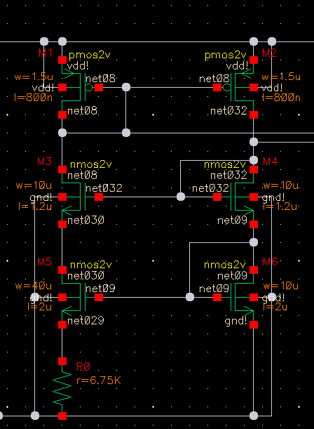
Figure 1. Bias circuit diagram
2.2.2. PMOS differential amplifier. M7M8 is used as a differential input pair, and the aspect ratio needs to be consistent to eliminate interference from noise and other factors. The M3M4 should have exactly the same aspect ratio as an NMOS current mirror load tube. M12 acts as a PMOS current mirror and as a tail current in the first stage of the amplifier circuit, providing a stable bias. Current mirror loaded structure means, the load of the differential amplifier is replaced by a current mirror[8]. Ensure that the circuit can work stably in the amplification region while reducing noise and distortion in the circuit. As shown in fig 2.
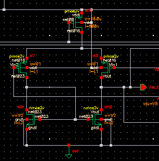
Figure 2. Differential circuit diagram
2.2.3. Common source level amplifier circuit and phase compensation circuit. M13 acts as a PMOS current mirror and acts as a load for the second stage amplifier, where the current changes through the load thus generating an output voltage signal. Make M14 operate in the linear region so that it is equivalent to a resistor. By adjusting the size of the resistor, the action of moving the zero point of the right half plane can be achieved. The mos tube is connected across the input and output of the second stage along with the capacitor C0 to form the RC Miller compensation. The role is to ensure a suitable phase margin. As shown in fig 3.
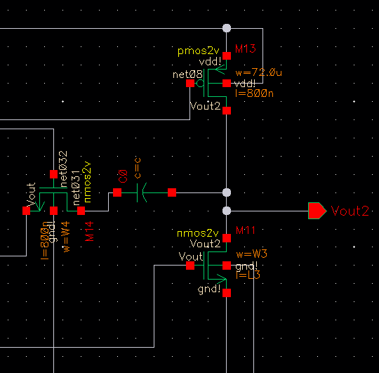
Figure 3. Common source level stage and phase compensation circuit diagrams
3. Analysis and Optimisation of Cadence Simulation Results
3.1. Circuit structure and basic principle
During the commissioning of the first stage, it is necessary to make the gain as large as possible while the mos is in the saturation region. Therefore, the choice was made to change the aspect ratio of the mos for debugging. Secondly, in order to match the primary and secondary amplifiers, it is required that VGST9=VGST10=VGST11, IDS9/(W/L)9=IDS10/(W/L)10=IDS11/(W/L)11. The amplification gain interval is obtained after satisfying the above conditions. As shown in fig4. The red line is the primary gain = 100 and the total circuit gain = 1.3k.
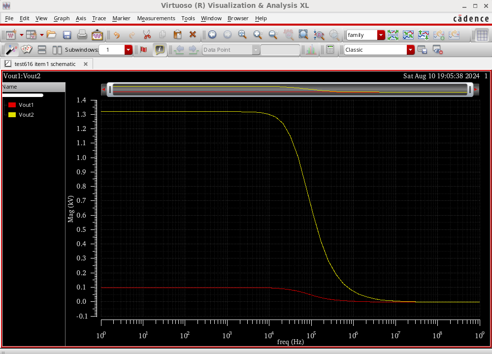
Figure 4. Circuit gain diagram
In phase compensation circuits, C0 enlargement enhances the pole-splitting function, reduces the input integration noise, reduces the second stage power consumption, and improves the phase margin. However, the disadvantage is that it reduces the GBW and the slew rate. The preset C0 is thus changed to 1.2 pf. Next, make sure that the NMOS is in the linear region. The phase margin and op-amp gain bandwidth are shown in fig5. From the red line, the GBW of the op-amp is 67 MHZ with a phase margin of 70°.
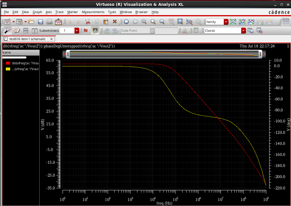
Figure 5. Gain bandwidth and phase margin chart
3.2. Circuit structure and basic principle
By introducing unit gain negative feedback in the secondary amplification region, as shown in fig 6. Connect the output to the negative terminal of the input, at which point Vout is no longer determined by the parameters of the load and amplifier tubes.Because the DC gains of the secondary op-amps are all high enough, Vin+ approximates Vin-. In summary, Vout is directly determined by the DC voltage of Vin+. Under the premise of negative feedback, the op-amp can automatically adjust the Vgs of the amplifier so that the amplifier current is constantly equal to the saturation current of the load tube. Thus the boundary condition that guarantees simultaneous saturation of the load and amplifier tubes becomes a range.
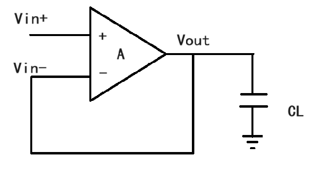
Figure 6. Unit gain negative feedback circuit diagram
In terms of power consumption, in 2018, the Belgian Microelectronics Research Centre launched 3nm chips, and lower-size chips are also under research, so the design of semiconductor integrated circuits with low voltage and low power consumption has become one of the research hotspots in the center of the international research institutes [9]. Many new compensation methods have been proposed for phase compensation. Damping Factor Controlled Frequency Compensation (DFCFC) greatly improves the GBW by adding a damping network. However, DFCFC is suitable for large load capacitance. For smaller load capacitances, DFCFC does not show good characteristics [10].
4. Conclusion
The present design of the two-stage amplifier achieves a large gain multiplier over a large frequency range by combining different characteristic amplifier circuits and adjusting the component parameters. Future developments for two-stage or multi-stage operational amplifier circuits aim to improve the circuit or introduce negative feedback to improve the performance of the circuit. It can be seen that the performance of operational amplification circuits in the enhancement of diversification, can be customised through the specific needs of targeted amplification circuits, with the improvement of the overall performance of the equipment, which is also a popular direction for the future development of operational amplification circuits. On the other hand, while cascading different amplifiers, studying negative feedback circuits is also one of the research hotspots. Introducing high-performance negative feedback can effectively enhance the stability of the circuit.Ensure stable amplification under external environmental interference.
References
[1]. Qin C Zhang L Zhou C et al 2017 Dual AC Boosting Compensation Scheme for Multistage Amplifiers IEEE Transactions on Circuits and Systems-II 64(8) pp 882-886
[2]. Li S 2015 Research and Design of CMOS Fully Differential Amplifier Heilongjiang University pp 1-75
[3]. Rodanas Valero M Celma S Medrano N 2012 An Ultra Low-Power Low-Voltage Class-AB Fully Differential Opamp for Long-Life Autonomous Portable Equipment IEEE (10) pp 643-647
[4]. Watkins G Mimi K 2016 A Dynamic Load Modulation RF Amplifier with Current Mirror Based Varactor Diver Amplifier Act & Pass RF Dev Seminar 2(6) pp 1-4
[5]. Chen H Milovanović V Giotta D 2013 Ultra-High Bandwidth Fully-Differential Three-Stage Operational Amplifiers in 40nm Digital CMOS IEEE (13) pp 76-81
[6]. Tian J Wang S Lai X et al 2006 A Novel Digital-to-Analogue Converter with OTA Structure Electronic Science and Technology (3) pp 4 DOI10.3969/jissn1007-7820200603004
[7]. He Y Xiao Z Wang Y et al 2020 Design of a High-Efficiency ACBC-C Three-Stage Op-Amp Electronic Technology Applications 46(06) pp 36-39+50
[8]. Tang Y Wan P Guo L 2012 Analysis of Common Mode Stability in Fully Differential Operational Amplifiers China Integrated Circuits (5) pp 22-25
[9]. Nagy L Arbet D Kovac M et al 2018 Design and Performance Analysis of Ultra-Low Voltage Rail-to-Rail Comparator in 130 nm CMOS Technology 2018 IEEE 21st International Symposium on Design and Diagnostics of Electronic Circuits & Systems (DDECS) IEEE pp 51-54
[10]. Ribner D B Copeland M A 1984 Design Techniques for Cascoded CMOS Op Amps with Improved PSRR and Common-Mode Input Range IEEE Journal of Solid-State Circuits 19(6) pp 919-925
Cite this article
Chen,Z. (2024). Design and optimisation of a two-stage amplifier based on a differential input stage and a common-source amplifier. Applied and Computational Engineering,104,104-109.
Data availability
The datasets used and/or analyzed during the current study will be available from the authors upon reasonable request.
Disclaimer/Publisher's Note
The statements, opinions and data contained in all publications are solely those of the individual author(s) and contributor(s) and not of EWA Publishing and/or the editor(s). EWA Publishing and/or the editor(s) disclaim responsibility for any injury to people or property resulting from any ideas, methods, instructions or products referred to in the content.
About volume
Volume title: Proceedings of the 2nd International Conference on Machine Learning and Automation
© 2024 by the author(s). Licensee EWA Publishing, Oxford, UK. This article is an open access article distributed under the terms and
conditions of the Creative Commons Attribution (CC BY) license. Authors who
publish this series agree to the following terms:
1. Authors retain copyright and grant the series right of first publication with the work simultaneously licensed under a Creative Commons
Attribution License that allows others to share the work with an acknowledgment of the work's authorship and initial publication in this
series.
2. Authors are able to enter into separate, additional contractual arrangements for the non-exclusive distribution of the series's published
version of the work (e.g., post it to an institutional repository or publish it in a book), with an acknowledgment of its initial
publication in this series.
3. Authors are permitted and encouraged to post their work online (e.g., in institutional repositories or on their website) prior to and
during the submission process, as it can lead to productive exchanges, as well as earlier and greater citation of published work (See
Open access policy for details).
References
[1]. Qin C Zhang L Zhou C et al 2017 Dual AC Boosting Compensation Scheme for Multistage Amplifiers IEEE Transactions on Circuits and Systems-II 64(8) pp 882-886
[2]. Li S 2015 Research and Design of CMOS Fully Differential Amplifier Heilongjiang University pp 1-75
[3]. Rodanas Valero M Celma S Medrano N 2012 An Ultra Low-Power Low-Voltage Class-AB Fully Differential Opamp for Long-Life Autonomous Portable Equipment IEEE (10) pp 643-647
[4]. Watkins G Mimi K 2016 A Dynamic Load Modulation RF Amplifier with Current Mirror Based Varactor Diver Amplifier Act & Pass RF Dev Seminar 2(6) pp 1-4
[5]. Chen H Milovanović V Giotta D 2013 Ultra-High Bandwidth Fully-Differential Three-Stage Operational Amplifiers in 40nm Digital CMOS IEEE (13) pp 76-81
[6]. Tian J Wang S Lai X et al 2006 A Novel Digital-to-Analogue Converter with OTA Structure Electronic Science and Technology (3) pp 4 DOI10.3969/jissn1007-7820200603004
[7]. He Y Xiao Z Wang Y et al 2020 Design of a High-Efficiency ACBC-C Three-Stage Op-Amp Electronic Technology Applications 46(06) pp 36-39+50
[8]. Tang Y Wan P Guo L 2012 Analysis of Common Mode Stability in Fully Differential Operational Amplifiers China Integrated Circuits (5) pp 22-25
[9]. Nagy L Arbet D Kovac M et al 2018 Design and Performance Analysis of Ultra-Low Voltage Rail-to-Rail Comparator in 130 nm CMOS Technology 2018 IEEE 21st International Symposium on Design and Diagnostics of Electronic Circuits & Systems (DDECS) IEEE pp 51-54
[10]. Ribner D B Copeland M A 1984 Design Techniques for Cascoded CMOS Op Amps with Improved PSRR and Common-Mode Input Range IEEE Journal of Solid-State Circuits 19(6) pp 919-925