


1. Introduction
The integrated circuit industry has been continuously developing and advancing over time. Integrated circuits are now classified by their scale, including small, medium, large, and very-large-scale integration (VLSI). With continuous advancements in technology, improvements in the capacity and speed of integrated circuits have also become evident.
There is a well-known principle in integrated circuits called Moore's Law. This law states that approximately every two years, the number of transistors that can be accommodated on an integrated circuit will double, resulting in a corresponding increase in computing power. This principle suggests that as technology progresses, computer performance will grow exponentially, while costs will relatively decrease. Moore's Law reflects both the pattern of development in the electronics and information industry and the pace of technological innovation.
Although in recent years, growth in the size of integrated circuits has slowed due to bottlenecks in foundational areas such as semiconductor physics and device technology, integrated circuits have not yet reached the limit of their feature sizes. The growth rate still allows for doubling every two to three years. Currently, most chips use low-power complementary metal-oxide-semiconductor (CMOS) structures [1]. However, due to the increased integration, transistor count, and operating frequency, the overall power consumption of chips remains high.
In summary, during the early stages of integrated circuit development, power consumption was not a prominent issue due to the relatively small scale of circuits. The main focus was on chip speed and area, while power consumption was a relatively secondary consideration [2]. However, with the rapid growth of the chip industry, attention to power consumption in chip design has significantly increased. Both academic and industrial sectors, domestically and internationally, are heavily invested in the research and application of low-power design. Some large chip companies have even established dedicated teams focused on low-power chip design, further underscoring the critical importance of power management.
2. Sources of Power Consumption in CMOS Integrated Circuits
In today's highly integrated chips, CMOS devices are widely used due to their numerous advantages, such as low power consumption, strong anti-interference capability, wide power supply voltage range, high input impedance, strong load-driving capability, and large logic swings. Among them, power consumption is primarily composed of dynamic and static elements. Dynamic energy refers to the power consumed during the switching of gate outputs during logic transitions, and it primarily consists of short-circuit power (conduction power) and switching power. Static power, on the other hand, is mainly caused by leakage current and is also referred to as leakage power [3]. Therefore, the total power consumption can be expressed as shown in Equation (1), with the main sources of total power being short-circuit current power, switching power, and leakage power.
\( {P_{total}}={P_{switch}}+{P_{internal}}+{P_{leakage}} \) (1)
2.1. Switching Power (P_switch)
When the input signal switches states, the load capacitanceCL charges and discharges at the output in response to the signal transition, resulting in power consumption.
|
Figure 1: Charging and Discharging Diagram of a Simple CMOS Inverter Circuit. |
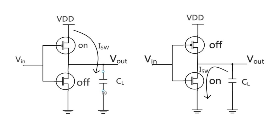
As shown in Figure 1, when Vin is at a low level, the PMOS transistor conducts, whereas the NMOS transistor remains inactive, causing Vout to be at a high level. At this point, the output charges the load capacitance CL. When Vin is at a high level, the PMOS transistor remains inactive, while the NMOS transistor is activated, causing Vout to be at a low level. Since the load capacitance CL was charged when Vin was at a low level, it will discharge when Vout is at a low level.
From the perspective of power consumption, when the inverter undergoes a transition from a low potential to a high potential, the load capacitance CL draws \( {C_{L}}V_{DD}^{2} \) joules of energy supplied by VDD. This energy will be retained in the capacitor and dissipated in the transistor in the form of heat. When the input transitions from a high state to a low stat, the energy stored in the capacitor is dissipated through the NMOS transistor during discharge [4]. Short-circuit current power consumption (P_internal) and switching power consumption increase during the charging and discharging process. Therefore, the calculation of dynamic power must also consider the switching probability, as expressed in the following equation.
\( {P_{switch}}=α∙V_{DD}^{2}∙{C_{L}}{∙f_{clk}} \) (2)
VDD represents the power supply voltage, α is the switching factor, defined as the likelihood of signal transitions caused by clock transitions, and \( f \) clk is the clock frequency. Switching power constitutes the major portion of the energy consumption in CMOS circuits. From the equation, it can be concluded that switching power can be controlled by reducing VDD , the switching probability, load capacitance, and operating frequency.
2.2. Short-Circuit Power (P_internal)
In an ideal situation, the input signal of an inverter is a step signal, so at the same time point, only one of the P or N transistors is on while the other is off. This means there is no direct current pathway between the power supply and ground, which leads to zero power loss [5]. However, in actual circuits, due to signal delay, N and P transistors may turn on simultaneously at certain times, leading to the appearance of short-circuit current and causing short-circuit power consumption. To minimize this power consumption as much as possible, the rise or fall time of the output can be limited to be greater than the input transition time in order to optimize short-circuit current. However, this results in a longer output transition time, which lowers circuit speed, impacts the short-circuit power consumption of the next stage, and may cause transition time violations or even timing issues. Therefore, when optimizing short-circuit current power consumption, both local and global effects should be considered comprehensively [6]. The relationship is expressed as follows:
\( {P_{internal}}=VDD∙T∙{I_{short}}{∙f_{clk}} \) (3)
In the above equation, VDD represents the power supply voltage, T is the short-circuit time during which both the N and P transistors are turned on at the same time, Ishort is the short-circuit current, and \( f \) clk is the clock frequency. It can be concluded that short-circuit power consumption is directly proportional to the power supply voltage, short-circuit time, short-circuit current, and clock frequency.
2.3. Static Power Loss
Static power consumption mainly comes from the leakage power of transistors. In ideal circumstances, a direct current path between the power supply and ground would not exist, resulting in no static power consumption. However, in real circuits, there is always some leakage current. While this current is small enough to be negligible for a single transistor, as the number of transistors in modern chips increases due to technological advancements, static power consumption also intensifies due to the growing number of transistors. Leakage current primarily originates from:
• Subthreshold current: When the transistor operates in the subthreshold region, although the gate voltage is below the threshold voltage, a small amount of current will still flow.
• Gate leakage current: When there is a voltage at the gate, a current will be generated due to the electric field between the gate and the substrate, causing electrons to flow from the substrate to the gate or from the gate to the substrate.
• Reverse-biased junction current: There can be leakage current through the PN junction that is reverse-biased between the source or drain and the substrate [7].
3. Low-Power Design
3.1. System Architecture-Level Low-Power Design
3.1.1. System Architecture-Level Low-Power Design.
From the previous power consumption equation, it can be understood that voltage is closely related to power consumption. The multi-voltage design approach includes:
(a) Different voltage regions have their own fixed voltage.
(b) Different voltage regions have their own fixed voltage, and software determines which voltage region to select.
(c) An adaptive approach is used, where the voltage regions are variable, and the software decides which voltage region to select
3.1.2. System Architecture-Level Low-Power Design
In the design process, system functions can be implemented using either hardware or software, though the majority of the system's power consumption is attributed to the hardware units. During this process, the way the software organizes and interacts with the hardware has a significant effect on power consumption. Therefore, in the design process, while meeting usage requirements, the voltage should be kept as low as possible, and timing requirements must also be satisfied. This requires selecting which parts of the system to implement in hardware or software based on the required performance.
3.1.3. System Clock Design
The clock is the highest frequency signal in the system, and power consumption also increases significantly during the continuous toggling of the clock. Therefore, during the design phase, the clock module should be controlled according to the specific requirements of different applications. Different clock frequencies should be selected for different modes, and unused clocks should be turned off in certain states.
3.2. RTL-Level Low-Power Design
At the RTL stage, the primary emphasis is on minimizing switching activity in the design. Since switching activity is proportional to dynamic power consumption, reducing it can effectively lower dynamic power. Switching activity is determined by the transition probability and the number of transitions per unit time. Therefore, power reduction can be approached by minimizing these two factors. During RTL coding, it is important to reduce unnecessary transitions as much as possible. Since signal transitions cause circuit switching, one way to reduce switching activity is by using a one-hot encoding scheme to decrease the number of bits that switch. For example, in a sequence like 0000, 0001, 0010, 0100, regardless of how the state transition occurs, only 2 bits change between adjacent states. This approach helps mitigate the uncertainties caused by speed and race conditions in the circuit.
Circuit switching is also caused by the presence of glitches. Glitches are the result of race conditions and hazards in the circuit. Due to the differences in delays and paths in various parts of the circuit, the arrival times of signals at a node may vary, which leads to the generation of glitches at the output.
3.3. Clock Gating Technology
Power usage in CMOS circuits is closely related to frequency. Typically, the clock tree consists of numerous buffers and inverters, and in program design, the clock signal is often kept toggling continuously. As a result, clock power consumption accounts for at least 30% of the chip’s dynamic power consumption [8]. Power can be reduced by masking and minimizing signal transitions to prevent unnecessary signal propagation to subsequent stages. The primary methods include reducing the capacitive load of the clock network, lowering the power consumption of internal registers, and minimizing the number of required multiplexers.
|
Figure 2: Clock Gating Circuit Diagram. |
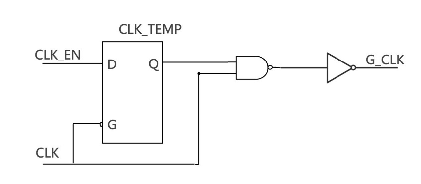
As illustrated in Figure 2, when the clock signal (CLK) is low, the latch is transparent (connected); when CLK is high, the latch holds its state (locked). This means that when CLK is low, G_CLK is also low. However, when CLK is high, the value of G_CLK reflects the value of EN at the rising edge of CLK. Thus, the latch can effectively retain the value of EN without impacting the CLK cycle. Additionally, clock gating technology can facilitate low-power memory design by efficiently trimming the clock tree [9].
3.4. Multi-Threshold Voltage Technology
With the continuous advancement of semiconductor technology, the size of semiconductor devices has been shrinking, and the number of transistors within devices has increased. As a result, supply voltages have decreased, and threshold voltages have also become lower. Therefore, power consumption must be optimized accordingly during design. Since threshold voltage has an exponential impact on leakage power, cells with a higher threshold voltage exhibit reduced leakage power but slower speed, whereas cells with a lower threshold voltage experience increased leakage power but faster speed. In our design, we can take advantage of the characteristics of a multi-threshold voltage library to create high-performance designs. For example, in a design with multiple timing paths, the path with the longest delay is called the critical path. To meet timing requirements, low-threshold voltage cells may be applied along the critical path to reduce delay and improve timing. On non-critical paths, high-threshold voltage cells can be employed to lower static power consumption. Therefore, the appropriate use of different multi-threshold cells can enable the design of chips with reduced static leakage power and high performance[10].
3.5. Power Gating Technology
At the current level of technology, even if the circuit is not switching, it still consumes a significant amount of static power. This necessitates the use of power gating technology. The main idea is that when a certain module is inactive for a period of time, its power supply can be turned off, and when needed, it can be turned back on. To quickly resume operation, the state of the module is preserved before the power is turned off.
The first part of this work explores the sources of power consumption, revealing that power consumption in circuits mainly comes from static and dynamic power. The equations are analyzed to investigate the factors influencing these two types of power consumption. Based on these influencing factors, the later part discusses several low-power design techniques.
4. Conclusion
With the continuous improvement in integrated circuit manufacturing processes and the increasing demand for low power consumption and high reliability, significant advancements have been made in low-power design technologies for integrated circuits, while also placing greater emphasis on research in low-power technologies.
The main work of this paper includes a detailed analysis of the sources of power consumption in CMOS circuits, which primarily come from the static and dynamic power of transistors. From the perspective of equations, both categories were analyzed, revealing the basic directions and methods for reducing power consumption. These include approaches related to supply voltage, clock frequency, load capacitance, switching activity, and leakage current. Various low-power techniques for integrated circuits were also analyzed, including system architecture-level low-power design, RTL-level low-power design, clock gating, multi-threshold voltage technology, and power gating.
Due to my limited knowledge and capabilities, I have only explored a few aspects of low-power design in this work. Firstly, the methods applied in this paper represent just a fraction of the available low-power design techniques, and there are many other methods that I have yet to explore. Additionally, in terms of power analysis, I hope that in future research, I can leverage more advanced tools and methods, such as performing more detailed power evaluations through the measurement of actual chips in combination with back-end simulation tools, rather than being limited to estimations in the front-end and mid-stage design phases.
References
[1]. Pelgrom M.J.M.;Aad L..Matching Properties Of MOS Transistors[J].IEEE Journal of Solid-State Circuits,1989(5)
[2]. Massoud Pedram.Power minimization in IC design[J].ACM Transactions on Design Automation of Electronic Systems (TODAES),1996(1).
[3]. L. C, C. T. K, N. Pinto, V. P. B. R, S. Shankar and R. K. R, "Advanced CMOS VLSI Technology for Low Power Analog System Design with High Gain," 2022 IEEE International Conference on Distributed Computing and Electrical Circuits and Electronics (ICDCECE), Ballari, India, 2022, pp. 1-6, doi: 10.1109/ICDCECE53908.2022.9793203.
[4]. Yu Mei. Research on Low-Power Design Methods for SOC [D]. Fudan University, 2008..
[5]. Zhang Zhengkai. Research on Low-Power Design Methods for Digital Chips [D]. University of Electronic Science and Technology of China, 2008.
[6]. Binglong Zhang;Balasinski A..Hot-carrier effects on gate-induced-drain-leakage (GIDL) current in thin-film SOI/NMOSFET's[J].IEEE Electron Device Letters,1994(5).
[7]. Zhang Yu. Design and Verification of Low-Power Timer Based on MCU [D]. Xidian University, 2008.
[8]. V.G. Oklobdzija, "Digital System Clocking-High-Performance and Low-Power Aspects" in , New York, NY, USA:Wiley, 2003.
[9]. G. S. R. Srivatsava, P. Singh, S. Gaggar and S. K. Vishvakarma, "Dynamic power reduction through clock gating technique for low power memory applications," 2015 IEEE International Conference on Electrical, Computer and Communication Technologies (ICECCT), Coimbatore, India, 2015, pp. 1-6, doi: 10.1109/ICECCT.2015.7226204.
[10]. Yu Xiqing, ed. Practical Guide to Application-Specific Integrated Circuit Design [M]. Zhejiang University Press, 2007.
Cite this article
Wang,S. (2025). Research on Low-Power Design Methods for Integrated Circuits. Applied and Computational Engineering,128,18-23.
Data availability
The datasets used and/or analyzed during the current study will be available from the authors upon reasonable request.
Disclaimer/Publisher's Note
The statements, opinions and data contained in all publications are solely those of the individual author(s) and contributor(s) and not of EWA Publishing and/or the editor(s). EWA Publishing and/or the editor(s) disclaim responsibility for any injury to people or property resulting from any ideas, methods, instructions or products referred to in the content.
About volume
Volume title: Proceedings of the 5th International Conference on Materials Chemistry and Environmental Engineering
© 2024 by the author(s). Licensee EWA Publishing, Oxford, UK. This article is an open access article distributed under the terms and
conditions of the Creative Commons Attribution (CC BY) license. Authors who
publish this series agree to the following terms:
1. Authors retain copyright and grant the series right of first publication with the work simultaneously licensed under a Creative Commons
Attribution License that allows others to share the work with an acknowledgment of the work's authorship and initial publication in this
series.
2. Authors are able to enter into separate, additional contractual arrangements for the non-exclusive distribution of the series's published
version of the work (e.g., post it to an institutional repository or publish it in a book), with an acknowledgment of its initial
publication in this series.
3. Authors are permitted and encouraged to post their work online (e.g., in institutional repositories or on their website) prior to and
during the submission process, as it can lead to productive exchanges, as well as earlier and greater citation of published work (See
Open access policy for details).
References
[1]. Pelgrom M.J.M.;Aad L..Matching Properties Of MOS Transistors[J].IEEE Journal of Solid-State Circuits,1989(5)
[2]. Massoud Pedram.Power minimization in IC design[J].ACM Transactions on Design Automation of Electronic Systems (TODAES),1996(1).
[3]. L. C, C. T. K, N. Pinto, V. P. B. R, S. Shankar and R. K. R, "Advanced CMOS VLSI Technology for Low Power Analog System Design with High Gain," 2022 IEEE International Conference on Distributed Computing and Electrical Circuits and Electronics (ICDCECE), Ballari, India, 2022, pp. 1-6, doi: 10.1109/ICDCECE53908.2022.9793203.
[4]. Yu Mei. Research on Low-Power Design Methods for SOC [D]. Fudan University, 2008..
[5]. Zhang Zhengkai. Research on Low-Power Design Methods for Digital Chips [D]. University of Electronic Science and Technology of China, 2008.
[6]. Binglong Zhang;Balasinski A..Hot-carrier effects on gate-induced-drain-leakage (GIDL) current in thin-film SOI/NMOSFET's[J].IEEE Electron Device Letters,1994(5).
[7]. Zhang Yu. Design and Verification of Low-Power Timer Based on MCU [D]. Xidian University, 2008.
[8]. V.G. Oklobdzija, "Digital System Clocking-High-Performance and Low-Power Aspects" in , New York, NY, USA:Wiley, 2003.
[9]. G. S. R. Srivatsava, P. Singh, S. Gaggar and S. K. Vishvakarma, "Dynamic power reduction through clock gating technique for low power memory applications," 2015 IEEE International Conference on Electrical, Computer and Communication Technologies (ICECCT), Coimbatore, India, 2015, pp. 1-6, doi: 10.1109/ICECCT.2015.7226204.
[10]. Yu Xiqing, ed. Practical Guide to Application-Specific Integrated Circuit Design [M]. Zhejiang University Press, 2007.