


1. Introduction
Currently, given the rapid pace that digitization and informatization are developing, the development and application of digital integrated circuits are very important. Digital integrated circuits are developing in the direction of higher integration and faster speed. So far, the development of integrated circuits has continued to follow Moore's Law, where the level of integration doubles roughly every 18 months. At the same time, as digital circuits develop in the direction of high integration and high speed, the power consumption of the circuits also increases, and power consumption optimization is an essential part of the design process of digital integrated circuits [1]. This is because a rise in power consumption means an increase in electron mobility, which will lead to an increase in the temperature of the circuit or chip. If the temperature rises to a particular level, the reliability in the whole system will be impacted [1]. Electronics require batteries to power. The dimensions and mass of the battery are closely related to the capacity of the battery. Currently, many electronic products are moving towards high reliability and portability, so the optimization of power consumption in digital integrated circuits is very critical. At the same time, excessive power consumption has a certain degree of impact on the stability of digital integrated circuits since low-power design is becoming a trend in this field [2]. Digital comparators have a wide range of applications in digital integrated circuits. For example, A/D conversion is the process of converting analog signals into digital signals. First, the analog signal is measured to determine its digital amount. Next, the analog signal and reference signal are evaluated, and the binary signal is output based on the comparison results of the comparator [3]. Since the comparison speed and power consumption of the comparator play a crucial part in the processing speed as well as the energy consumption of the A/D conversion, it is crucial to optimize the speed and energy consumption of the comparator [3]. More sophisticated molecular logic gates that can carry out several sensing tasks at once have been created as a result of the quick advancements in fluorescence probes and fluorescent sensing materials. [4]. As technology and science have advanced, the construction of comparators at the molecular level has become a reality [4]. Because the design of digital comparators is easier to expand to higher order bits, they are widely used in the VLSI field [5]. Since digital comparators are frequently involved in digital integrated circuits, an in-depth study of low-power and high-speed digital comparators is of great significance.
This paper designs a digital comparator, the digital comparator designed in this paper can compare two sets of three-bit values. Based on the implementation of the digital comparison function, the digital comparator is optimized for energy consumption. The energy consumption at 1V supply voltage is analyzed and the comparator designed in this paper is optimized from a certain angle of reducing the supply voltage.
This paper analyzes the development and application trends of digital integrated circuits and the wide application of digital comparators in digital circuits. The current digital integrated circuit design is developing in the direction of low power design, while digital comparators play an important role in digital integrated circuits. Thus, in this paper, a digital comparator is designed and analyzed from the angle of reducing the supply voltage, reducing the energy consumption of the comparator and thus optimizing the digital comparator. Meanwhile, the function of the digital comparator designed in this paper is simulated by Multisim software and the comparator is able to realize the corresponding function. In future research, different perspectives will be tried to optimize the energy consumption of the comparator, not just from the perspective of reducing the supply voltage, but also from the angle of the logic gate level.
2. Circuit design
The digital comparator designed in this paper consists of CMOS gate circuits, which include three fundamental kinds of logic gates consisting of NOT gate, NOR gate, NAND gate, which allow the signal to pass when the desired condition is met [6].
Since the NMOS inverter output low level is not ‘0’ and has high energy loss, CMOS inverter is used in this design [7]. The principle of NOT gate is composed of two complementary MOSFET (NMOS and PMOS), the gate of the two transistors is connected to the incoming signal, the drain is connected as the output, the NMOS source is grounded and the PMOS source is connected to the operating voltage [8]. When the input signal is high, the PMOS cuts off, the NMOS conducts, the output logic pulls down, and the outcome signal is ‘0’. In the event that the information entered is low, the PMOS conducts, the NMOS cuts off, and the logic value from the outcoming port pulls high. The function of the NOT gate is to invert the provided data to get the result signal, which is logically opposite to the incoming signal. Figure 1 shows the schematic diagram of NOT gate and Table 1 shows the truth table of NOT gate, A represents the input data and Y represents the result of the output.
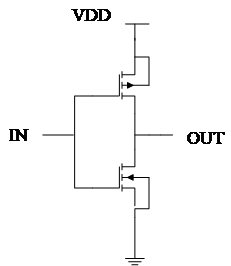
Figure 1: Schematic diagram of NOT gate.
Table 1: NOT gate truth table.
A | Y |
0 | 1 |
1 | 0 |
The principle of NOR gate is that when the input signals are both low, the parallel switch cuts off, the series switch conducts, and the result logic is pulled high. When all input information is ‘0’, the result from the port of output is ‘1’, otherwise the entered data is ‘0’. Figure 2 shows the schematic diagram of the NOR gate and table 2 shows the truth table of NOR gate, where A and B represent the input signals and Y represents the output result.

Figure 2: Schematic diagram of NOR gate.
Table 2: NOR gate truth table.
A | B | Y |
0 | 0 | 1 |
0 | 1 | 0 |
1 | 0 | 0 |
1 | 1 | 0 |
The two-input NAND gate is made up of two PMOS transistors and two NMOS transistors. The principle of the NAND gate is that when the provided signals are both high, the parallel switch cuts off, the series switch conducts, and the result of the output logic pulls down. When all incoming signals are ‘1’, the outcome signal is ‘0’, and in other cases input state, the signal from the output port is ‘1’ [8]. Figure 3 shows the schematic diagram of the NAND gate. Table 3 shows the truth table of NAND gate. A and B are the input signals and Y is the output value.
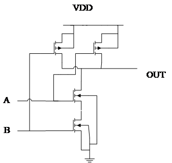
Figure 3: Schematic diagram of NAND gate.
Table 3: NAND gate truth table.
A | B | Y |
0 | 0 | 1 |
0 | 1 | 1 |
1 | 0 | 1 |
1 | 1 | 0 |
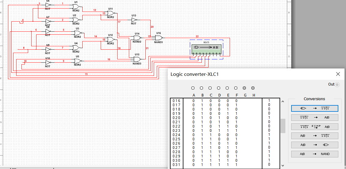
According to the target function of the comparator, the logic gates are combined together to realize the logic function and this design is designed and simplified using Karnaugh map. Figure 4 shows the circuit schematic of the comparator with two sets of three bits of data to be compared. The comparator works by comparing from the highest bit. When the highest bit of group A data is greater than the highest bit of group B data, it directly outputs ‘1’. If the highest bit of data in group A is equal to or less than the highest bit of data in group B, the comparison state with the highest bit goes to the second bit for comparison. This goes on and until the output is obtained, the comparison process is completed. When the data in group A is greater than the data in group B, the outcoming result is ‘1’. When the data in group A is less than or equal to the data in group B, the output result is ‘0’.
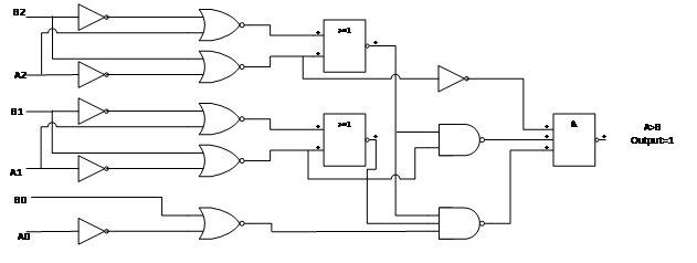
Figure 4: Comparator circuit schematic.
3. Performance optimization
The above digital comparator circuit is designed to realize the logic function of the circuit. Further, performance optimization of circuits is important in circuit design, including energy consumption optimization and delay optimization. There are several ways to optimize the power consumption of digital circuits, which also includes optimization of many levels: optimization of the topology of the circuit, optimization of the implementation algorithms, control of the voltage, and when there is no significant impact on the delay of the circuit, it can be achieved by lowering the supply voltage, which in turn reduces the power consumption [9]. Next, the digital comparator designed in this paper is optimized for power consumption from the certain angle of optimizing the supply voltage. The delay of the digital comparator circuit designed in this paper can be calculated from equations (1), (2), (3):
\( D=N{f^{*}}+p \) (1)
\( {f^{*}}=\sqrt[N]{F} \) (2)
\( F=GBH \) (3)
Where N is the order of the circuit, which depends on the number of stages of the gate circuit. F is the circuit Path Effort. p is the circuit Path Parasitic Delay. f is the circuit Path Effort Delay. G is the logical Effort. The energy consumption of the circuit can be calculated from equation (4).
\( {E_{0}}={C_{tot}}×{V_{DD}}{ ^{2}} \) (4)
As the supply voltage of the circuit decreases, the energy consumption of the circuit decreases, but at the same time the delay increases. Delay and energy consumption are somehow difficult to optimize at the same time. In order to optimize the supply voltage, this study optimizes the circuit's power use.
When the supply voltage of the circuit is 1V, the minimum delay is calculated. The energy consumption at this point is relatively high at 5.7128. So, the target performance optimized in this design is to reduce the energy consumption based on 1.5 times of the minimum delay. From the perspective of the supply voltage, the circuit is optimized. The optimized supply voltage can be calculated according to equations (5), (6):
\( D=k×\frac{{V_{DD}}}{({V_{DD}}-{V_{TH}}){ ^{2}}} \) (5)
\( 1.5D=k×\frac{V_{DD}^{opt}}{(V_{DD}^{opt}-{V_{TH}}){ ^{2}}} \) (6)
The optimized supply voltage can be calculated to be 0.7747V at 1.5 times delay. At this point, the energy consumption of the circuit after supply voltage optimization can be calculated. The optimized energy is 3.429. The reduction in energy consumption is 39.98%. It can be seen that optimizing the supply voltage can effectively optimize the circuit power consumption. Thus, power dissipation is greatly reduced when parts of the integrated circuit operate at lower voltages [10]. Nowadays, the low-voltage and low-power operating conditions of integrated circuits also place higher demands on the low-voltage design techniques of the circuits [11]. The requirements of digital integrated circuits tend to reduce voltage supply and increase integrated circuit performance.
4. Functional simulation
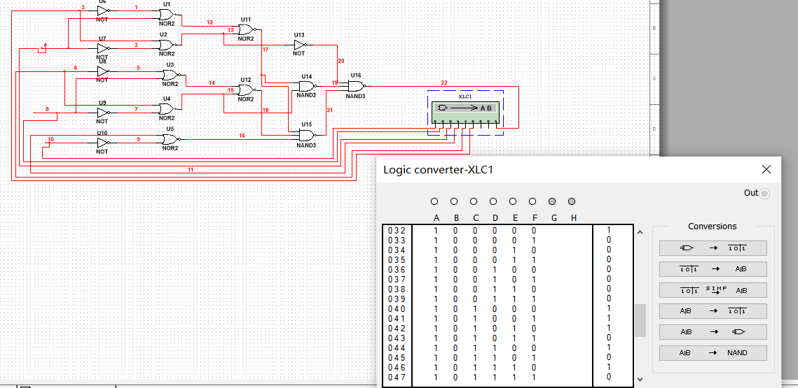
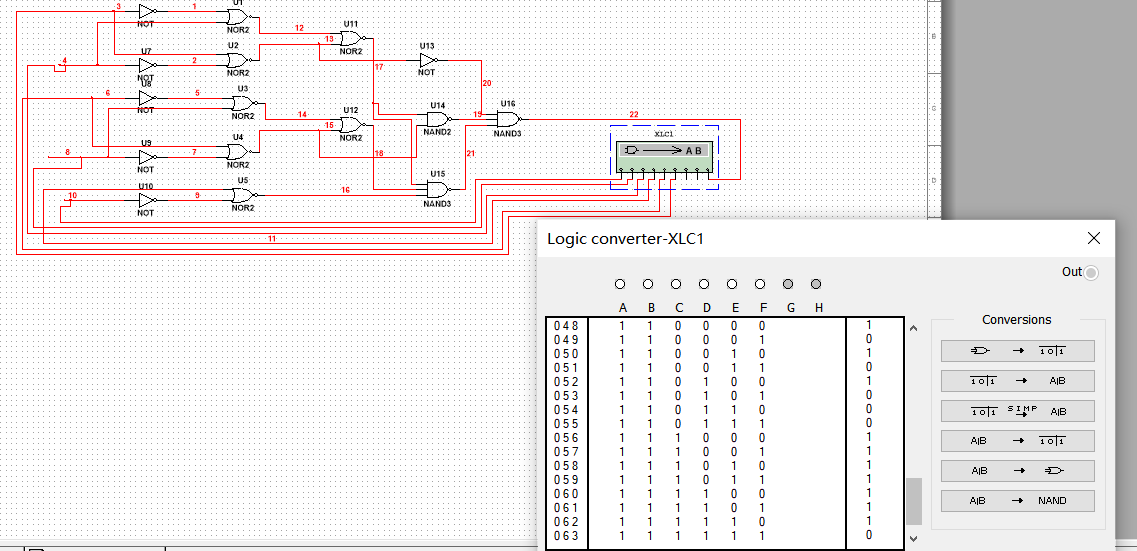
The digital comparator designed in this paper is simulated for the logic function of the digital comparator circuit. The comparator designed in this paper consists of 6 NOT gates, 7 NOR gates and 3 NAND gates. In figure 5, A represents the lowest bit of group A data, A0. B represents the second bit of group A data, A1. C represents the highest bit of group A data, A2. D represents the lowest bit of group B data, B0. E represents the second bit of group B data, B1. F represents the highest bit of group B data, B2. The functional simulation of the circuit can be seen as shown in figure 5(a), (b), (c), (d). In figure 5(a) the digital comparator designed in this paper has input values from 000000 to 001111. The input values of the digital comparator in figure 5(b) are from 010000 to 011111. The input values of the digital comparator in figure 5(c) are from 100000 to 101111. The digital comparator in figure 5(d) has input values from 110000 to 111111. The output is ‘1’ when the input Group A data is greater than Group B data, and ‘0’ when the input Group A data is less than or equal to Group B data. For example, when the provided value is 001000, the value from the outcoming port is ‘1’. When the entered data is 000001, the result signal is ‘0’.
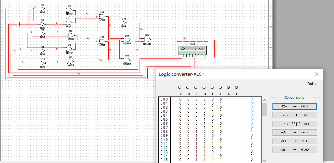
(a)
(b)
(c)
(d)
Figure 5: Comparator function simulation.
5. Conclusion
This paper analyzes the development trend of digital integrated circuits and the wide application of digital comparators and designs a three-bit digital comparator composed of CMOS logic gates. Functional simulation of the comparator, which is capable of numerical comparison, is carried out by Multisim. The digital comparator designed in this paper is optimized for energy consumption by reducing the supply voltage. In the future, it may be possible to optimize the digital comparator designed in this paper from more different perspectives, not only from the point of view of the supply voltage, but also by choosing to optimize the energy consumption from the point of view of the logic gate level, including the use of lower-power logic devices, the optimization of the logic of the comparator, and the adjustment of the transistor size. This is a direction for improvement in the future.
References
[1]. Wendong Jiang .Low Power Digital Integrated Circuit Design[D].Beijing Jiaotong University,2008.
[2]. Hu W .Review on low power design of digital integrated circuits[J].Journal of Physics: Conference Series,2024,2798(1):012047-012047.
[3]. Yewale S , Gamad R .Design of Low Power and High Speed CMOS Comparator for A/D Converter Application[J].Wireless Engineering and Technology, 2012, 03(2):90-95.
[4]. I N G ,V V B ,B V B .A Tutorial Review on the Fluorescent Probes as a Molecular Logic Circuit-Digital Comparator.[J].Molecules (Basel, Switzerland),2023,28(17):
[5]. Kumar A M .A Low Power Digital Binary Magnitude Comparator Design for Very Large Scale Integration Applications[J].Advanced Science, Engineering and Medicine,2020,12(6):825-830.
[6]. Dengyu Zhang,Yongkang Tan. Classical Logic Gates and Quantum Logic Gates[J]. Journal of Hengyang Normal University, 2019, 40 (03): 16-23.
[7]. Feifei Mao.CMOS Digital Circuit Based on Two dimensional Transition Metal Dichalcogenide Transistors[D].East China Normal University,2020.
[8]. Muyao Ruan. Research on Energy Efficiency of Logic Gates and Parity Check Circuit Based on Information Thermodynamics[D].Huazhong University of Science and Technology,2023.
[9]. Chandrakasan, A. P., & Brodersen, R. W. (1995). Minimizing power consumption in digital CMOS circuits. Proceedings of the IEEE, 83(4), 498-523.
[10]. Ahmed F U, Sandhie Z T, Ali L, et al. A brief overview of on-chip voltage regulation in high-performance and high-density integrated circuits[J]. IEEE Access, 2020, 9: 813-826.
[11]. Rakús M, Stopjaková V, Arbet D. Design techniques for low-voltage analog integrated circuits[J]. Journal of Electrical Engineering, 2017, 68(4): 245-255.
Cite this article
Lu,X. (2025). Multisim-Based Digital Comparator Design and Performance Optimization. Applied and Computational Engineering,127,16-23.
Data availability
The datasets used and/or analyzed during the current study will be available from the authors upon reasonable request.
Disclaimer/Publisher's Note
The statements, opinions and data contained in all publications are solely those of the individual author(s) and contributor(s) and not of EWA Publishing and/or the editor(s). EWA Publishing and/or the editor(s) disclaim responsibility for any injury to people or property resulting from any ideas, methods, instructions or products referred to in the content.
About volume
Volume title: Proceedings of the 5th International Conference on Materials Chemistry and Environmental Engineering
© 2024 by the author(s). Licensee EWA Publishing, Oxford, UK. This article is an open access article distributed under the terms and
conditions of the Creative Commons Attribution (CC BY) license. Authors who
publish this series agree to the following terms:
1. Authors retain copyright and grant the series right of first publication with the work simultaneously licensed under a Creative Commons
Attribution License that allows others to share the work with an acknowledgment of the work's authorship and initial publication in this
series.
2. Authors are able to enter into separate, additional contractual arrangements for the non-exclusive distribution of the series's published
version of the work (e.g., post it to an institutional repository or publish it in a book), with an acknowledgment of its initial
publication in this series.
3. Authors are permitted and encouraged to post their work online (e.g., in institutional repositories or on their website) prior to and
during the submission process, as it can lead to productive exchanges, as well as earlier and greater citation of published work (See
Open access policy for details).
References
[1]. Wendong Jiang .Low Power Digital Integrated Circuit Design[D].Beijing Jiaotong University,2008.
[2]. Hu W .Review on low power design of digital integrated circuits[J].Journal of Physics: Conference Series,2024,2798(1):012047-012047.
[3]. Yewale S , Gamad R .Design of Low Power and High Speed CMOS Comparator for A/D Converter Application[J].Wireless Engineering and Technology, 2012, 03(2):90-95.
[4]. I N G ,V V B ,B V B .A Tutorial Review on the Fluorescent Probes as a Molecular Logic Circuit-Digital Comparator.[J].Molecules (Basel, Switzerland),2023,28(17):
[5]. Kumar A M .A Low Power Digital Binary Magnitude Comparator Design for Very Large Scale Integration Applications[J].Advanced Science, Engineering and Medicine,2020,12(6):825-830.
[6]. Dengyu Zhang,Yongkang Tan. Classical Logic Gates and Quantum Logic Gates[J]. Journal of Hengyang Normal University, 2019, 40 (03): 16-23.
[7]. Feifei Mao.CMOS Digital Circuit Based on Two dimensional Transition Metal Dichalcogenide Transistors[D].East China Normal University,2020.
[8]. Muyao Ruan. Research on Energy Efficiency of Logic Gates and Parity Check Circuit Based on Information Thermodynamics[D].Huazhong University of Science and Technology,2023.
[9]. Chandrakasan, A. P., & Brodersen, R. W. (1995). Minimizing power consumption in digital CMOS circuits. Proceedings of the IEEE, 83(4), 498-523.
[10]. Ahmed F U, Sandhie Z T, Ali L, et al. A brief overview of on-chip voltage regulation in high-performance and high-density integrated circuits[J]. IEEE Access, 2020, 9: 813-826.
[11]. Rakús M, Stopjaková V, Arbet D. Design techniques for low-voltage analog integrated circuits[J]. Journal of Electrical Engineering, 2017, 68(4): 245-255.