


1. Introduction
The invention of the point-contact transistor by Bell Labs in 1947 marked the beginning of the semiconductor era. In 1958, Texas Instruments developed the world's first digital integrated circuit, which was a significant milestone in the history of integrated circuits. Subsequently, Fairchild Semiconductor proposed two key processes, namely lithography and planar processing, which built the foundation for the mass production of integrated circuits. Integrated circuits have become a fundamental component of modern information technology.
With the development of technology, the size of integrated circuits is getting smaller and smaller, the integration density is getting higher and higher, which has promoted the progress of computers, communications, and consumer electronics. Integrated circuits support the development of the world economy. The wide use of integrated circuits has changed people's lifestyles, from smartphones and tablets to smart electrical appliances and smart transportation. Integrated circuits have entered every aspect of people's lives. These electronic goods have not only improved the quality of people's life, but also changed their communication style, consumption habits, and working habits.
Semiconductor is the foundation for manufacturing integrated circuits, and the development of semiconductor has driven the development of integrated circuits. With the continuous optimization and innovation of semiconductor technology, the integration density of integrated circuits continues to increase, the performance continues to enhance, and the power consumption continues to decrease, which promotes the development of the entire electronics industry. This paper analyzes the development history and current state of semiconductors, forecasts the development trend of semiconductors.
2. Development history of semiconductor
In 1904, British physicist John Ambrose Fleming invented the first vacuum diode.
In 1906, American engineer Lee de Forest invented the vacuum transistor making the electronic tube the ability to amplify and oscillate. This invention was the birth of the electronics industry.
On December 6, 1947, William Shockley, John Bardeen, and Walter Brattain invented the world's first germanium point-contact transistor at Bell Laboratories in Murray Hill, New Jersey, USA[1]. The transistor is one of the greatest inventions in modern history, which made electronic products such as radios, calculators, and computers smaller and cheaper, and had great significance for the development of integrated circuits.
In April 1950, Shockley made the first bipolar junction transistor - the PN junction transistor. Today most transistors are still PN junction transistors.
In 1952, the junction field effect transistor was manufactured [1].
In 1959, Atara and others invented a Metal Oxide Semiconductor.
In 1963, Frank and C.T. Sah first proposed CMOS (Complex Metal Oxide Semiconductor) technology, which connected n-MOS and p-MOS into a complementary structure. This bipolar mosfet was almost free of static current when they were in and on state, so they were suitable for logic circuits. CMOS technology has the advantages of low power, high integration density, and easy production. Since the 1970s and 1980s, it has gradually become the mainstream process for integrated circuit chip production. Until now, this technology has occupied more than 95% of the global semiconductor integrated circuit chip industry [2].
When mentioning semiconductors, the first thing that comes to mind is Moore's Law. In 1965, Gordon Moore proposed Moore's Law. Moore's Law states that when prices remain constant, the number of transistors in a chip will double approximately every 18 months, and the performance will increase twice. The development of CMOS effectively validates the accuracy of Moore's Law.
Table 1 shows the transistor densities of Intel 90nm, 65nm, 45nm, 32nm, 22nm, 14nm, 10nm, and 7nm process nodes. The data in Table 1 also validates the accuracy of Moore's Law.
Table 1: Transistor density in intel process node
Process Node | 90nm | 65nm | 45nm | 32nm | 22nm | 14nm | 10nm | 7nm |
Density (MTr/mm2) | 1.45 | 2.08 | 3.33 | 7.11 | 16.5 | 44.67 | 100.76 | 212.48 |
The essence of Moore's Law is increasing transistor operating speed, increasing transistor density, and decreasing costs by reducing transistor feature size. However, as the feature size of transistors continues to decrease proportionally, the distance between the source and drain also becomes shorter. The channel is not only affected by the gate electric field but also by the source electric field. The control ability of the gate over the channel decreases, and the difficulty of the gate voltage clamping off the channel increases. This can easily result in leakage and the formation of the Short Channel Effect (SCE), which can cause serious degradation of the transistor and affect switching speed . Due to the above issues, it is difficult to further reduce the feature size of planar transistors. In 1999, Professor Hu Zhengming from the University of California, Berkeley invented FinFET (Fin Field Effect Transistor), which is a new type of three-dimensional transistor structure. This invention pioneered a new era of MOS structures. In 2009, Intel was the first to adopt this technology, and the 22nm process node released in 2011 was the industry's first process to use FinFET transistors.
FinFET has been used as a transistor in cutting-edge semiconductors for over a decade since 2011. But By 2022, when 5nm process node was in production, FinFET also faced problem such as leakage, short channel effect, and threshold voltage drift which due to transistor size shrinking[3].In order to solve these problems and the evolution of Moore's Law, it is urgent for the emergence of new transistors.
In 1990, Dr. Cor Claeys and his research team from IMEC in Belgium proposed the GAA technology.Compared to FinFET, transistors using GAA technology have stronger gate control over the channel. Currently, GAA has become the focus of attention in the semiconductor industry.
3. Current state of semiconductor process
Table 2 lists the most advanced process nodes of Intel, Samsung, and TSMC, the three most advanced semiconductor manufacturers in the world. Table 2 shows that FinFET has become the mainstream technology in advanced process nodes today. Samsung adopted GAA technology at the 3nm process node, making it the first semiconductor company in the industry to adopt GAA technology.
Table 2: Current status of advanced technologies from Intel, Samsung, TSMC
Intel | Samsung | TSMC | |||||||||
Process Node | 14nm | 10nm | 7nm | 10nm | 7nm | 5nm | 3nm | 10nm | 7nm | 5nm | 3nm |
FinFET | FinFET | FinFET | FinFET | FinFET | FinFET | GAA | FinFET | FinFET | FinFET | FinFET | |
This chapter focuses on FinFET and GAA, which are currently the two mainstream transistors.
The 3D structural schematic of FinFET is shown in Figure 1. The channel of FinFET is composed of high and thin fins protruding from the substrate, and the drain and source are located on both sides. Compared with the planar transistor, the FinFET solid fin structure enhances the gate's control ability over the channel and has significant advantages in controlling short channel effects, improving subthreshold characteristics, and suppressing gate leakage current.
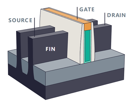
Figure 1: The schematic of FinFET transistor structure[4]
The invention of FinFET transistor is a significant technological breakthrough with high practical application value. It not only solves the leakage problem in the semiconductor process, but also promotes the continuation of Moore's Law, enabling the rapid development of electronic products. Since 2011, mobile electronic products have entered a stage of rapid development, and smartphones are the core of mobile electronic products, providing various functions such as communication and entertainment. The development of smartphones benefits from the advancement of semiconductor technology, which enables more transistors integrated into core components such as processors and memory in smartphones, thereby improving performance. And, the advanced semiconductor technology also helps to reduce the power consumption of chips and extend the battery life of smartphones. In addition, with the continuous reduction of chip size, smartphones can achieve thinner and lighter designs. The process node used by Apple smartphone SOC chips is shown in table 3. The SOC chips of iPhone15 Pro, iPhone15 Pro Max, and iPhone16 series smartphones all use the most advanced TSMC 3nm FinFET technology
Table 3: The process node of Apple Smartphone SOC chip
Year | Phone Type | SOC Chip | Foundry | Process Node |
2010 | iPhone4 | A4 | Samsung | 45nm |
2011 | iPhone4S | A5 | Samsung | 45nm |
2012 | iPhone5 | A6 | Samsung | 32nm |
2013 | iPhone5S | A7 | Samsung | 28nm |
2014 | iPhone6 | A8 | TSMC | 20nm |
2015 | iPhone6S | A9 | Samsung/TSMC | 14nm/16nm |
2016 | iPhone7 | A10 | TSMC | 16nm+ |
2017 | iPhoneX | A11 | TSMC | 10nm |
2018 | iPhoneXs | A12 | TSMC | 7nm |
2019 | iPhone11 Pro | A13 | TSMC | 7nm |
2020 | iPhone12 Pro | A14 | TSMC | 5nm |
2021 | iPhone13 Pro | A15 | TSMC | 5nm |
2022 | iPhone14 Pro | A16 | TSMC | 4nm |
2023 | iPhone15 Pro | A17 | TSMC | 3nm |
2024 | iPhone16 Pro | A18 | TSMC | 3nm |
Gate-All-Around(GAA) is a gate all around the 3D transistor[5]. In this transistor, the gate completely surrounds the source and drain, forming four contact surfaces and improving the control ability of the channel.
GAA is further divided into nanowires (shown in Figure 2) and nanosheet (shown in Figure 3) due to the different channel shapes. The channel shape of nanowire is a slender linear shape, while the channel shape of nanosheet is a flat sheet shape, with a larger contact area between the gate and the channel. Because nanosheet has wider channels, they have stronger driving currents and better performance than nanowire.
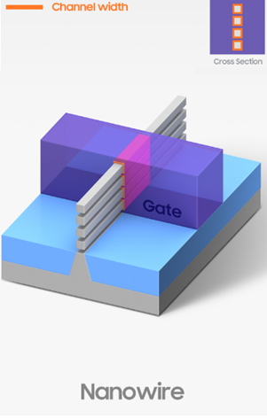
Figure 2: The schematic of nanowire structured transistor[6]
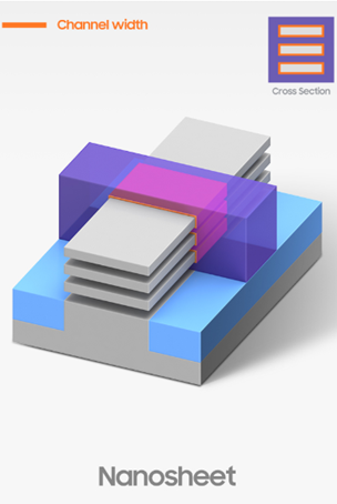
Figure 3: The schematic of nanosheet structured transistor[6]
4. The trend of the semiconductor process
Due to the reduction in transistor feature size approaching the physical limit, the cost of developing and producing smaller chips is also increasing, and the manufacturing cycle time is also getting longer. The industry and academia are exploring new solution to address the slowdown of Moore's Law. Now there are three solutions that have made progress. The first solution is the new transistor technologies, such as Forksheet [7] and Complementary-FET[8], which are currently under research. The second solution is DTCO (Design Technology Co optimization), which improves the density of transistors per unit area without changing the feature size of the transistors. The third solution is 3DIC, which achieves the goal of integrating more transistors in a smaller space by stacking multiple dies together.
DTCO is a relatively mature technology, such as TSMC achieving an increase in transistor density through DTCO at multiple advanced process nodes. This chapter focuses on DTCO technology.
The definition of DTCO is quite broad, and any co-optimization measures between the semiconductor process and specific circuit designs can be referred to as DTCO. Generally speaking, conventional semiconductor chip design involves optimizing circuit design based on the given process and PDK(process design kit). Therefore, in the context of recent years, DTCO mainly refers to how to optimize semiconductor process according to the specific requirements of semiconductor chips. Specific process optimization can include materials for metal interconnects, via design, specific CMOS device design, and so on.
In the golden age of Moore's Law, as a new generation of semiconductor processes emerges every year with significant performance improvements, the benefits of spending a lot of time and resources on DTCO optimization for this generation of processes are not significant. However the continuation of Moore's Law is becoming more and more challenging, and the cost of developing and using new-generation semiconductor process is getting higher. At the same time, the performance improvement brought by the new-generation semiconductor process is getting smaller and smaller. It is more practical to use DTCO to optimize semiconductor processes and circuit design.
Figure 4 shows the proportion of DTCO contribution to transistor density increasing in TSMC at 16nm, 10nm, 7nm, 5nm, and 3nm process nodes.
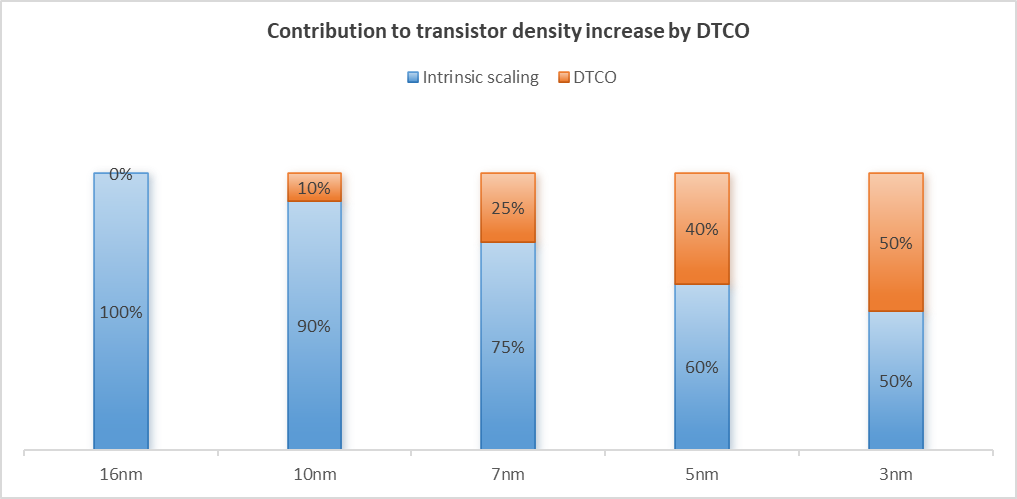
Figure 4: Contribution to transistor density increase by DTCO[9]
Now, DTCO plays a crucial role in the semiconductor process and is one of the key technologies driving the continuous progress and development of the semiconductor industry. Here are a few examples of using DTCO technology to increase the density of unit transistors[10].
4.1. DDB to SDB
Diffusion Break(DB) is used in a standard cell to isolate two adjacent devices, prevent diffusion currents between adjacent devices from affecting each other, and ensure the stability and stability of the devices.
Double Difufsion Break(DDB)is a design where adjacent devices have independent Shllow Trench Isolation(STI), providing good isolation while also increasing the width of standard cells, as shown in Figure 5.
Single Diffusion Break (SDB), where adjacent devices share STI, reduces the standard cell width to increase transistor density, as shown in Figure 6.
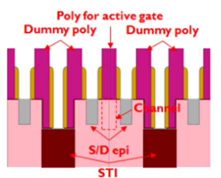
Figure 5: DDB[11]
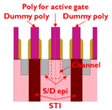
Figure 6: SDB[11]
4.2. COAG
COAG technology is that gate contact point is the control point for the source drain current in a transistor. Figure 7 is a traditional top view of a transistor. Figure 8 is a top view of a transistor using COAG technology. Placing the "gate contact" directly above the "active" area of the transistor can save space and enable the integration of more transistors in the same area. Intel 10nm process node used COAG technology, resulting in a reduction of approximately 10% in area. Due to the close contact between the gate and the contact point, COAG technology can improve the performance of transistors, including response speed and stability.
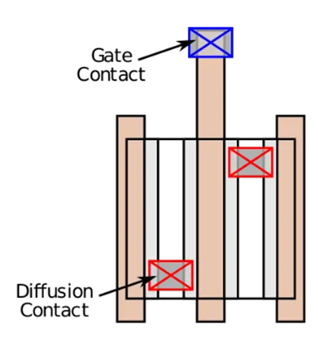
Figure 7: Top view of traditional transistor[12]
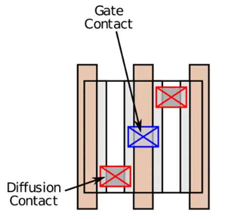
Figure 8: Top view of transistor using COAG technology [12].
Although COAG can bring benefits in terms of area and performance, it also faces some challenges. Firstly, the implementation of COAG technology requires precise process control, including photolithography, etching, and ion implantation, which increases the difficulty and cost of manufacturing; Secondly, due to the close contact between the gate and the contact point, COAG technology may lead to some manufacturing difficulties and yield issues that require further optimization and improvement.
4.3. Fin depopulation
Fin depopulation technology reduces the height of transistors by decreasing the number of Fins, allowing for the integration of more transistors per unit area. This technology can reduce power consumption and increase transistor density by reducing the number of Fins without sacrificing too much performance. Figure 9 is a schematic diagram of reducing the transistor height by decreasing the number of Fins inside the transistor.
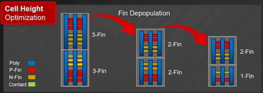
Figure 9: Schematic diagram of reducing the transistor height by decreasing Fin number[8]
Although Fin depopulation technology has the above advantages, it also faces some challenges in the manufacturing process. Firstly, reducing the number of Fins and lowering the height of transistors requires higher process control accuracy to ensure the performance and reliability of transistors. Secondly, Fin depopulation technology requires more complex designs to ensure the integrity of connections and signal transmission between transistors.
5. Conclusion
From the development of semiconductor process, it can be seen that from invention to mass production of new structured transistors takes several years, which involves multiple complex tasks, including research and development, testing, optimization, and production line preparation. Each task requires a significant investment of time, manpower, and material resources. The development of new structure transistors such as Forksheet and Complementary-FET is still in the research stage, and the time for mass production is uncertain. In order to ensure the continued evolution of Moore's Law, it is essential to pursue the development of new structure transistors while also exploring alternative avenues, such as the utilisation of novel materials and 3DIC to enhance the density of unit space transistors. The preceding analysis has identified DTCO as the most advanced technology for augmenting transistor density and performance, with extensive deployment across multiple process nodes, thereby offering promising avenues for the advancement of semiconductor processing.
References
[1]. Ukasiak, L. & Jakubowski, A. (2010). History of semiconductors. journal of telecommunications & information technology.
[2]. Mack, C. A. (2011). Fifty years of moore's law. IEEE Transactions on Semiconductor Manufacturing, 24(2), 202-207.
[3]. Banna, S. (2015). Scaling challenges of FinFET technology at advanced nodes and its impact on SoC design (Invited). Custom Integrated Circuits Conference (pp.1-8).
[4]. https://lamreserach.com/zh-hans/products/our-solutions/transistor-solutions/?Highlight=FinFET
[5]. Zhang, J. (2022). A review of the gate-all-around nanosheet fet process opportunities. Electronics, 11.
[6]. https://semiconductor.samsung.com/cn/news-events/tech-blog/gaa-dtco-for-ppa/
[7]. Mertens, H. Ritzenthaler, R. , Oniki, Y., Briggs, B. , Chan, B. T.,& Hikavyy, A., et al. Forksheet FETs for Advanced CMOS Scaling: Forksheet-Nanosheet Co-Integration and Dual Work Function Metal Gates at 17nm N-P Space. 2021 Symposium on VLSI Technology. IEEE.
[8]. Zhang, K. 1.1 Semiconductor Industry: Present & Future. 2024 IEEE International Solid-State Circuits Conference (ISSCC). IEEE.
[9]. Liu, M. (2021). 1.1 unleashing the future of innovation. IEEE.
[10]. Heo, S. I. Kahng, A. B. Kim, M. , & Wang, L. (2019). Diffusion break-aware leakage power optimization and detailed placement in sub-10nm vlsi.
[11]. K. Miyaguchi, F. M. Bufler, T. Chiarella, P. Matagne, N. Horiguchi, A. De Keersgieter, G. Eneman, A. Spessot, *B. Parvais, D. Verkest and A. Mocuta. (2017). Single and Double Diffusion Breaks in 14nm FinFET and Beyond
[12]. https://en.wikichip.org/wiki/contact_over_active_gate.
Cite this article
Qi,X. (2025). The Development History and Evolutionary Trends of Semiconductor. Applied and Computational Engineering,125,222-230.
Data availability
The datasets used and/or analyzed during the current study will be available from the authors upon reasonable request.
Disclaimer/Publisher's Note
The statements, opinions and data contained in all publications are solely those of the individual author(s) and contributor(s) and not of EWA Publishing and/or the editor(s). EWA Publishing and/or the editor(s) disclaim responsibility for any injury to people or property resulting from any ideas, methods, instructions or products referred to in the content.
About volume
Volume title: Proceedings of the 3rd International Conference on Mechatronics and Smart Systems
© 2024 by the author(s). Licensee EWA Publishing, Oxford, UK. This article is an open access article distributed under the terms and
conditions of the Creative Commons Attribution (CC BY) license. Authors who
publish this series agree to the following terms:
1. Authors retain copyright and grant the series right of first publication with the work simultaneously licensed under a Creative Commons
Attribution License that allows others to share the work with an acknowledgment of the work's authorship and initial publication in this
series.
2. Authors are able to enter into separate, additional contractual arrangements for the non-exclusive distribution of the series's published
version of the work (e.g., post it to an institutional repository or publish it in a book), with an acknowledgment of its initial
publication in this series.
3. Authors are permitted and encouraged to post their work online (e.g., in institutional repositories or on their website) prior to and
during the submission process, as it can lead to productive exchanges, as well as earlier and greater citation of published work (See
Open access policy for details).
References
[1]. Ukasiak, L. & Jakubowski, A. (2010). History of semiconductors. journal of telecommunications & information technology.
[2]. Mack, C. A. (2011). Fifty years of moore's law. IEEE Transactions on Semiconductor Manufacturing, 24(2), 202-207.
[3]. Banna, S. (2015). Scaling challenges of FinFET technology at advanced nodes and its impact on SoC design (Invited). Custom Integrated Circuits Conference (pp.1-8).
[4]. https://lamreserach.com/zh-hans/products/our-solutions/transistor-solutions/?Highlight=FinFET
[5]. Zhang, J. (2022). A review of the gate-all-around nanosheet fet process opportunities. Electronics, 11.
[6]. https://semiconductor.samsung.com/cn/news-events/tech-blog/gaa-dtco-for-ppa/
[7]. Mertens, H. Ritzenthaler, R. , Oniki, Y., Briggs, B. , Chan, B. T.,& Hikavyy, A., et al. Forksheet FETs for Advanced CMOS Scaling: Forksheet-Nanosheet Co-Integration and Dual Work Function Metal Gates at 17nm N-P Space. 2021 Symposium on VLSI Technology. IEEE.
[8]. Zhang, K. 1.1 Semiconductor Industry: Present & Future. 2024 IEEE International Solid-State Circuits Conference (ISSCC). IEEE.
[9]. Liu, M. (2021). 1.1 unleashing the future of innovation. IEEE.
[10]. Heo, S. I. Kahng, A. B. Kim, M. , & Wang, L. (2019). Diffusion break-aware leakage power optimization and detailed placement in sub-10nm vlsi.
[11]. K. Miyaguchi, F. M. Bufler, T. Chiarella, P. Matagne, N. Horiguchi, A. De Keersgieter, G. Eneman, A. Spessot, *B. Parvais, D. Verkest and A. Mocuta. (2017). Single and Double Diffusion Breaks in 14nm FinFET and Beyond
[12]. https://en.wikichip.org/wiki/contact_over_active_gate.