


1. Introduction
In the contemporary era marked by an escalating global energy consumption and the dynamic evolution of power electronics technologies, the pursuit of high-efficiency and high-reliability power devices has garnered extensive attention within the scientific and industrial communities. Silicon carbide (SiC), a semiconductor material characterized by a wide-bandgap, emerges at the forefront of this research, showcasing profound potential for revolutionizing power electronics owing to its distinguished physical attributes and superior operational capabilities [1-3].
Silicon carbide devices are predominantly celebrated for their exceptional thermal stability, a trait that can be ascribed to their high thermal conductivity [4]. This intrinsic property enables SiC devices to effectively dissipate heat, thereby operating at lower temperatures and reducing the dependency on elaborate cooling systems. Such a reduction is instrumental in facilitating the miniaturization of power electronic systems, thus meeting modern demands for compact yet powerful electronic components [5]. Additionally, the robust crystal structure and expansive bandgap of SiC contribute to consistent performance under elevated temperatures, significantly surpassing traditional silicon-based devices in high-temperature applications. This inherent stability and resilience open up a spectrum of applications for SiC devices in areas such as new energy vehicles, high-speed railway systems, and solar power inverters, where reliability under harsh conditions is critical.
The considerable bandgap of SiC not only enhances its thermal characteristics but also permits device operation at elevated temperatures, potentially reaching up to 300°C. This capability introduces unprecedented opportunities for deploying these devices in environments that experience extreme temperatures, which traditionally challenge the reliability and efficiency of conventional semiconductor materials. Furthermore, SiC devices exhibit remarkable electron saturation drift velocity, which facilitates high switching speeds and minimal energy losses during power conversion processes. These features are critical for improving the efficiency and performance of power electronic systems. Moreover, the enhanced breakdown voltage and compact form factor of SiC devices allow for a significant reduction in the size of passive filtering components within converters. This compactness contributes to decreased conduction losses, which is a pivotal factor in enhancing the overall efficiency of power systems [6-8].
Despite the myriad advantages presented by SiC technology, several formidable challenges impede its widespread adoption in practical settings. Among the predominant concerns is the vulnerability to short-circuit failures, often triggered by anomalous gate turn-on events. These events abruptly expose the SiC MOSFET’s drain-source terminals to the bus voltage, precipitating thermal failures and jeopardizing device integrity, particularly in high-power deployments. The absence of rapid and effective short-circuit protection mechanisms remains a critical barrier to the broader application of SiC devices in power electronics [9]. Furthermore, avalanche failures present a significant threat, especially in scenarios involving non-clamped stress switching. Here, the inductive loads can induce excessively high voltages across the device during circuit deactivation, forcing the SiC into an avalanche breakdown state. Additionally, the high-speed switching operations may result in electrical interference from adjacent complementary transistors, alongside interactions between the main power loop and the driving circuitry, posing further risks to device stability and operational safety. These technical challenges not only test the robustness and dependability of SiC devices but also elevate the technical requirements for their integration into advanced power electronic systems [10].
This paper delves into the issues of short-circuit and avalanche failures peculiar to SiC MOSFETs, providing a comprehensive examination of the technical hurdles that limit their functionality. Section 2 elucidates on the pivotal failure modes—short-circuit and avalanche failures, encountered in high-voltage and high-power applications, discussing their detrimental effects on the reliability and stability of the devices. Section 3 proposes and explores innovative design strategies aimed at bolstering the reliability of SiC MOSFETs, ensuring their operational integrity under adverse conditions. Finally, Section 4 encapsulates the essence of the research undertaken, accentuating key findings while paving the way for future inquiries into the mitigation of these critical issues, thereby fostering the development of more resilient and efficient power electronic systems.
2. SiC MOSFET Failure Issues
Silicon Carbide (SiC) devices, owing to their superior thermal and electrical properties, have emerged as a significant contender in the arena of power electronics. Despite their promising potential, SiC devices face persistent challenges in terms of reliability and stability, which are critical to their performance and applicability in real-world scenarios. This paper intricately examines two predominant failure modes that afflict SiC MOSFETs—short-circuit failure and avalanche failure under non-clamped stress switching conditions. These failures impose profound limitations on the deployment of SiC MOSFETs in environments demanding high-voltage and high-power performance.
2.1. SiC MOSFET Short-Circuit Failure
Silicon Carbide Metal-Oxide-Semiconductor Field-Effect Transistors (MOSFETs) are critical components in modern power electronic systems, boasting superior properties such as high thermal conductivity, elevated breakdown voltages, and swift switching capabilities. Despite these advantages, SiC MOSFETs are particularly susceptible to short-circuit failures, a severe reliability concern that impedes their broader application in high-power electronics.
Short-circuit failure in SiC MOSFETs typically results from an abnormal activation of the gate, leading to instantaneous application of bus voltage across the drain-source terminals. This event triggers a dramatic surge in current, often exceeding the device's rated current by multiple factors, sometimes by tens of times the normal operational current. This abrupt increase in current flow results in excessive heat generation within the device, culminating in a thermal failure if not mitigated promptly.
The management of these short-circuit events poses significant challenges. Although SiC materials inherently possess higher thermal conductivity compared to traditional silicon (Si) materials—facilitating improved heat dissipation—the rapid onset of extreme temperatures during short-circuits demands exceptionally brief response times for protective measures. Consequently, developing reliable, fast-acting, and efficient short-circuit protection schemes becomes crucial. The absence of such protection technology severely limits the practical deployment of SiC MOSFETs in applications demanding high power handling and reliability.
Moreover, the design constraints associated with SiC MOSFETs, such as their smaller chip size at equivalent current ratings compared to Si devices, result in higher current densities under fault conditions. This elevated current density exacerbates the thermal management challenge, necessitating even more robust short-circuit protection strategies.
Addressing these challenges is vital for advancing the use of SiC MOSFETs in critical power applications. Enhancements in device design, coupled with innovative approaches in circuit protection, are essential to overcome the limitations posed by short-circuit vulnerabilities. Only through such advancements can the full potential of SiC technology be realized in the field of power electronics, ensuring device safety, reliability, and efficiency in high-stakes environments.
Figure 1 illustrates the on-state characteristics and transfer characteristics of SiC MOSFETs:
|
|
(a) | (b) |
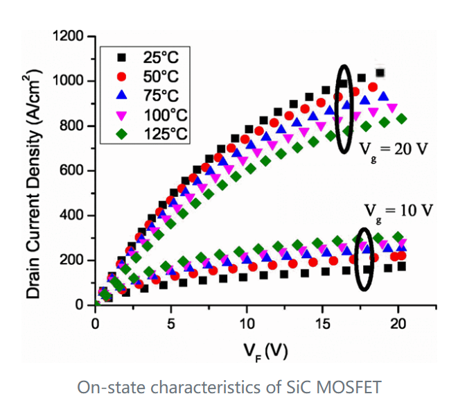
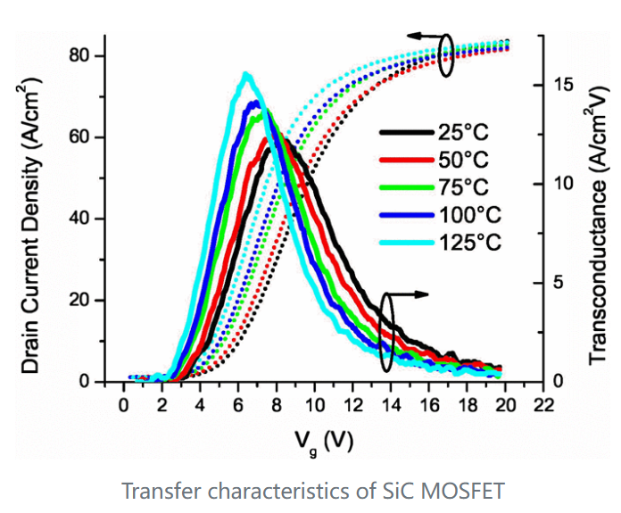
Figure 1: (a) On-state characteristics of SiC MOSFET (b): Transfer characteristics of SiC MOSFET [11]
Extracting and Analyzing Data from the On-state Characteristics Graph of SiC MOSFET:
Figure 2(a) illustrates the changes in the output characteristics of the SiC MOSFET at a fixed gate voltage 𝑉𝑔=10𝑉 under different temperatures of 25°C, 50°C, 75°C, 100°C, and 125°C.
|
|
(a) | (b) |
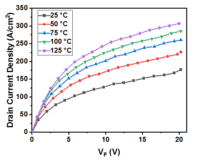
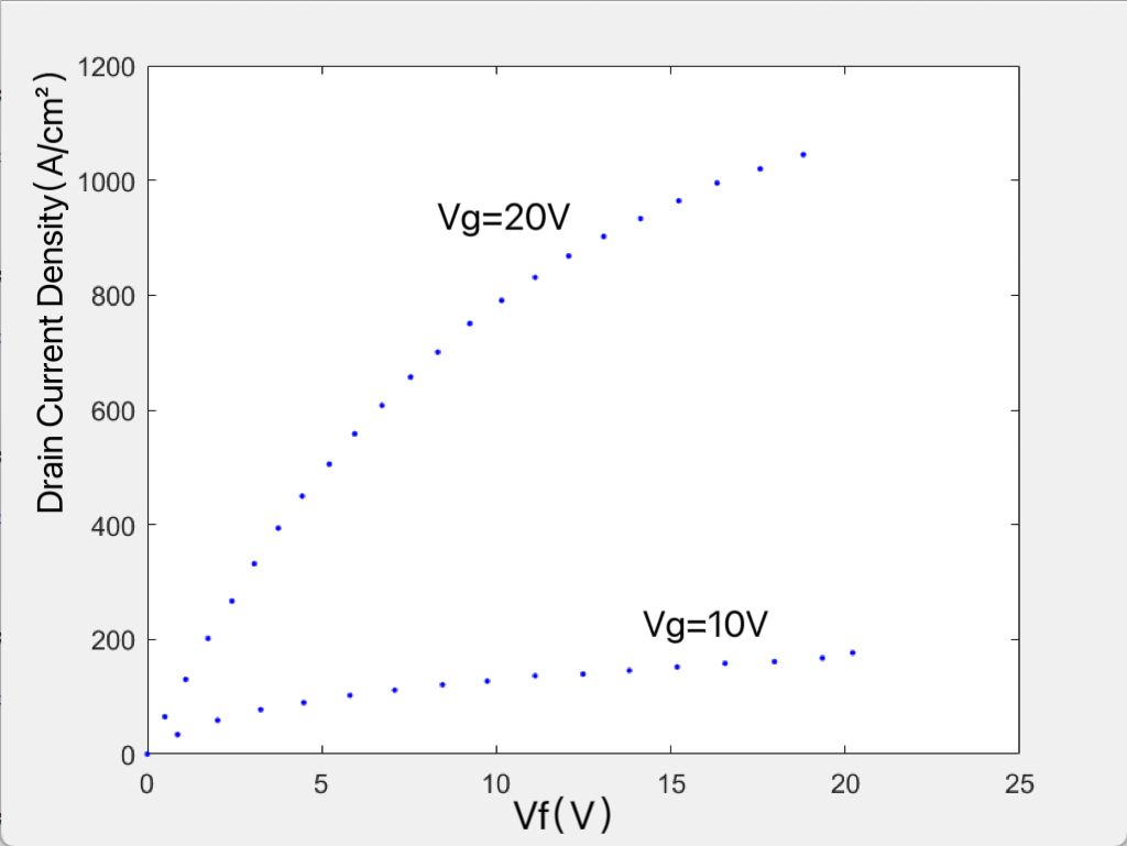
Figure 2: (a) On-state characteristics of SiC MOSFET, fixed 𝑉𝑔=10𝑉 (b) On-state characteristics at 𝑉𝑔=10𝑉 and 𝑉𝑔=20𝑉
By analyzing Figure 2(a), it can be observed that at a fixed gate voltage 𝑉𝑔=10𝑉, the current density increases gradually as the temperature rises.
Figure 2(b) shows the on-state characteristic curves of the SiC MOSFET at a temperature of 25°C when the gate voltage 𝑉𝑔 is 10V and 20V, respectively.
From the analysis of Figure 2(b), it is evident that when the temperature is constant, an increase in the gate voltage 𝑉𝑔 leads to a corresponding increase in current density. Moreover, the impact of increasing 𝑉𝑔 on current density is more significant than that of temperature.
2.2. SiC MOSFET Avalanche Failure
Avalanche failure is a critical reliability issue in Silicon Carbide (SiC) devices, particularly under scenarios where non-clamped inductive switching occurs. This type of failure generally manifests during the turn-off phase in circuits that handle high voltage differentials across the drain-source terminals of SiC Metal-Oxide-Semiconductor Field-Effect Transistors (MOSFETs). The presence of inductive loads substantially influences this phenomenon by inducing a high voltage scenario during the switching process.
During the non-clamped inductive switching events, the energy stored in the circuit's inductor is abruptly released and imposed onto the SiC device. If this discharged energy surpasses the avalanche energy tolerance of the device—a threshold indicating the maximum energy the device can absorb without undergoing destructive breakdown—an avalanche failure is likely to occur. Avalanche breakdown is a state where the device cannot restrict the flow of current caused by the extreme electric field within it, leading to thermal and electrical overstress.
In real-world applications, especially in systems characterized by high-frequency and high-power usage, SiC devices are often subjected to these harsh operational conditions. The impact of such stress on the integrity and functionality of SiC MOSFETs is substantial, demanding robust protective measures to mitigate potential failures.
Notwithstanding the inherent superior electrical and thermal properties of SiC materials—such as high thermal conductivity and high breakdown voltage—there remains a pressing need to enhance the avalanche tolerance of these devices. This enhancement could be achieved through meticulous design improvements targeting internal device structures. Additionally, optimizing external circuit protection mechanisms is crucial. Such advancements may include the implementation of active clamping techniques or the integration of snubber circuits, which can effectively manage sudden voltage spikes and dissipate excess energy.
To ensure the stable and reliable operation of SiC MOSFETs in demanding environments, ongoing research and development must focus on both improving the intrinsic robustness of the devices and refining the overall design of the power electronic systems they are part of. By fostering these enhancements, the resilience of SiC technology against avalanche failures can be significantly bolstered, thereby extending the applicability and longevity of these critical components in high-stakes applications.
3. Design Methods to Improve SiC MOSFET Short-Circuit and Avalanche Reliability
3.1. Design Methods to Improve Short-Circuit Reliability
Short-circuit failure is a primary challenge for SiC MOSFET devices in high-voltage power electronic applications. Early research mainly tested and analyzed the influence of factors such as bus voltage and gate drive voltage on SiC MOSFET short-circuit tolerance. Based on this, several methods to improve short-circuit reliability have been proposed, such as reducing gate-off voltage and optimizing chip package cooling.
Integrating AD-JFET Region
To enhance the short-circuit reliability of Silicon Carbide (SiC) Metal-Oxide-Semiconductor Field-Effect Transistors (MOSFETs), a cutting-edge structural redesign incorporating an Accumulation-mode Junction Field-Effect Transistor (AD-JFET) region has been introduced. The purpose of incorporating the AD-JFET region into the SiC MOSFET structure is to provide a controlled current pathway between the N+ source and the channel regions, which is crucial under high stress conditions such as those encountered during short-circuits.
The mechanism of this innovative design primarily revolves around dynamically controlling the barrier height within the AD-JFET region. In situations where there is a high Direct Current (DC) bus voltage, typical of short-circuit conditions, the barrier height in the AD-JFET region is engineered to increase. This heightened barrier acts effectively to limit the flow of current, thereby reducing the saturated short-circuit current level through the device. This pivotal adjustment in the barrier height helps mitigate potential damages or failures by controlling excessive current flow during short-circuit instances.
Experimental evaluations further substantiate the efficacy of this novel SiC MOSFET design. Data extracted from tests conducted under an 800V bus voltage during short-circuit conditions revealed that the integration of the AD-JFET region extended the short-circuit withstand time from 8 microseconds to an impressive 14 microseconds, marking a significant improvement over traditional SiC MOSFET architectures.
This innovative approach hinges on the strategic modulation of the current path and barrier height through the judicious integration of the AD-JFET region. By so doing, it becomes possible to more effectively manage the short-circuit current and prolong the device's endurance under such extreme conditions.
Additionally, optimizing the gate drive voltage and enhancing the cooling mechanisms of the chip are identified as supplementary strategies that can further bolster the short-circuit reliability of SiC MOSFETs. These enhancements are not confined merely to increasing the short-circuit tolerance; they also contribute markedly to the overall stability and reliability of SiC MOSFETs in diverse practical applications.
Through these combined innovations—structural modifications and operational optimizations—the robustness, performance, and operational lifespan of SiC MOSFETs in high-voltage applications are considerably improved, making them more suitable for demanding industrial applications where reliability is paramount.
Figure 3: AD-JFET characteristics curves:
|
|
(a) | (b) |
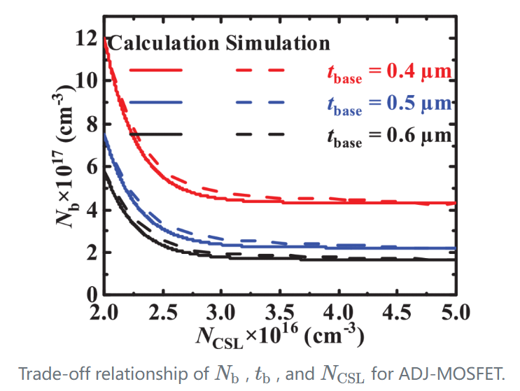
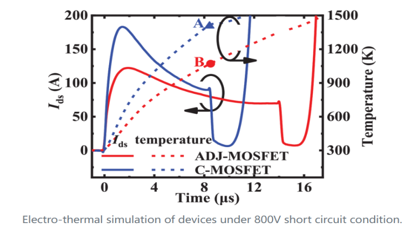
Figure 3: (a) Trade-off relationship of Nb , tb , and Ncsl for ADJ-MOSFET (b) Electro-thermal simulation of devices under 800V short circuit condition.[8]
3.2. Design Methods to Improve Avalanche Reliability
UIS Failure Research and Preliminary Findings
Avalanche failure significantly impacts the reliability of Silicon Carbide Metal-Oxide-Semiconductor Field-Effect Transistors (SiC MOSFETs). Unclamped Inductive Switching (UIS) test experiments have quantitatively demonstrated that the avalanche energy capacity of SiC MOSFETs stands at 1.23 Joules. Simulation analyses accompanying these tests illustrate a progressive increase in the junction temperature of the device throughout the avalanche occurrence. This thermal elevation adversely influences the device's operational stability by decrementing the threshold voltage, which consequently initiates the formation of uncontrolled avalanche currents.
To address this issue and fortify the avalanche resilience of SiC MOSFETs, a novel approach involving the adjustment of the off-state gate voltage is proposed. By strategically lowering this voltage, it is feasible to mitigate the deleterious effects induced by elevated junction temperatures during avalanche conditions. This method not only enhances the overall robustness of the device against avalanche breakdown but also contributes to maintaining stable electrical performance under high-stress conditions. Thus, optimizing the gate voltage settings presents a viable solution for improving the avalanche reliability of SiC MOSFETs, thereby extending their utility in various demanding applications where reliability is critical.

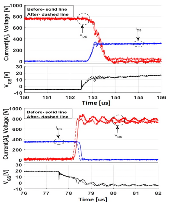
Figure 4: Turn on and turn off of module E during double pulse transient before UIS test and after cutting the bonding wires after UIS tests.[13]
Parasitic Transistor Model and Optimization of P-Well Electric Field Distribution
Within the architecture of Silicon Carbide Metal-Oxide-Semiconductor Field-Effect Transistors (SiC MOSFETs), the phenomenon of avalanche failure is a critical concern impacting device reliability. Recent studies propose that this failure mode can be attributed to the inadvertent activation of an inherent parasitic transistor found within the SiC MOSFET structure. To explore this hypothesis, a detailed parasitic transistor model has been meticulously developed, emphasizing how such activations may precipitate avalanche conditions.
The theoretical underpinnings of this model incorporate an analysis of the series resistance, designated as RB, which is intrinsic to the parasitic transistor's operation. This resistance factor plays a significant role in modulating the behavior of the transistor under stress, influencing the likelihood of avalanche occurrence.
Progressing from theory to application, an advanced SiC MOSFET with enhanced avalanche tolerance was engineered. This enhancement was achieved by carefully optimizing the electric field distribution within the P-well region of the device. The successful fabrication of this high avalanche tolerance device serves to corroborate the theoretical model, confirming the impact of controlled P-well field distribution on mitigating the activation of the parasitic transistor and thereby enhancing the overall robustness of the device against avalanche failures.

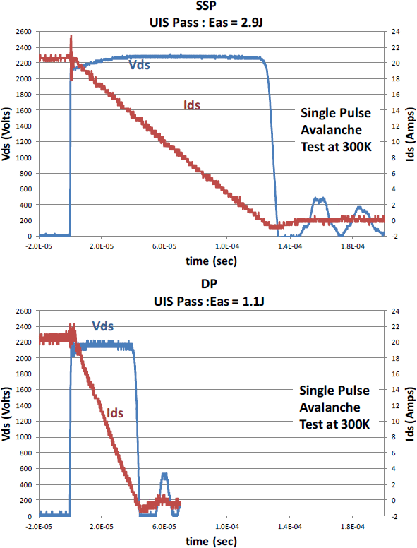
Figure 5: UIS waveforms of SSP (above) and DP (below) designs.[14]
Junction Temperature Research and Failure Mechanism
Through advanced simulation and precise modeling techniques, it was determined that the junction temperature of Silicon Carbide Metal-Oxide-Semiconductor Field-Effect Transistors (SiC MOSFETs) escalates to roughly 937K during avalanche conditions. This temperature coincides with the melting point of aluminum, which is utilized as the surface metallization material in these devices. The correlation between such high temperatures and device failure is substantiated, with localized melting of the surface metal identified as a primary failure mechanism. Additionally, variations inherent in the SiC fabrication process contribute to an uneven distribution of cell current density across the device. This irregularity predisposes the components to thermal accumulation, subsequently precipitating latch-up effects. These phenomena underscore the critical need for uniformity in manufacturing processes to mitigate thermal stress and enhance device reliability under extreme conditions.
Parameter Degradation Research and Structural Optimization
The investigation presented in the study elucidates that Silicon Carbide Metal-Oxide-Semiconductor Field-Effect Transistors (SiC MOSFETs) undergo a notable degradation in on-resistance and an increase in reverse leakage current when subjected to repetitive Unclamped Inductive Switching (UIS) stress. Further detailed analysis indicated that these detrimental effects primarily result from thermal hole injection and subsequent trapping within the gate oxide layer. These phenomena compromise the integrity of the gate oxide, directly impacting the device's performance and reliability under high-stress conditions.
In response to these findings, a novel fabrication strategy was proposed aimed at enhancing the structural resilience and operational stability of SiC MOSFETs. The suggested approach involves the introduction of a thickened gate oxide step layer strategically positioned above the center of the JFET region, as depicted in Figure 5 of the referenced material. By optimizing the thickness and quality of the gate oxide in this manner, the modified structure is expected to exhibit improved resistance to thermal-induced degradation. This enhancement in gate oxide robustness is anticipated to significantly bolster the device's capability to withstand avalanche conditions, thereby extending its functional lifespan and reliability in demanding applications.
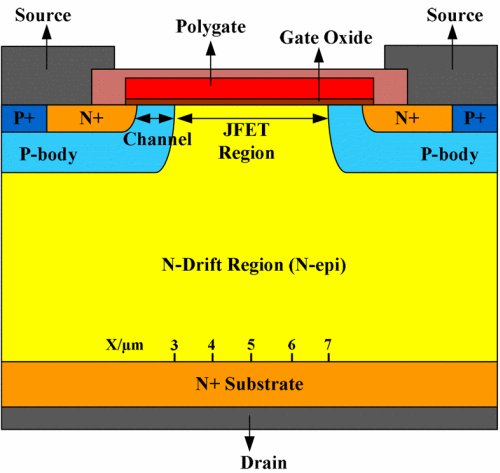
Figure 6: Structure of SiC MOSFET with a thick gate oxide step layer above the center of the JFET region [15]
4. Conclusion
This paper conducts an in-depth study of the mechanisms behind short-circuit and avalanche failures in SiC MOSFETs and proposes a series of innovative design methods that effectively enhance the reliability and stability of these devices. The application of strategies such as integrating AD-JFET regions, reducing off-state gate voltage, and optimizing P-well electric field distribution significantly improves the short-circuit and avalanche tolerance of SiC MOSFETs. These research results provide essential support for the efficient and reliable operation of power electronic equipment, promoting the miniaturization and light-weighting of these devices. Future research will continue to deepen the understanding of SiC MOSFET failure mechanisms and explore more effective reliability enhancement measures to meet the demands of high-voltage, high-power applications.
References
[1]. Kanata T, Nishiwaki K, Hamada K. Development trends of power semiconductors for hybrid vehicles[C]// The 2010 International Power Electronics Conference - ECCE ASIA -. IEEE, 2010.
[2]. Carrasco J M, Franquelo L G, Bialasiewicz J T, et al. Power-Electronic Systems for the Grid Integration of Renewable Energy Sources: A Survey[J]. IEEE Transactions on Industrial Electronics, 2006, 53(4):1002-1016.
[3]. Wang J . A Comparison between Si and SiC MOSFETs[J]. IOP Conference Series Materials Science and Engineering, 2020, 729:012005.
[4]. Goela, J., Brese, N., Burns, L., Pickering, M. (2006). High-Thermal-Conductivity SiC and Applications. In: Shindé, S.L., Goela, J.S. (eds) High Thermal Conductivity Materials. Springer, New York, NY. https://doi.org/10.1007/0-387-25100-6_6.
[5]. Wei R,Sheng S,Yang K,et a1.Thermal Conductivity of 4H-SiC Single Crystals[J].Journal ofApplied Physucs,2013,1 13(5):283.
[6]. J.A.Copper Jr.M.R.Melloch,R.Singh,A.Agarwal,J.W.Palmour. Status and prospects for SiC power MOSFETs[J].IEEE Trans.Electron Devices v01.49,p.658-64,2002.
[7]. A. Elasser and T. P. Chow, "Silicon carbide benefits and advantages for power electronics circuits and systems," in Proceedings of the IEEE, vol. 90, no. 6, pp. 969-986, June 2002, doi: 10.1109/JPROC.2002.1021562.
[8]. L. F. S. Alves et al., "SIC power devices in power electronics: An overview," 2017 Brazilian Power Electronics Conference (COBEP), Juiz de Fora, Brazil, 2017, pp. 1-8, doi: 10.1109/COBEP.2017.8257396.
[9]. M. Zhang, H. Li, Z. Yang, S. Zhao, X. Wang and L. Ding, "Short Circuit Protection of Silicon Carbide MOSFETs: Challenges, Methods, and Prospects," in IEEE Transactions on Power Electronics, vol. 39, no. 10, pp. 13081-13095, Oct. 2024, doi: 10.1109/TPEL.2024.3430897.
[10]. Zhang B, Wang S. A Survey of EMI Research in Power Electronics Systems With WideBandgap Semiconductor Devices[J]. IEEE Journal of Emerging and Selected Topics in Power Electronics, 2019, PP(99):1-1.
[11]. X. Huang, G. Wang, Y. Li, A. Q. Huang and B. J. Baliga, "Short-circuit capability of 1200V SiC MOSFET and JFET for fault protection," 2013 Twenty-Eighth Annual IEEE Applied Power Electronics Conference and Exposition (APEC), Long Beach, CA, USA, 2013, pp. 197-200.
[12]. X. Li et al., "A Novel SiC MOSFET With Embedded Auto-Adjust JFET With Improved Short Circuit Performance," in IEEE Electron Device Letters, vol. 42, no. 12, pp. 1751-1754, Dec. 2021.
[13]. Ionita, Claudiu, Muhammad Nawaz, and Kalle Ilves. "On the short-circuit and avalanche ruggedness reliability assessment of SiC MOSFET modules." Microelectronics Reliability 71 (2017): 6-16.
[14]. Ji I H, Gendron-Hansen A, Lee M, et al. Highly rugged 1200 V 80 mΩ 4-H SiC power MOSFET[C]// International Symposium on Power Semiconductor Devices & Ics. IEEE, 2017.
[15]. S. Liu et al., "Investigations on degradation and optimization of 1.2kV 4H-SiC MOSFET under repetitive unclamped inductive switching stress," 2015 IEEE 27th International Symposium on Power Semiconductor Devices & IC's (ISPSD), Hong Kong, China, 2015, pp. 205-208.
Cite this article
Zhou,G. (2025). Research on the Reliability Methods of SiC MOSFET Power Devices. Applied and Computational Engineering,140,91-99.
Data availability
The datasets used and/or analyzed during the current study will be available from the authors upon reasonable request.
Disclaimer/Publisher's Note
The statements, opinions and data contained in all publications are solely those of the individual author(s) and contributor(s) and not of EWA Publishing and/or the editor(s). EWA Publishing and/or the editor(s) disclaim responsibility for any injury to people or property resulting from any ideas, methods, instructions or products referred to in the content.
About volume
Volume title: Proceedings of the 3rd International Conference on Mechatronics and Smart Systems
© 2024 by the author(s). Licensee EWA Publishing, Oxford, UK. This article is an open access article distributed under the terms and
conditions of the Creative Commons Attribution (CC BY) license. Authors who
publish this series agree to the following terms:
1. Authors retain copyright and grant the series right of first publication with the work simultaneously licensed under a Creative Commons
Attribution License that allows others to share the work with an acknowledgment of the work's authorship and initial publication in this
series.
2. Authors are able to enter into separate, additional contractual arrangements for the non-exclusive distribution of the series's published
version of the work (e.g., post it to an institutional repository or publish it in a book), with an acknowledgment of its initial
publication in this series.
3. Authors are permitted and encouraged to post their work online (e.g., in institutional repositories or on their website) prior to and
during the submission process, as it can lead to productive exchanges, as well as earlier and greater citation of published work (See
Open access policy for details).
References
[1]. Kanata T, Nishiwaki K, Hamada K. Development trends of power semiconductors for hybrid vehicles[C]// The 2010 International Power Electronics Conference - ECCE ASIA -. IEEE, 2010.
[2]. Carrasco J M, Franquelo L G, Bialasiewicz J T, et al. Power-Electronic Systems for the Grid Integration of Renewable Energy Sources: A Survey[J]. IEEE Transactions on Industrial Electronics, 2006, 53(4):1002-1016.
[3]. Wang J . A Comparison between Si and SiC MOSFETs[J]. IOP Conference Series Materials Science and Engineering, 2020, 729:012005.
[4]. Goela, J., Brese, N., Burns, L., Pickering, M. (2006). High-Thermal-Conductivity SiC and Applications. In: Shindé, S.L., Goela, J.S. (eds) High Thermal Conductivity Materials. Springer, New York, NY. https://doi.org/10.1007/0-387-25100-6_6.
[5]. Wei R,Sheng S,Yang K,et a1.Thermal Conductivity of 4H-SiC Single Crystals[J].Journal ofApplied Physucs,2013,1 13(5):283.
[6]. J.A.Copper Jr.M.R.Melloch,R.Singh,A.Agarwal,J.W.Palmour. Status and prospects for SiC power MOSFETs[J].IEEE Trans.Electron Devices v01.49,p.658-64,2002.
[7]. A. Elasser and T. P. Chow, "Silicon carbide benefits and advantages for power electronics circuits and systems," in Proceedings of the IEEE, vol. 90, no. 6, pp. 969-986, June 2002, doi: 10.1109/JPROC.2002.1021562.
[8]. L. F. S. Alves et al., "SIC power devices in power electronics: An overview," 2017 Brazilian Power Electronics Conference (COBEP), Juiz de Fora, Brazil, 2017, pp. 1-8, doi: 10.1109/COBEP.2017.8257396.
[9]. M. Zhang, H. Li, Z. Yang, S. Zhao, X. Wang and L. Ding, "Short Circuit Protection of Silicon Carbide MOSFETs: Challenges, Methods, and Prospects," in IEEE Transactions on Power Electronics, vol. 39, no. 10, pp. 13081-13095, Oct. 2024, doi: 10.1109/TPEL.2024.3430897.
[10]. Zhang B, Wang S. A Survey of EMI Research in Power Electronics Systems With WideBandgap Semiconductor Devices[J]. IEEE Journal of Emerging and Selected Topics in Power Electronics, 2019, PP(99):1-1.
[11]. X. Huang, G. Wang, Y. Li, A. Q. Huang and B. J. Baliga, "Short-circuit capability of 1200V SiC MOSFET and JFET for fault protection," 2013 Twenty-Eighth Annual IEEE Applied Power Electronics Conference and Exposition (APEC), Long Beach, CA, USA, 2013, pp. 197-200.
[12]. X. Li et al., "A Novel SiC MOSFET With Embedded Auto-Adjust JFET With Improved Short Circuit Performance," in IEEE Electron Device Letters, vol. 42, no. 12, pp. 1751-1754, Dec. 2021.
[13]. Ionita, Claudiu, Muhammad Nawaz, and Kalle Ilves. "On the short-circuit and avalanche ruggedness reliability assessment of SiC MOSFET modules." Microelectronics Reliability 71 (2017): 6-16.
[14]. Ji I H, Gendron-Hansen A, Lee M, et al. Highly rugged 1200 V 80 mΩ 4-H SiC power MOSFET[C]// International Symposium on Power Semiconductor Devices & Ics. IEEE, 2017.
[15]. S. Liu et al., "Investigations on degradation and optimization of 1.2kV 4H-SiC MOSFET under repetitive unclamped inductive switching stress," 2015 IEEE 27th International Symposium on Power Semiconductor Devices & IC's (ISPSD), Hong Kong, China, 2015, pp. 205-208.