


1. Introduction
In recent years, a new wide energy gap semiconductor device represented by SiC, with its excellent material properties, has broken through the performance limit of traditional Si-based devices, and has gradually become a research hotspot in the industry [1].
SiC is a compound semiconductor material composed of silicon and carbo, Its energy gap is large (3.2 eV, about 3 times that of silicon-based materials), High breakdown field strength ( about 10 times higher than silicon-based materials ), Large electron saturation migration rate (twice as large as silicon-based materials), High thermal conductivity (3 times higher than silicon-based materials), It has many advantages such as high frequency and high efficiency, high voltage resistance, high temperature resistance, strong radiation resistance and stable chemical properties[2]. Therefore, SiC devices are often used in circuit design to meet the requirements of high frequency and high voltage. SiC MOSEFT is also being used in grid-connected inverters and electronic power transformer, the power device SiC MOSEFT can effectively reduce the power loss of the device, and it is expected that SiC devices will be more widely used in the future power system [3-5].
However, since the SiC drive circuit can work at a higher switching frequency and has a faster switching speed, its electromagnetic interference (EMI) generated in actual operation is more serious than that of the ordinary Si drive circuit. Excessive electromagnetic interference not only makes the equipment unable to pass the corresponding electromagnetic interference standards, but also may have an impact on the control circuit, and may even lead to misoperation of protective equipment. Therefore, in the design of SiC drive circuit, how to reduce the electromagnetic interference in the circuit becomes a problem that cannot be ignored. Power engineers usually use buffering, filtering, resonance and other technologies to solve the electromagnetic compatibility of power products [6,7].
A circuit that is selective to the frequency of a signal is called a filter circuit that enables a signal within a specific frequency range to pass, and prevents a signal outside that frequency range from passing. According to the different passband frequencies, it can be divided into four filtering circuits: low-pass filter (LPF), high-pass filter (HPF), band-pass filter (BPF) and band-stop filter (BEF) [8,9]. In this paper, the EMI generation mechanism of SiC drive circuit is analyzed, and several filtering circuits are proposed to solve the EMI problem in SiC drive circuit.
This paper is divided into three parts: introducing SiC power devices, exploring the principle of electromagnetic interference, and introducing the filter circuit. In the principle part of the filter circuit, the typical structure of the second-order active filter is proposed, and the second-order active low-pass filter circuit and band-stop filter circuit are also introduced.
2. Principle of emi
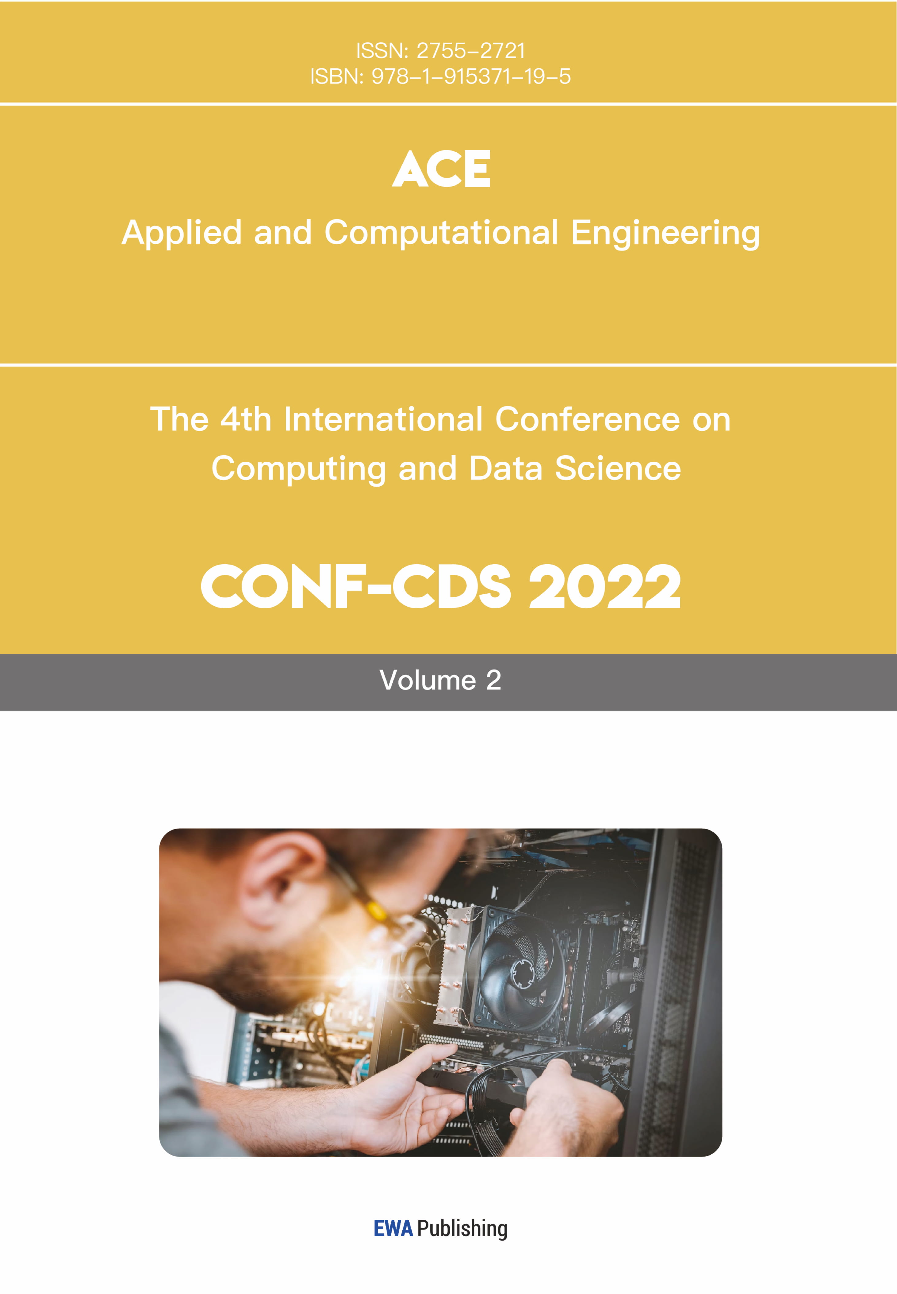
The occurrence of electromagnetic interference must have three basic conditions: the first is the electromagnetic interference source, such as cosmic rays, the external interference generated when the blower works. The second is the path to spread electromagnetic interference energy. The third is the response of the disturbed object. Therefore, electromagnetic interference source, interference propagation coupling path and sensitive decives are called three elements of electromagnetic interference.
|
Figure 1. Three elements of electromagnetic interference. |
According to the different properties of the transmission medium, the transmission of electromagnetic energy from the interference source to the sensitive device has two forms of conduction coupling and radiation coupling. When the electromagnetic interference energy is transmitted along the visible connection circuit between the interference source and the sensitive equipment and the capacitance and mutual inductance between the conductors, the conduction coupling interference is generated. When transmitting outward in the form of electromagnetic waves through space, the radiation coupling interference is generated [10].
Single event Burnout (SEB) refers to the damage mode caused by the impact of neutrons and heavy ions that occasionally enter the ground caused by cosmic rays, which is considered to be the main reason for the accidental failure of high-voltage power components. In particular, compared with the location at 0 m above sea level, the neutron concentration will be as high as more than 10 times, which is prone to problems. Usually, the voltage derating of components and devices with low failure rate is adopted to reduce the risk of accidental failure caused by cosmic rays.
Electromagnetic interference in conducted coupling is usually filtered by filters, such as common-mode inductance in circuit system. Common-mode inductance is also called common-mode choke ring, which is commonly used to filter common-mode electromagnetic interference signals in switching power supply.
3. Circuit Analysis
3.1. Typical structure of second-order active filter
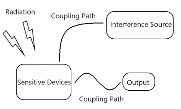
Filter circuits are generally divided into active filter circuits and passive filter circuits, The active filter circuit can make the amplitude frequency characteristic steep. Although the design of passive filter is simple and easy, the amplitude frequency characteristic is not as good as active filter. The actual production is often used to the second-order active filter circuit, the typical structure of the second-order active filter is shown in Fig. 2
|
Figure 2. Typical circuit of second-order active filter. |
X1~X5 are transadmittances, consider Up=Un, according to KCL, the general expression of transfer function can be obtained [11]
\( {G_{(s)}}=\frac{{U_{0}}(s)}{{U_{i}}(s)}=\frac{{A_{uf}}{X_{1}}{X_{4}}}{{X_{5}}({X_{1}}+{X_{2}}+{X_{3}}+{X_{4}})+[{X_{1}}+{X_{2}}(1-{A_{uf}})+{X_{3}}]{X_{4}}} \) (1)
in (1), Auf=1+RF/R1。
3.2. Design of second order active low pass filter
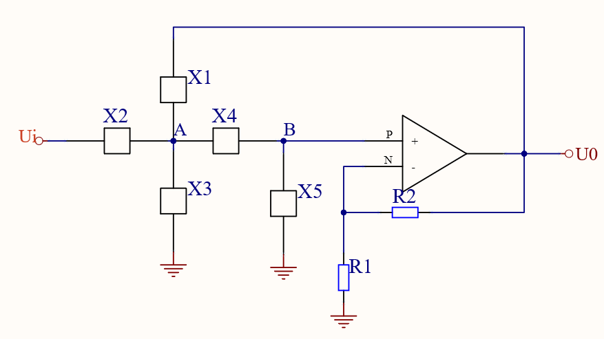
Low-pass filter is suitable for waveform generation circuit, pulse amplification circuit, etc. When designing low-pass filter, its cutoff frequency, quality factors and other parameters are generally considered. The cutoff frequency formula \( {f_{0}}={f_{n}}=\frac{1}{2πRC} \) ,Select the capacitance C1 and C2 values, calculate the resistance values, the second order active low pass filter circuit is shown in Fig. 3.
|
Figure 3. The second order active low pass filter circuit. |
From (1), The transfer function of the voltage-controlled voltage source second-order active low-pass filter is
\( G(s)=\frac{{U_{0}}(s)}{{U_{i}}(s)}=\frac{{G_{0}}ω_{n}^{2}}{{s^{2}}+ξ{ω_{n}}s+ω_{n}^{2}} \) (2)
in (2), \( {ω_{n}} \) is characteristic angular frequency, \( ξ \) is damping coefficient.
The operational amplifier and resistor constitute the voltage-controlled voltage source. The operational amplifier is the in-phase input, which has the advantages of high input resistance and low output resistance. It can provide certain model gain and buffer effect, and is easy to tune. This circuit is widely used in numerical control devices and signal processing circuits. Second-order active low-pass filter filters high frequency noise in the signal, but when the input signal frequency is large, the amplification effect of the circuit is not ideal.
3.3. Active bandstop filter circuit
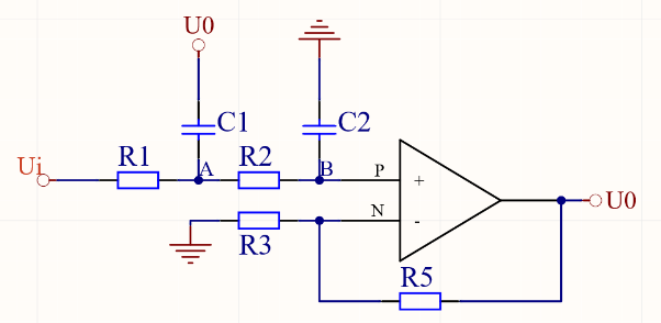
Bandstop filter is suitable for filtering a narrow band frequency in a wide frequency range. It is often used to suppress parasitic passband generated by band pass filter to protect useful signals. If the band-stop filter circuit is paralleled by high-pass filter and low-pass filter, the cut-off frequency of low-pass filter must be lower than that of high-pass filter. The basic second order active bandstop filter circuit is shown in Fig. 4.
|
Figure 4. Active bandstop filter circuit. |
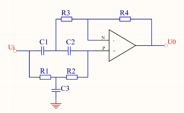
R1, R2, C3 and C1, C2, R3 constitute a dual-T frequency selection network [11]. Using the same phase input, high input resistance, low output resistance, operational amplifier provides amplification and buffering. In the circuit, R1 and R2 is the same as R, C1 and C2 is the same as C, the resistance of R3 is R / 2, the capacitance of C3 between R1 and R2 is 2C. Central Frequency of Bandstop Filter \( {f_{0}}=\frac{1}{2πRC} \) ,when f= \( {f_{0}} \) , the gain is zero, showing the band-stop characteristic [12,13]..
3.4. Driver IC
|
Figure 5. SiC MOSFET driver IC. |
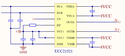
The driver chip is UCC21521 chip from TI Company in the United States, it can meet the requirements of SiC driver. The isolation voltage between input and output reaches up to 1500 V, and the common mode disturbance rejection voltage reaches more than 100 V / ns. The typical value of signal transmission delay is 19 ns, and the current of 4 A can be provided at work.
3.5. SiC Driving Circuit and Bandstop Filter Circuit
The whole circuit is divided into SiC drive circuit and band-stop filter circuit. The active band stop filter circuit adopts a dual-t frequency selection network with adjustable quality factors, which controls the signal in a certain frequency band to receive great attenuation, which makes it almost impossible to pass, while the signals in other frequency ranges can pass smoothly. The bandstop filter circuit is mainly used to eliminate the useless signals of some known frequencies in the drive circuit, so as to reduce the interference to the required signals. A filter circuit is designed to Filter EMI interference, so as to completely filter the signal of a certain frequency band and its second harmonic interference in the output voltage U0.
|
Figure 6. SiC driving circuit and bandstop filter circuit. |
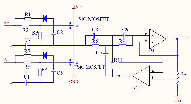
The central frequency of bandstop filter is \( {f_{0}}=\frac{1}{2πRC} \) , for 200Hz power frequency, design stopband center frequency. In circuit design, let C8=C9=0.02μF, then R8=R9 \( ≈ \) 39.8kΩ, C5=0.04μF, then R11 \( ≈ \) 19.9kΩ, if for the 20Hz power frequency, let C8=C9=0.04μF, then R8=R9 \( ≈ \) 199kΩ, C5=0.08μF, then R11 \( ≈ \) 99.5kΩ.
This band-stop filter circuit adds the operational amplifier and potentiometer Rw with feedback function on the basis of the traditional filter circuit, the function of Rw is to adjust the quality factor Q of the circuit. The larger the Q value is, the narrower the stopband width is, and the better the frequency selection characteristics are [14].
4. Conclusion
SiC power electronic devices will play more and more advantages in improving power efficiency and meeting high frequency and high voltage [15,16].. SiC devices will be more widely used in the future. In this paper, the electromagnetic interference of SiC drive circuit is discussed. The second-order active low-pass filter and the second-order active bandstop filter are introduced. The working principle of the filter circuit is studied, and the transfer function is analyzed. Based on the basic second-order active filter circuit, a bandstop filter circuit is proposed in the paper to adjust the frequency selection characteristics according to the resistance value of the potentiometer. The resistance value and capacitance of the bandstop filter circuit are calculated by the bandstop center frequency. The circuit has good filtering, feedback and amplification functions, and has good effect in dealing with the signal interference problems of intermediate frequency signal and low frequency signal.
References
[1]. Weston D. Electromagnetic Compatibility: Principles and Applications, Second Edition, Revised and Expanded[J]. Crc Press, 2001.
[2]. Zhang B, Tang L, Chen T, et al. Application of Third Generation Wide-gap Semiconductor (SiC) Devices in Space Solar Power Station[J]. Space Electronic Technology, 2018.
[3]. Haifu W U, Zhang J, Zhao J, et al. Applications and Challenges of SiC MOSFET in Power System[J]. Journal of Taiyuan University of Technology, 2019.
[4]. Bhattacharya S. Wide-band Gap (WBG) WBG devices enabled MV power converters for utility applications — Opportunities and challenges[C]// Wide Bandgap Power Devices & Applications. IEEE, 2014.
[5]. Huang A Q, Zhu Q, Wang L, et al. 15 kV SiC MOSFET: An enabling technology for medium voltage solid state transformers[J]. CPSS Transactions on Power Electronics and Applications, 2017, 2(2): 118-130.
[6]. Yang D. Design of Driving Circuit for Effective Suppression of Radiated EMI[J]. Microelectronics, 2011.
[7]. Kotny J L, Duquesne T, Idir N. Modeling and design of the EMI filter for DC-DC SiC-converter[C]// 2014.
[8]. Lian-Gang L U. Filter circuits design for filtering 50 Hz power frequency interference[J]. Journal of Liaoning Teachers College (Natural Science Edition), 2012.
[9]. Waters A. Active Filter Design[M]. Macmillan Education, 1991.
[10]. Tu H Y, Lin Y S, Chen P Y, et al. An analysis of the anomalous dip in scattering S22 parameter of InGaP/GaAs heterojunction bipolar transistors (HBTs)[J]. IEEE Transactions on Electron Devices, 1999, 49(10):1831-1833.
[11]. Gui J. Design and Analysis of the Second Order Active Low Pass Filter Circuit[J]. Electronic Science and Technology, 2010.
[12]. Zekai Lyu. Research on High-performance Servodrive and its output filter based on silicon carbide devices. Harbin Institute of Technology,2020.
[13]. Seol H, Park C, Dong H L, et al. A 2.4-GHz HBT power amplifier using an on-chip transformer as an output matching network[C]// Microwave Symposium Digest, 2008 IEEE MTT-S International. IEEE, 2008.
[14]. Li G L, Shu T, Yuan C W, et al. Preliminary investigation on the design and experiment of a spatial filter for dual band high power microwave[J]. Acta Physica Sinica, 2010, 59(12):8591-8596.
[15]. Maloney T J, Dabral S. Novel clamp circuits for IC power supply protection[J]. IEEE Transactions on Components Packaging & Manufacturing Technology Part C, 1995, 19(3):150-161.
[16]. Savary P, Girardot A, Montoriol G, et al. Dual-band multi-mode power amplifier module using a third generation HBT technology[C]// Gallium Arsenide Integrated Circuit (GaAs IC) Symposium, 2001. 23rd Annual Technical Digest. IEEE, 2001.
Cite this article
Liu,Z. (2023). Analysis and research of EMI filter based on SiC power device. Applied and Computational Engineering,4,32-37.
Data availability
The datasets used and/or analyzed during the current study will be available from the authors upon reasonable request.
Disclaimer/Publisher's Note
The statements, opinions and data contained in all publications are solely those of the individual author(s) and contributor(s) and not of EWA Publishing and/or the editor(s). EWA Publishing and/or the editor(s) disclaim responsibility for any injury to people or property resulting from any ideas, methods, instructions or products referred to in the content.
About volume
Volume title: Proceedings of the 3rd International Conference on Signal Processing and Machine Learning
© 2024 by the author(s). Licensee EWA Publishing, Oxford, UK. This article is an open access article distributed under the terms and
conditions of the Creative Commons Attribution (CC BY) license. Authors who
publish this series agree to the following terms:
1. Authors retain copyright and grant the series right of first publication with the work simultaneously licensed under a Creative Commons
Attribution License that allows others to share the work with an acknowledgment of the work's authorship and initial publication in this
series.
2. Authors are able to enter into separate, additional contractual arrangements for the non-exclusive distribution of the series's published
version of the work (e.g., post it to an institutional repository or publish it in a book), with an acknowledgment of its initial
publication in this series.
3. Authors are permitted and encouraged to post their work online (e.g., in institutional repositories or on their website) prior to and
during the submission process, as it can lead to productive exchanges, as well as earlier and greater citation of published work (See
Open access policy for details).
References
[1]. Weston D. Electromagnetic Compatibility: Principles and Applications, Second Edition, Revised and Expanded[J]. Crc Press, 2001.
[2]. Zhang B, Tang L, Chen T, et al. Application of Third Generation Wide-gap Semiconductor (SiC) Devices in Space Solar Power Station[J]. Space Electronic Technology, 2018.
[3]. Haifu W U, Zhang J, Zhao J, et al. Applications and Challenges of SiC MOSFET in Power System[J]. Journal of Taiyuan University of Technology, 2019.
[4]. Bhattacharya S. Wide-band Gap (WBG) WBG devices enabled MV power converters for utility applications — Opportunities and challenges[C]// Wide Bandgap Power Devices & Applications. IEEE, 2014.
[5]. Huang A Q, Zhu Q, Wang L, et al. 15 kV SiC MOSFET: An enabling technology for medium voltage solid state transformers[J]. CPSS Transactions on Power Electronics and Applications, 2017, 2(2): 118-130.
[6]. Yang D. Design of Driving Circuit for Effective Suppression of Radiated EMI[J]. Microelectronics, 2011.
[7]. Kotny J L, Duquesne T, Idir N. Modeling and design of the EMI filter for DC-DC SiC-converter[C]// 2014.
[8]. Lian-Gang L U. Filter circuits design for filtering 50 Hz power frequency interference[J]. Journal of Liaoning Teachers College (Natural Science Edition), 2012.
[9]. Waters A. Active Filter Design[M]. Macmillan Education, 1991.
[10]. Tu H Y, Lin Y S, Chen P Y, et al. An analysis of the anomalous dip in scattering S22 parameter of InGaP/GaAs heterojunction bipolar transistors (HBTs)[J]. IEEE Transactions on Electron Devices, 1999, 49(10):1831-1833.
[11]. Gui J. Design and Analysis of the Second Order Active Low Pass Filter Circuit[J]. Electronic Science and Technology, 2010.
[12]. Zekai Lyu. Research on High-performance Servodrive and its output filter based on silicon carbide devices. Harbin Institute of Technology,2020.
[13]. Seol H, Park C, Dong H L, et al. A 2.4-GHz HBT power amplifier using an on-chip transformer as an output matching network[C]// Microwave Symposium Digest, 2008 IEEE MTT-S International. IEEE, 2008.
[14]. Li G L, Shu T, Yuan C W, et al. Preliminary investigation on the design and experiment of a spatial filter for dual band high power microwave[J]. Acta Physica Sinica, 2010, 59(12):8591-8596.
[15]. Maloney T J, Dabral S. Novel clamp circuits for IC power supply protection[J]. IEEE Transactions on Components Packaging & Manufacturing Technology Part C, 1995, 19(3):150-161.
[16]. Savary P, Girardot A, Montoriol G, et al. Dual-band multi-mode power amplifier module using a third generation HBT technology[C]// Gallium Arsenide Integrated Circuit (GaAs IC) Symposium, 2001. 23rd Annual Technical Digest. IEEE, 2001.