


1. Introduction
Electronic design automation (EDA), also known as electronic computer-aided design (ECAD), is a way of using computer software to design, test, or aid the design process of intergraded circuits. The goal was to help engineers produce faster and more reliable chip through computer software while meeting the time of marking each year. In the past few decades, the field of intergraded circuits has evolved rapidly. Die size has grown over twice the size every 10 years and the clock frequency has doubled every two years. According to Moore’s law the transistor size inside the chip is shrinking by roughly 7% every single year. This has been a consistent trend for decades and the industry is doing its best to follow it. However, this trend predicted by Gordon Moore has been slowing down with every shrinking size of the transistor. We are getting closer to the physical limit of the device and the term size of the transistor which originally refer to the physical length of the gate has lost its meaning around 45 nm. Therefore, in order to further improve our chip, we are tasked with further improving the complexity of the design. One way of achieving this is to increase the transistor count. The drawback is that the chip would consume more power, and the size of the chip would also increase. To counter these drawbacks new design becomes more complex than ever, and they require teams of engineer month to produce a reliable product. This could potentially be an issue for companies that want to maximize their profit, since a slight delay to market could lead to a huge difference in final sales. This is where EDA comes in. We will first explain the background of EDA and how it has evolved over the years. Then we will further discuss how ML could be applied to traditional EDA tools to drastically reduce the time required for some of the trickier design processes. We will finish with a look into the future of electronic design automation which will include its potential and risks.
2. EDA background
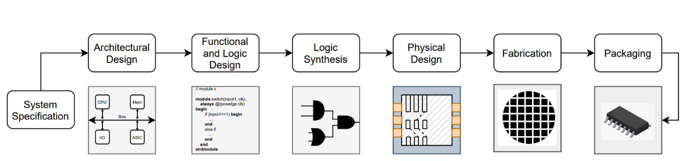
Electronic design automation is the process of using a collection of computer software to help engineers design electronic products. It started as a subarea in computer aiding design (CAD) tools which was originated in the 1960s to help engineers analyze circuit layouts [1]. Since then, different kinds of EDA tools have emerged to help designers in different area of the process. The modern chip design process starts with system specification and architectural design. This will create a library of standard modules such as NAND gates, OR, and XOR gates. This standard cell library would help the designer focus on higher-level design in the future without considering individual cells. Then the designers can move on to logic design and logic synthesis. Design capture tools, also called schematic editors, are created to help capture the schematic of the circuit and aid engineering in this logic design process. An example of this is the Verilog language, which is able to capture the behavior of the circuit in code form and generate a simulation for the logic. A physical design layout is required in order to be able to manufacture the actual circuit. Four main steps are needed in this area: “floorplanning, placement, clock insertion, and routing” [1]. Floorplanning considers the geometric constraints of the IC and places the RTL component in a suitable region of the layout. The placement step places all the logic gates in the correct location. Clock insertion and routing connect all the components and the clock via wires. Layout and synthesis tools are provided to engineers to transform their finished schematics into physical layouts, which allows this process to be a lot more time-efficient [2]. The above EDAs were created to help engineers design circuits, but with the help of machine learning, it is also possible to use artificial intelligence to design the entire integrated circuit. Many major tech companies are already using their existing AI technology to explore the possibility of replacing human designers with AI, and most of them have already seen promising results. Nvidia claims that their AI is capable of creating chips with minor helps from engineers in some more complex areas [3]. Recently, Google stated that their artificial intelligence is capable of designing computer chips better than humans [4].
|
Figure 1. IC design glow. [1] |
3. Machine learning applications in EDA
In this section, we will be looking at how machine learning is implemented in electronic design automation.
3.1. Placement
Chip macro placement can be a very time-consuming process compared to other areas of chip design. At this stage, each gate must be mapped to the exact location in the layout to maximize the IC performance. The design is optimized by lowering the wire length and density while increasing the circuit speed. The state of the art none machine learning algorithm is analytical placement [5]. It consists of global placement, where we lower the constraints, making the problem easier to solve, legalization which recovers the constraints that we ignored, and detailed placement, which optimizes the solution that was acquired. Modern ICs have become a lot denser within similar sizes to maximize the increased demand for performance and the layout placement process becomes even more complicated with this increase in density of the design. This section will introduce several implementations of ML in placement that helps increase the speed of the process.
The first method, provided by Budak, A. F. et al [6], focuses on the macro placement improvement of the circuit. It uses reinforcement learning that sees locations as variables and utilizes an objective function to determine the performance of the result layout. Several constraints are also introduced to make sure that the chip still obeys the standard rules of circuit design. This turns the placement problem into an optimization problem which is applicable for RL. The method starts by placing the macros in the circuit individually. After placing all the macros, the reward function is called to determine the performance. Then it uses a policy-based method to change the parameters and repeat this training process, so it keeps improving.
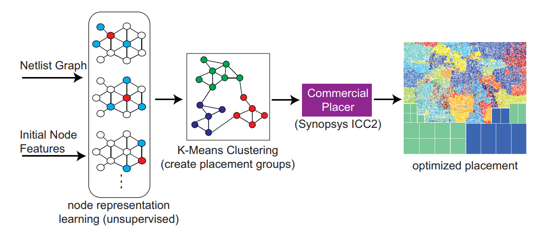
Another method introduced by Lu, Y. C. et al [7] offered to improve VLSI placement using a GNN that the authors called PL-GNN. The process starts with an unsupervised node representation learning which takes an undirected clique-based graph, transformed from the original VLSI netlist’s directed hypergraphs, and uses a variation of GNN called GraphSAGE to perform the learning and obtain the node representation. Then the author uses the weighted K-means clustering algorithm [8] to scatter the original design into clusters of placement groups. Finally, the cluster group is put into a commercial placer to get the final layout design. The result of this method is an improvement by “3.9% in wirelength, 2.8% in power, and 85.7% in worst negative slack reduction” [7] which is a very promising result.
|
Figure 2. PL-GNN process flow. [7] |
3.2. Routing
In this section we will show some machine learning applications regarding routing. This step takes all the placed components and wires them together. Additionally, all the switches need to be tested after the routing to make sure all the connections are working. This is another very time-consuming process and is categorized as an NP-hard or NP-complete problem. Machine learning is able to provide earlier estimations to speed up the routing process.
In “Reinforcement Learning for Electronic Design Automation: Case Studies and Perspectives: (Invited Paper)” [6], a typical method of using an and-invertor graph (AIG) and perform graph optimization, is solved using reinforcement learning. Here, after the logic is turned into an AIG, one of five optimizations is chosen: “balance, rewrite, refactor, rewrite with zero-cost replacement, and refactor with zero-cost replacement” [6]. The reward for the training process is calculated by comparing the input and output nodes and logic depth. With enough training the RL method would outperform the traditional method.
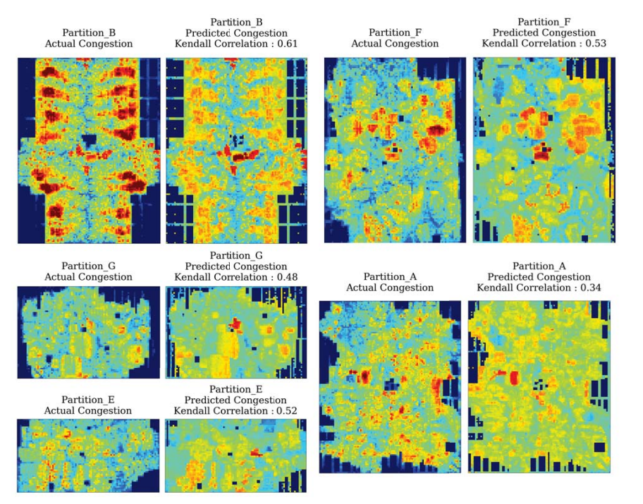
Machine learning can also be applied to predict routing congestion. A routing congesting is where an area has too many wires inside that it becomes congested, which hinders the performance of the device. In [9], the author employed a graph attention network that takes a simple undirected graph of the circuit netlist. The cells of the circuit are treated as nodes, and the edge suggests that the cells are connected. The nodes are also embedded with the corresponding cell features, for example logic and size. Using this network, the author was able to detect almost all the routing congestion in the given tests. The results of this congestion prediction are presented in Figure 3.
|
Figure 3. Actual Congestion vs Predicted Congestion. [9] |
3.3. Data measuring
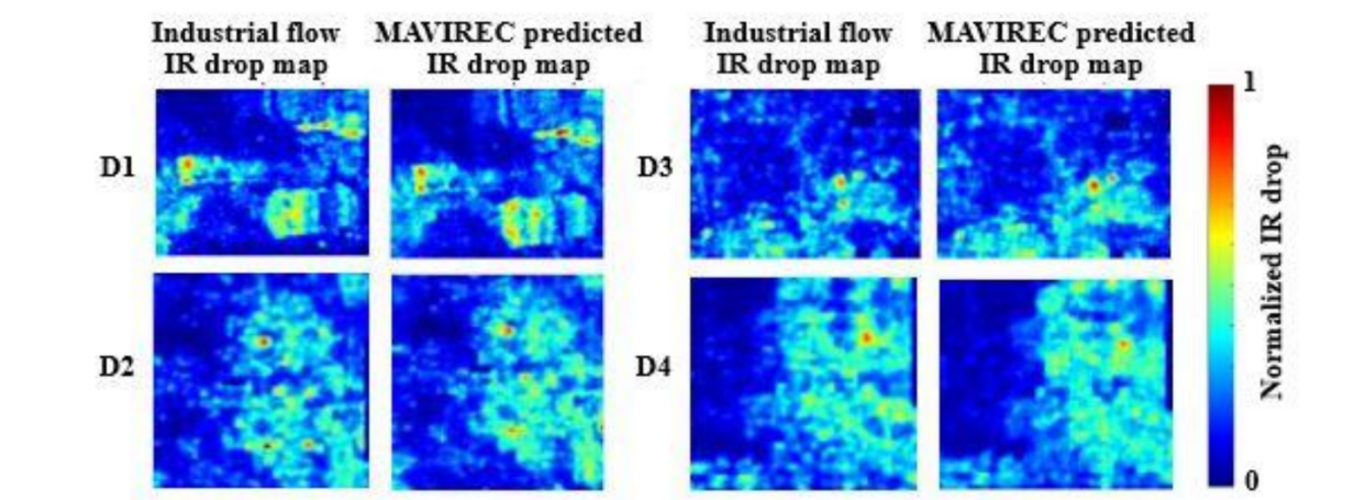
Machine learning is also used in data measuring that is essential for IC optimization. In "MAVIREC: ML-Aided Vectored IR-Drop Estimation and Classification," [10], the team at Nvidia uses EDA to better estimate the IR drop and parasitics during the process of design. The IR drop is the electrical potential difference between the input and output during current flow. Traditionally, this would require an engineer to run a power simulation on the design, and the process using a non-machine learning CAD tool takes roughly 3 hours. However, since the acceptable specs of IR drop were already provided prior to the design, a machine learning network called the u-net can be implemented to drastically reduce the time. A u-network, originally created for biomedical image segmentation, is basically a convolutional neural network with a bottle neck concatenation section in the middle between the encoder section and the decoder section [11]. This machine learning network would take in power map input and convert it into an IR drop map output using semantic segmentation. The entire process takes around 18 minutes, which is a substantial improvement from the traditional method. The acquisition of the input power map can also be optimized via a graph neural network to estimate how often each node in the IC changes, which would give us a very accurate estimated power map with very little time compared to traditional methods.
|
Figure 4. Actual IR drop map vs predicted IR drop map. |
Parasitic prediction is another area that can be accelerated with artificial intelligence. Parasitic, for example, parasitic capacitance, is created when electrical components are too close to each other, creating an unwanted element between them that is not there by design. This can create unnecessary connections between components and hinder the performance of the circuit. Since the size of the IC is shrinking by roughly 7% every year, the gaps between components are getting smaller. Thus, it is important to know where these parasitics are, so we can either change the design or introduce dielectric material between the gaps to reduce the electron flow. Traditionally, this would require the layout designer to extract the parasitic from the planar schematic provided by the circuit designers, and the result would be sent back to the circuit designer for further improvement. This means that the circuit and layout designers would have to iterate through this design process repeatedly since the circuit designer would not be able to know the effect of the changes on the parasitic without the feedback of the layout designer. This creates a very repetitive and labor-intensive revision process. A technique proposed by Ren, H., Kokai el at [12] eliminates this problem by predicting the parasitics with only the circuit schematics before the layout design. They used a graphical neural network they called ParaGraph that map each component (resistor, transistor…) into nodes including net nodes and outputs the net parasitics and the device parasitics. This gives a very accurate prediction before even starting the layout design and reduces the workload created by unnecessary iterative testing.
4. Future
In this section we will look into some of the advantages of EDA, its challenges and how it might develop in the future.
4.1. Benefits
4.1.1. Reduce workload and time. As we can see in previous examples, the most significant improvement for ML in EDA is how it can save time and work for the designer. For example, the parasitic prediction method introduced by Ren, H., Kokai el at [12] was able to reduce the process of multiple circuit revisions by providing a very accurate prediction prior to the layout design process. The U-net IR prediction method [10] was capable of cutting the time of the process from its original 3 hours to around 18 minutes. Clearly, when it comes to efficiency, machine learning is proven to be far superior than traditional methods. With further investment in all areas of the design process, we may see an even bigger jump in performance in chip design.
4.1.2. Existing resources. The field of machine learning is already well developed in some of the other areas. In a lot of the examples in this paper, the actual machine learning methods are implemented using some modification or combination of existing knowledge. In some cases, for example the RL routing method [6], we see a trend of converting electrical design problems into machine learning problems via graph theory. This is a really good starting point for researcher who have existing knowledge in machine learning or those who have experience in machine learning implementation in other areas. This also opens up opportunities for collaboration between the electronic design community and the machine learning community.
4.2. Threats
4.2.1. Vulnerable to attacks. According to K. Liu el at [13], one of the major concerns of utilizing deep learning in EDA is its potential to be vulnerable to malicious attacks. This is mainly due to the nature of the vulnerability of DL and has been well acknowledged by the ML community. The two attacks that the author introduced [13] are adversarial perturbation attacks and backdooring attacks. Adversarial perturbation attacks allow the attacker to fool the DNN based detectors by manually introducing what the detector was looking for to get a false detection. Backdooring attack requires the attacker to gain access to the training dataset of the DNN and modify it so that the supposed to be detected data is ‘hided’ from the DNN. This will result in the trained detector being incapable of detecting the hidden hotspot and allow the attacker to pass through the DNN network when they are not supposed to.
4.2.2. High cost on materials. This is a potential issue for people with a limited amount of resources. The author in [6] suggests that the existing EDA tools, which are essential for evaluating the reward function, can have quite an expensive license fee. This can be a problem for those who are not working with existing EDA tools. However, most people who are working in IC design already have access to a number of EDA tools for their daily design. For them, starting research in ML implantation may not be as costly since the license fee already exists in their day-to-day work. For those who do not have access to EDA tools, a collaboration with an active IC designer with access to EDA could be a potential solution. This is also one of the benefits of the collaboration between the electronic design community and the machine learning community discussed in the previous paragraph.
4.3. Opportunities
As discussed in the EDA background, the current trajectory of EDA tools is shifting from improving part of the design process to helping engineers design the entire thing. In 2021, researchers from Google (Mirhoseini et al) [4] claimed that their ML method is capable of solving the entire floorplanning problem in under six hours and that the result floorplan is superior or comparable to their human designed counterparts. If more of this design AI is introduced to the market for all the other design processes, this could essentially replace humans as chip designers and help save thousands of hours of workload. However, due to the native vulnerability of ML, researchers need to make sure that the new generation of EDA tools are well protected. This would require more money and resources for both the ML application and cybersecurity research, which could be a problem for those who lack sufficient funding.
5. Conclusion
This paper gives a rough introduction to the machine learning implementations in electrical design automation. We conclude that though machine learning implementations can have some potential issues, many of them have their remedies and that the benefit of using machine learning in EDA significantly outweighs the risk that it carries. Unfortunately, this paper wasn’t able to cover ML in all the processes of the IC. We will be researching further into the field of ML in EDA and getting a broader understanding of how it is implemented. As circuit complexity keeps increasing, traditional EDA tools are slowly losing their magic. Machine learning has been transformational for the area of electrical design automation and has become an important part of the new generation of electrical design tools. We hope that this paper gives a good introduction to people who are looking into the field of machine learning in electrical design automation and provides some starting points in their future research.
References
[1]. Lopera, D. S., Servadei, L., Kiprit, G. N., Hazra, S., Wille, R., & Ecker, W. (2021). A Survey of Graph Neural Networks for Electronic Design Automation. 2021 ACM/IEEE 3rd Workshop on Machine Learning for CAD (MLCAD), Machine Learning for CAD (MLCAD), 2021 ACM/IEEE 3rd Workshop On, 1–6.
[2]. D., S. A. (2021). Electronic Design Automation Tools: A Review. IUP Journal of Electrical & Electronics Engineering, 14(4), 27–32.
[3]. NVIDIA. (2022). Insights from NVIDIA Research. Retrieved from https://www.nvidia.com/en-us/on-demand/session/gtcspring22-s42013/?ncid=afm-chs-44270&ranMID=44270&ranEAID=kXQk6%2AivFEQ&ranSiteID=kXQk6.ivFEQ-jNcbNKs0ktck5rPkTF4B.Q.
[4]. Mirhoseini, A., Goldie, A., Yazgan, M. et al. (2021). A graph placement methodology for fast chip design. Nature 594, 207–212.
[5]. C.-K. Cheng, A. B. Kahng, I. Kang, and L. Wang, “RePlAce: Advancing solution quality and routability validation in global placement,” IEEE Transactions on Computer-Aided Design of Integrated Circuits and Systems, vol. 38, no. 9, pp. 1717–1730, 2019.
[6]. Budak, A. F., Jiang, Z., Zhu, K., Mirhoseini, A., Goldie, A., & Pan, D. Z. (2022). Reinforcement Learning for Electronic Design Automation: Case Studies and Perspectives: (Invited Paper). 2022 27th Asia and South Pacific Design Automation Conference (ASP-DAC), Design Automation Conference (ASP-DAC), 2022 27th Asia and South Pacific, 500–505.
[7]. Lu, Y. C., Pentapati, S., & Lim, S. K. (2020). Vlsi placement optimization using graph neural networks. In 34th Advances in Neural Information Processing Systems (NeurIPS) Workshop on ML for Systems.
[8]. De Amorim, R. C., & Mirkin, B. (2012). Minkowski metric, feature weighting and anomalous cluster initializing in K-Means clustering. Pattern Recognition, 45(3), 1061-1075.
[9]. Kirby, R., Godil, S., Roy, R., & Catanzaro, B. (2019). Congestionnet: Routing congestion prediction using deep graph neural networks. In 2019 IFIP/IEEE 27th International Conference on Very Large Scale Integration (VLSI-SoC) (pp. 217-222). IEEE.
[10]. V. A. Chhabria, Y. Zhang, H. Ren, B. Keller, B. Khailany and S. S. Sapatnekar. (2021). "MAVIREC: ML-Aided Vectored IR-Drop Estimation and Classification," 2021 Design, Automation & Test in Europe Conference & Exhibition (DATE), pp. 1825-1828.
[11]. Ronneberger, O., Fischer, P., & Brox, T. (2015). U-net: Convolutional networks for biomedical image segmentation. In International Conference on Medical image computing and computer-assisted intervention (pp. 234-241). Springer, Cham.
[12]. Ren, H., Kokai, G. F., Turner, W. J., & Ku, T. S. (2020). ParaGraph: Layout parasitics and device parameter prediction using graph neural networks. In 2020 57th ACM/IEEE Design Automation Conference (DAC) (pp. 1-6). IEEE.
[13]. K. Liu, J. J. Zhang, B. Tan and D. Feng. (2021). "Can We Trust Machine Learning for Electronic Design Automation?," 2021 IEEE 34th International System-on-Chip Conference (SOCC), pp. 135-140.
Cite this article
Tian,Z. (2023). Introduction to machine leaning in electronic design automation (EDA). Applied and Computational Engineering,6,415-421.
Data availability
The datasets used and/or analyzed during the current study will be available from the authors upon reasonable request.
Disclaimer/Publisher's Note
The statements, opinions and data contained in all publications are solely those of the individual author(s) and contributor(s) and not of EWA Publishing and/or the editor(s). EWA Publishing and/or the editor(s) disclaim responsibility for any injury to people or property resulting from any ideas, methods, instructions or products referred to in the content.
About volume
Volume title: Proceedings of the 3rd International Conference on Signal Processing and Machine Learning
© 2024 by the author(s). Licensee EWA Publishing, Oxford, UK. This article is an open access article distributed under the terms and
conditions of the Creative Commons Attribution (CC BY) license. Authors who
publish this series agree to the following terms:
1. Authors retain copyright and grant the series right of first publication with the work simultaneously licensed under a Creative Commons
Attribution License that allows others to share the work with an acknowledgment of the work's authorship and initial publication in this
series.
2. Authors are able to enter into separate, additional contractual arrangements for the non-exclusive distribution of the series's published
version of the work (e.g., post it to an institutional repository or publish it in a book), with an acknowledgment of its initial
publication in this series.
3. Authors are permitted and encouraged to post their work online (e.g., in institutional repositories or on their website) prior to and
during the submission process, as it can lead to productive exchanges, as well as earlier and greater citation of published work (See
Open access policy for details).
References
[1]. Lopera, D. S., Servadei, L., Kiprit, G. N., Hazra, S., Wille, R., & Ecker, W. (2021). A Survey of Graph Neural Networks for Electronic Design Automation. 2021 ACM/IEEE 3rd Workshop on Machine Learning for CAD (MLCAD), Machine Learning for CAD (MLCAD), 2021 ACM/IEEE 3rd Workshop On, 1–6.
[2]. D., S. A. (2021). Electronic Design Automation Tools: A Review. IUP Journal of Electrical & Electronics Engineering, 14(4), 27–32.
[3]. NVIDIA. (2022). Insights from NVIDIA Research. Retrieved from https://www.nvidia.com/en-us/on-demand/session/gtcspring22-s42013/?ncid=afm-chs-44270&ranMID=44270&ranEAID=kXQk6%2AivFEQ&ranSiteID=kXQk6.ivFEQ-jNcbNKs0ktck5rPkTF4B.Q.
[4]. Mirhoseini, A., Goldie, A., Yazgan, M. et al. (2021). A graph placement methodology for fast chip design. Nature 594, 207–212.
[5]. C.-K. Cheng, A. B. Kahng, I. Kang, and L. Wang, “RePlAce: Advancing solution quality and routability validation in global placement,” IEEE Transactions on Computer-Aided Design of Integrated Circuits and Systems, vol. 38, no. 9, pp. 1717–1730, 2019.
[6]. Budak, A. F., Jiang, Z., Zhu, K., Mirhoseini, A., Goldie, A., & Pan, D. Z. (2022). Reinforcement Learning for Electronic Design Automation: Case Studies and Perspectives: (Invited Paper). 2022 27th Asia and South Pacific Design Automation Conference (ASP-DAC), Design Automation Conference (ASP-DAC), 2022 27th Asia and South Pacific, 500–505.
[7]. Lu, Y. C., Pentapati, S., & Lim, S. K. (2020). Vlsi placement optimization using graph neural networks. In 34th Advances in Neural Information Processing Systems (NeurIPS) Workshop on ML for Systems.
[8]. De Amorim, R. C., & Mirkin, B. (2012). Minkowski metric, feature weighting and anomalous cluster initializing in K-Means clustering. Pattern Recognition, 45(3), 1061-1075.
[9]. Kirby, R., Godil, S., Roy, R., & Catanzaro, B. (2019). Congestionnet: Routing congestion prediction using deep graph neural networks. In 2019 IFIP/IEEE 27th International Conference on Very Large Scale Integration (VLSI-SoC) (pp. 217-222). IEEE.
[10]. V. A. Chhabria, Y. Zhang, H. Ren, B. Keller, B. Khailany and S. S. Sapatnekar. (2021). "MAVIREC: ML-Aided Vectored IR-Drop Estimation and Classification," 2021 Design, Automation & Test in Europe Conference & Exhibition (DATE), pp. 1825-1828.
[11]. Ronneberger, O., Fischer, P., & Brox, T. (2015). U-net: Convolutional networks for biomedical image segmentation. In International Conference on Medical image computing and computer-assisted intervention (pp. 234-241). Springer, Cham.
[12]. Ren, H., Kokai, G. F., Turner, W. J., & Ku, T. S. (2020). ParaGraph: Layout parasitics and device parameter prediction using graph neural networks. In 2020 57th ACM/IEEE Design Automation Conference (DAC) (pp. 1-6). IEEE.
[13]. K. Liu, J. J. Zhang, B. Tan and D. Feng. (2021). "Can We Trust Machine Learning for Electronic Design Automation?," 2021 IEEE 34th International System-on-Chip Conference (SOCC), pp. 135-140.