


1. Introduction
With today's industrialization, people's dependence on energy is increasing. Currently, with national policies such as carbon peaking, clean energy has become an integral part of social development. Solar energy, as a kind of clean energy, is gradually becoming a powerful alternative to traditional fossil energy. In 1954, the U.S. Bell Laboratories for the first time made monocrystalline silicon solar cells, photovoltaic power generation began to move towards the stage of history; in the 1970s, the second generation of solar cells, represented by CdTe, GaAs and CIGS, further developed solar cells with its cost advantages and performance optimization; up to now, there are new breakthroughs in solar cells, and chalcogenide solar cells (PVSKs) with simple preparation process and high photovoltaic conversion efficiency are widely used in photovoltaic, LED and other fields. Although there are many groups to carry out in-depth research on chalcogenide solar cells, which promotes the rapid development of chalcogenide solar cells [1], there is still no summary of optimization ideas about the structure of each layer. In this paper, based on the layered structure of chalcogenide solar cells, we summarize the research progress of chalcogenide solar cell efficiency enhancement in recent years, and put forward optimization schemes from the device point of view, such as doping ions, and adding Lewis acids and bases. Finally we point out the possibility of realizing large-size preparation and further efficiency improvement of chalcogenide solar cells in the future. This paper is a guide for the further modification and development of chalcogenide solar cells.
2. Principle of trans-calcite solar cells
2.1. Structure of calcitonite solar cells
The structure of a typical trans-type chalcogenide solar cell is shown in Fig. 1, from bottom to top: Transparent Conductive Oxide layer (Transparent Conductive Oxide), Hole Transport Layer (Hole Transport Layer), Chalcogenide Light Absorption Layer (Perovskite), Electron Transport Layer), Metal Electrode (Metal).
(1) Transparent Conductive Oxide Layer: This layer serves as the anode of the battery as the sunlight incident surface. The role of this layer is to transmit the sunlight and transfer it to the internal battery while transferring the current, so it needs high light transmission rate and good conductivity, and is generally made by using Indium Tin Oxide (ITO) or Fibrous Tin Oxide (FTO) as the raw material.
(2) Hole Transport Layer (HTL): It acts as a channel for hole transport and prevents electron transport at the same time. Materials such as nickel oxide [2] or cuprous compounds [3] can be used as the hole transport layer, but currently PTAA, PEDOT:PSS, and Sprio-OMeTAD are more commonly used as the hole transport layer in trans-calcitonite solar cells [3].
(3) Chalcogenide layer: chalcogenide is an ionic crystal with the chemical formula ABX3, and the crystal structure is shown in Fig. 2, where A stands for CH3NH3+, CH(NH2)2+, or Cs+, B stands for Pb+ or Sn2+, and X is generally a halogen ion, such as I-, Br-, or Cl-. Chalcogenide layer mainly plays the role of light absorption and conversion, which has been heavily researched is the lead-based chalcogenide, the current single-junction cell with its chalcogenide layer has reached a maximum efficiency of 26.50%, but its shortcomings are also very obvious, the presence of lead element has potential harm to the environment and human safety, so many groups focus on the research of lead-free chalcogenide, such as tin-based chalcogenide solar cells (PVSKs) and have achieved some results, the current efficiency can reach 15.7%.
(4) electron transport layer ETL: as a channel for electron transport and at the same time prevent the transport of holes. n-type semiconductor electron transport layer can be prepared from a variety of materials, including inorganic materials such as TiO2, SnO2, ZnO, etc., organic materials can be used C60, BCP, etc. Now more often used is TiO2 as the electron transport layer. TiO2 layer consists of dense TiO2 and mesoporous TiO2 two layers of material, which, dense TiO2 is used to prevent the conductive base and chalcogenide direct contact, to avoid the hole to the conductive substrate transmission; mesoporous TiO2 for the growth of chalcogenide to provide support for the formation of a hybrid layer for the transmission of electrons.
(5) Metal electrodes: Metal electrodes generally use common conductive materials such as gold, silver, and copper as the cathode of the chalcogenide solar cell.
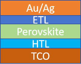
Figure 1: Structure of trans-calcitonite
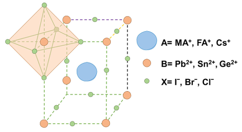
Figure 2: Structure of chalcogenide
2.2. Principle of operation of trans-calcitonite solar cells
When the sunlight irradiation to the transparent conductive oxide layer, photons in the energy higher than the width of the forbidden band of chalcogenide part (hv>Eg) will be absorbed by the chalcogenide, excitation of chalcogenide in the valence band of the electrons. Electrons from the valence band away from the conduction band to reach the point of the formation of holes in the valence band. So that the resulting electron-hole pairs are called excitons. Under the action of thermal energy, the exciton changes into free electrons and free holes, at this time the Fermi energy level of chalcocite from unity to split the electron Fermi energy level Efn and hole Fermi energy level Efp,. At this time, the electron transport layer material Fermi energy level is lower than that of the chalcocite Efn, the hole transport layer material Fermi energy level is higher than that of the chalcocite Efp. At this time, the directional movement of the electrons and holes occur, and each of them flows to itself from the chalcocite layer. chalcogenide layer to their own transport layer, and finally to the electrode, which turns on the external circuit circuit, forming a loop and generating an electric current [4, 5].
3. Advances in the optimization of trans-calcium titanic cells
Optimization of the efficiency and other aspects of the chalcogenide battery has always been the goal of researchers relentlessly pursued [6]. At present, various research groups mainly focus on the optimization of chalcogenide absorption layer [7, 8], electron transport layer [9] and hole transport layer [10], and constantly put forward new optimization ideas.
3.1. Development of calcite light absorbing layers
Recent advancements in optimizing chalcogenide light-absorbing layers have focused on interfacial engineering, precursor stoichiometry control, and crystallization modulation. A prominent strategy involves the use of organic additives to passivate surface defects [11]. For instance, Zhang et al. [12] incorporated a zwitterionic molecule (PEA-Br) at the chalcogenide interface. The Br⁻ ions effectively passivated halide vacancies, while the bulky PEA⁺ cations suppressed ion migration. This dual functionality enhanced charge extraction and stability, yielding a 22.3% PCE compared to 19.1% for untreated devices, with 90% efficiency retention after 1,000 hours under continuous illumination.
Precursor engineering has also proven critical for optimizing film quality. Lee et al. [13] demonstrated that tuning the PbCl₂ : MAI molar ratio during solution processing reduced pinhole density and improved crystallite orientation. Films with a 1:3 ratio exhibited a 300 nm grain size and a 21.5% PCE, outperforming the 18.7% efficiency of stoichiometrically unoptimized counterparts. Similarly, Guo et al. [14] replaced conventional DMF solvents with acetonitrile/ethyl acetate blends, achieving rapid crystallization kinetics that minimized defect formation. This approach produced ultra-smooth films (RMS roughness <10 nm) and boosted PCE from 16.8% to 20.4%.
Innovative crystallization techniques further enhance performance. Kim et al.[15] introduced a laser-assisted recrystallization method, where pulsed near-infrared irradiation selectively melted grain boundaries, enabling defect annihilation and grain growth up to 5 μm. The resultant devices achieved a certified 24.8% PCE and retained 97% initial efficiency after 1,500 thermal cycles (−40°C to 85°C). Additionally, phase-stabilization strategies have gained traction. By alloying Cs⁺ and FA⁺ cations into the MAPbI₃ lattice, Patel et al. [15] suppressed detrimental phase transitions, achieving a 23.1% PCE with negligible hysteresis and <3% efficiency loss under 85% relative humidity for 500 hours.
These multifaceted approaches underscore the importance of defect mitigation, crystallization control, and compositional engineering in advancing chalcogenide photovoltaics toward theoretical efficiency limits.
3.2. Development of chalcogenide electron transport layers
For the improvement of the efficiency of chalcogenide cells, the improvement of the electron transport layer is crucial. In trans-calcium titania cells, fullerenes and their derivatives (PCBM) are mainly used to prepare organic electron transport layers at this stage. The main reasons for choosing them are their high electron transport capacity and good thermal stability, as well as their ability to passivate the interface and reduce the potential barriers, thus improving the efficiency of chalcogenide cells.
Dai et al. [16] optimized the properties of pristine fullerenes by employing hybrid fullerenes (C60 and C70) instead of a single fullerene as the electron transport layer.The XRD results showed that the hybrid fullerenes suppressed the crystallization phenomenon, which was conducive to the preparation of a uniform electron transport layer. The SEM images revealed that the non-uniform aggregation was unfavorable to the electron transport compared with the severe aggregation phenomenon in the control group when C60 and C70 were formed as separate films. And the aggregation problem could be effectively alleviated and the electron transport ability could be enhanced when C60 and C70 fullerenes were doped at a ratio of 1:1. By measuring the current-voltage curves and external quantum efficiency, it can be seen that the best cell performance performance can be obtained when 1:1 doped C60 and C70 with photoelectric conversion efficiency (PCE) up to 14.04% (as shown in Table 1), which is basically comparable to that of the commonly used PCBM cells (13.74%).
Moreover, in addition to changing the stoichiometric ratio of different fullerenes, it is also an idea that has attracted much attention. For example, Xing et al. [17] designed and synthesized a series of fullerene derivatives containing oligomeric ether (OE) chains as the electron transport layer for calixarene solar cells. It was found that the OE chains were able to stabilize the fullerene electrons and regulate the lowest unoccupied molecular orbital (LUMO) energy level, which was beneficial for electron extraction. At the same time, the film has a smaller contact angle and interaction with the chalcogenide surface passivates the trap state. As shown in Table 2, the PCE of the improved electron transport layer, such as C70 - DPM - OE, can be as high as 16%, which is higher than the efficiency when PCBM is used as the electron transport layer (ETL), and provides a new idea for the subsequent improvement work.
Improvement of PCBM itself is also promising. Xia et al. [18] doped amphiphilic surfactant oleamide (oleamide) in PCBM electron transport layer to optimize the electron transport layer. The electron transport layer (ETL) was prepared by adding different ratios (1 wt%, 5 wt%, and 10 wt%) of oleamide into the PCBM solution. And the results showed that the best performance of PCBM was achieved when the ratio of oleamide was 5 wt%. And the PCE efficiency could reach up to 12.69% (as shown in Table 3), whereas too much or too little doping led to a decrease in performance. Characterization of the films by SEM and AFM observed that due to the intermolecular interactions between PCBM and the hydrophobic long alkyl chains of polyamide molecules, the aggregation of PCBM molecules was inhibited during solvent evaporation, which resulted in a more ordered molecular stacking of PCBM. Improved the coverage of the PCBM electron transport layer on the calixarene layer, and facilitated the interfacial interface between the calixarene layer and Ag cathode contact as well as electron transport between the chalcogenide layer and Ag cathode.
Table 1: Comparison of JV curve data for C60 and C70 doped with different ratios
Weight ratio | Voc (V) | Jsc (mA/cm2) | FF (%) | PCE (%) |
C60 only | 0.946 | 17.78 | 55.39 | 9.32 |
4:1 C60:C70 | 0.930 | 18.86 | 64.31 | 11.27 |
1:1C60:C70 | 0.946 | 21.01 | 70.64 | 14.04 |
1:4C60:C70 | 0.936 | 19.83 | 65.55 | 12.16 |
C70 only | 0.943 | 17.43 | 61.93 | 10.18 |
PC61BM | 0.932 | 20.97 | 70.29 | 13.74 |
Table 2: Electron mobility of different electron transport layers
ETL | Electron Mobility (cm2 V-1 s-1) |
C60-DPM-OE | 5.0x10⁻⁴ |
PC61BM | 1.3x10⁻³ |
C70-DPM-OE | 3.3x10⁻⁴ |
PC71BM | 1x10⁻³ |
Table 3: Plot of JV curve data after addition of oleamide
ETL | Voc | Jsc | FF | PCE | Rsb | Rshb |
(V) | (mA/cm2) | (%) | (%) | (Ω·cm2) | (Ω·cm2) | |
PCBM | 0.95 | 17.08 | 61.8 | 10.05 | 17.7 | 961.4 |
Oleamide:PCBM | 0.98 | 18.76 | 69.3 | 12.69 | 4.8 | 940.8 |
4. Conclusion and outlook
In this paper, starting from the structure of trans-calcite solar cells, the raw materials and functions of each functional layer, such as transparent conductive oxide layer, hole transport layer, chalcite light absorption layer, electron transport layer and metal electrodes, are elucidated. For the chalcogenide light-absorbing layer, the commonly used methods include (1) interfacial modification, (2) controlling the preparation of the chalcogenide layer precursor, and (3) changing the crystal structure of the conventional chalcogenide. All three methods have achieved good results, especially the change of the crystal structure of chalcogenide, which has a crucial impact on future development. For the optimization of the electron transport layer, the efficiency of the chalcogenide electron transport layer was significantly improved by using (1) hybrid fullerenes, (2) fullerene derivatives, and (3) PCBM and its improved derivatives. The hole transport layer, on the other hand, enhanced the hole transport performance and improved the cell efficiency by using novel materials, adjusting the energy level alignment, and optimizing the preparation process.
However, optimization improvements also bring new problems. Overcoming the defects created by the layers cannot be ignored. Laboratory preparation faces the challenge of large-scale production. Exploring new cell structures during optimization, such as tandem and stacked structures, can give full play to the advantages of different materials, broaden the spectral response range, and increase the upper limit of the cell photoelectric conversion efficiency. Even the combination of artificial intelligence and machine learning technology to assist the design and optimization of cell structures can accelerate the development process of new high-efficiency cells. In conclusion, the preparation and optimization of trans-CaTiO solar cells still need to be continuously explored.
References
[1]. Jeng, J.-Y., Chiang, Y.-F., Lee, M.-H., Peng, S.-R., Guo, T.-F., Chen, P. and Wen, T.-C. (2013), CH3NH3PbI3 Perovskite/Fullerene Planar-Heterojunction Hybrid Solar Cells. Adv. Mater., 25: 3727-3732.
[2]. Zhu Z, Bai Y, Zhang T, et al. High-performance hole-extraction layer of sol-gel-processed NiO nanocrystals for inverted planar perovskite solar cells [J]. Angewandte Chemie-International Edition, 2014, 53(46): 12571-12575.
[3]. Christians J A, Fung R C M, Kamat P V. An inorganic hole conductor for organo-lead halide perovskite solar cells. Improved hole conductivity with copper iodide [J]. Journal of the American Chemical Society, 2014, 136(2):758-764.
[4]. Y. Wang. Preparation of highly efficient and stable trans-calcite solar cells based on interfacial modulation[D]. Hebei University,2024.
[5]. Gao, F., Zhao, Y., Zhang, X., & You, J. (2020). Recent progresses on defect passivation toward efficient perovskite solar cells. Advanced Energy Materials, 10(13), 1902650.
[6]. Kojima, Akihiro, et al. "Organometal halide perovskites as visible-light sensitizers for photovoltaic cells." Journal of the american chemical society 131.17 (2009): 6050-6051.
[7]. Wu, Po-Ting, et al. "The impact at polar solvent treatment on p-contact layers (PEDOT: PSS or NiOx) of hybrid perovskite solar cells." Organic Electronics 73 (2019): 273-278.
[8]. Bi, Dongqin, et al. "Using a two-step deposition technique to prepare perovskite (CH 3 NH 3 PbI 3) for thin film solar cells based on ZrO2 and TiO2 mesostructures." Rsc Advances 3.41 (2013): 18762-18766.
[9]. Pappenberger, Ronja, et al. "Bandgap Engineering of Two-Step Processed Perovskite Top Cells for Perovskite-Based Tandem Photovoltaics." Advanced Functional Materials 34.9 (2024): 2311424.
[10]. Du, Zhuowei, et al. "PbI2 intercalation and residual elimination strategy for sequential inverted perovskite solar cells." Chemical Engineering Journal 503 (2025): 158587.
[11]. Wang, Shuo, et al. "Interface modification by a multifunctional ammonium salt for high performance and stable planar perovskite solar cells." Journal of Materials Chemistry A 7.19 (2019): 11867-11876.
[12]. Elnaggar, Mohamed M. "Optimizing PbI2: MAI precursor ratio for enhanced surface uniformity and performance inverted perovskite solar cells." Materials Letters 384 (2025): 138133.
[13]. Wang, Huiping, Wenjin Zeng, and Ruidong Xia. "Antisolvent diethyl ether as additive to enhance the performance of perovskite solar cells." Thin Solid Films 663 (2018): 9-13.
[14]. Kong, Zhuoyuan, et al. "Dual-stage Crystallization Regulation for Efficient and Stable Perovskite Solar Cells." Materials Today Energy (2025). 101836.
[15]. Chen, Zhaolai, et al. "Thin single crystal perovskite solar cells to harvest below-bandgap light absorption." nature communications 8.1 (2017). 1890.
[16]. Dai, Si-Min, et al. "Pristine fullerenes mixed by vacuum-free solution process: efficient electron transport layer for planar perovskite solar cells." Journal of Power Sources 339 (2017): 27-32.
[17]. Xing, Yue, et al. "New fullerene design enables efficient passivation of surface traps in high performance pin heterojunction perovskite solar cells." Nano Energy 26 (2016): 7-15.
[18]. Xia, Fei, et al. " Efficiency enhancement of inverted structure perovskite solar cells via oleamide doping of PCBM electron transport layer ." ACS applied materials & interfaces 7.24 (2015): 13659-13665.
Cite this article
Wang,T. (2025). Research Progress and Optimization Strategy of Trans-Calcite Solar Cells. Applied and Computational Engineering,153,50-55.
Data availability
The datasets used and/or analyzed during the current study will be available from the authors upon reasonable request.
Disclaimer/Publisher's Note
The statements, opinions and data contained in all publications are solely those of the individual author(s) and contributor(s) and not of EWA Publishing and/or the editor(s). EWA Publishing and/or the editor(s) disclaim responsibility for any injury to people or property resulting from any ideas, methods, instructions or products referred to in the content.
About volume
Volume title: Proceedings of the 3rd International Conference on Mechatronics and Smart Systems
© 2024 by the author(s). Licensee EWA Publishing, Oxford, UK. This article is an open access article distributed under the terms and
conditions of the Creative Commons Attribution (CC BY) license. Authors who
publish this series agree to the following terms:
1. Authors retain copyright and grant the series right of first publication with the work simultaneously licensed under a Creative Commons
Attribution License that allows others to share the work with an acknowledgment of the work's authorship and initial publication in this
series.
2. Authors are able to enter into separate, additional contractual arrangements for the non-exclusive distribution of the series's published
version of the work (e.g., post it to an institutional repository or publish it in a book), with an acknowledgment of its initial
publication in this series.
3. Authors are permitted and encouraged to post their work online (e.g., in institutional repositories or on their website) prior to and
during the submission process, as it can lead to productive exchanges, as well as earlier and greater citation of published work (See
Open access policy for details).
References
[1]. Jeng, J.-Y., Chiang, Y.-F., Lee, M.-H., Peng, S.-R., Guo, T.-F., Chen, P. and Wen, T.-C. (2013), CH3NH3PbI3 Perovskite/Fullerene Planar-Heterojunction Hybrid Solar Cells. Adv. Mater., 25: 3727-3732.
[2]. Zhu Z, Bai Y, Zhang T, et al. High-performance hole-extraction layer of sol-gel-processed NiO nanocrystals for inverted planar perovskite solar cells [J]. Angewandte Chemie-International Edition, 2014, 53(46): 12571-12575.
[3]. Christians J A, Fung R C M, Kamat P V. An inorganic hole conductor for organo-lead halide perovskite solar cells. Improved hole conductivity with copper iodide [J]. Journal of the American Chemical Society, 2014, 136(2):758-764.
[4]. Y. Wang. Preparation of highly efficient and stable trans-calcite solar cells based on interfacial modulation[D]. Hebei University,2024.
[5]. Gao, F., Zhao, Y., Zhang, X., & You, J. (2020). Recent progresses on defect passivation toward efficient perovskite solar cells. Advanced Energy Materials, 10(13), 1902650.
[6]. Kojima, Akihiro, et al. "Organometal halide perovskites as visible-light sensitizers for photovoltaic cells." Journal of the american chemical society 131.17 (2009): 6050-6051.
[7]. Wu, Po-Ting, et al. "The impact at polar solvent treatment on p-contact layers (PEDOT: PSS or NiOx) of hybrid perovskite solar cells." Organic Electronics 73 (2019): 273-278.
[8]. Bi, Dongqin, et al. "Using a two-step deposition technique to prepare perovskite (CH 3 NH 3 PbI 3) for thin film solar cells based on ZrO2 and TiO2 mesostructures." Rsc Advances 3.41 (2013): 18762-18766.
[9]. Pappenberger, Ronja, et al. "Bandgap Engineering of Two-Step Processed Perovskite Top Cells for Perovskite-Based Tandem Photovoltaics." Advanced Functional Materials 34.9 (2024): 2311424.
[10]. Du, Zhuowei, et al. "PbI2 intercalation and residual elimination strategy for sequential inverted perovskite solar cells." Chemical Engineering Journal 503 (2025): 158587.
[11]. Wang, Shuo, et al. "Interface modification by a multifunctional ammonium salt for high performance and stable planar perovskite solar cells." Journal of Materials Chemistry A 7.19 (2019): 11867-11876.
[12]. Elnaggar, Mohamed M. "Optimizing PbI2: MAI precursor ratio for enhanced surface uniformity and performance inverted perovskite solar cells." Materials Letters 384 (2025): 138133.
[13]. Wang, Huiping, Wenjin Zeng, and Ruidong Xia. "Antisolvent diethyl ether as additive to enhance the performance of perovskite solar cells." Thin Solid Films 663 (2018): 9-13.
[14]. Kong, Zhuoyuan, et al. "Dual-stage Crystallization Regulation for Efficient and Stable Perovskite Solar Cells." Materials Today Energy (2025). 101836.
[15]. Chen, Zhaolai, et al. "Thin single crystal perovskite solar cells to harvest below-bandgap light absorption." nature communications 8.1 (2017). 1890.
[16]. Dai, Si-Min, et al. "Pristine fullerenes mixed by vacuum-free solution process: efficient electron transport layer for planar perovskite solar cells." Journal of Power Sources 339 (2017): 27-32.
[17]. Xing, Yue, et al. "New fullerene design enables efficient passivation of surface traps in high performance pin heterojunction perovskite solar cells." Nano Energy 26 (2016): 7-15.
[18]. Xia, Fei, et al. " Efficiency enhancement of inverted structure perovskite solar cells via oleamide doping of PCBM electron transport layer ." ACS applied materials & interfaces 7.24 (2015): 13659-13665.