


1. Introduction
Previously, the majority of integrated circuits were created and executed by hand, which resulted in excessively huge circuit sizes and subpar performance. Additionally, testing and verifying human-made circuits is challenging. When compared to the capability of Integrated Circuit (IC) design, the rapid growth of integrated circuit technology seems to be faster. This is greatly supported by the developing technology of machine learning. As a subset of Artificial Intelligence (AI), the idea of machine learning is a data analysis technique in which the system can perform pattern recognition and automatically develop new models from the processing and analysis of data without human intervention. During the different periods of IC lifetime, machine learning can be applied to help designing, analyzing and monitoring. Logistic regression [1], AdaBoost [2], SVM [3], and various neural networks [4] are examples of popular machine learning algorithms. These algorithms provide various models that can be used to train different ways of data analysis. This paper will introduce several applications of machine learning in different periods of IC design and maintenance, such as hotspot detection and aging monitoring. The basic research method is literature review and the literature papers in recent years are the main source of this paper. This paper will also provide a vision into the current and future development of machine learning in the field of IC design.
2. Application of Machine learning in IC design activities
Over recent years, machine learning has been widely used in IC design. The application of machine learning can be seen in different aspects of the IC industry, like defecting and maintenance. Figure 1 shows the general use of machine learning in IC design.
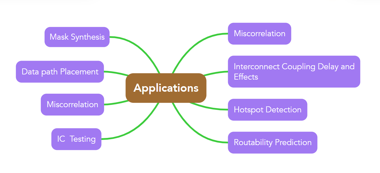
Figure 1. Applications of machine learning in IC design
2.1. Machine learning applied in mask/wafer hotspot detection
An essential first step in increasing manufacturability and reducing costs is the early discovery of lithography hotspots [5]. Although it takes a while, lithography simulation is accurate for hotspot identification. Therefore, it is essential to provide effective hotspot detection methods that have high accuracy in order to shorten the entire turnaround time. Lithography hotspot identification using machine learning is one of the phases in validation, which is also known as physical verification. In general, the purpose of hotspot detection is to model and classify the hotspots on the test layout based on the given data when two sets of hotspot and non-hotspot layout segments are provided. Figure 2 shows two examples of hotspot layouts.

Figure 2. Two hotspot layouts
Metrics for evaluating hotspot detection include false alarms and detection accuracy. The ratio of accurately detected hotspots to actual hotspots determines the detection accuracy, whereas the number of non-hotspots that are mistakenly classified as hotspots determines the false alarm rate. Layout feature extraction and model selection are two aspects that directly affect hotspot detection performance. The feature extraction technique based on fragmentation is shown in Figure 3(a). The effective radius r of each fragment F encompasses the neighbouring pieces. F includes the geometric details of the pieces covered by the circle, such as pattern forms, spacing between layouts, and corner information. The extraction approach for features using density is shown in Figure 3(c). The ratio of the layout to grid area is used to determine the layout's representation as a vector of pattern densities. It suggested to use concentric circles with area sampling to gather layout data that fits light diffraction, as seen in Figure 3(b). According to the researchers, this representations are lacking in spatial information. Since each feature taken from the layouts is kept in a feature vector, it is recommended to use feature tensor representation to preserve the spatial details of the layout. Figure 3 (d) displays the transformation of the original clips to hyper-image after feature tensor extraction. The original clip is split into 12 X 12 blocks, and each block is converted into a 100 X 100 image. After applying a discrete cosine transformation (DCT) to each block, the feature tensor is obtained.
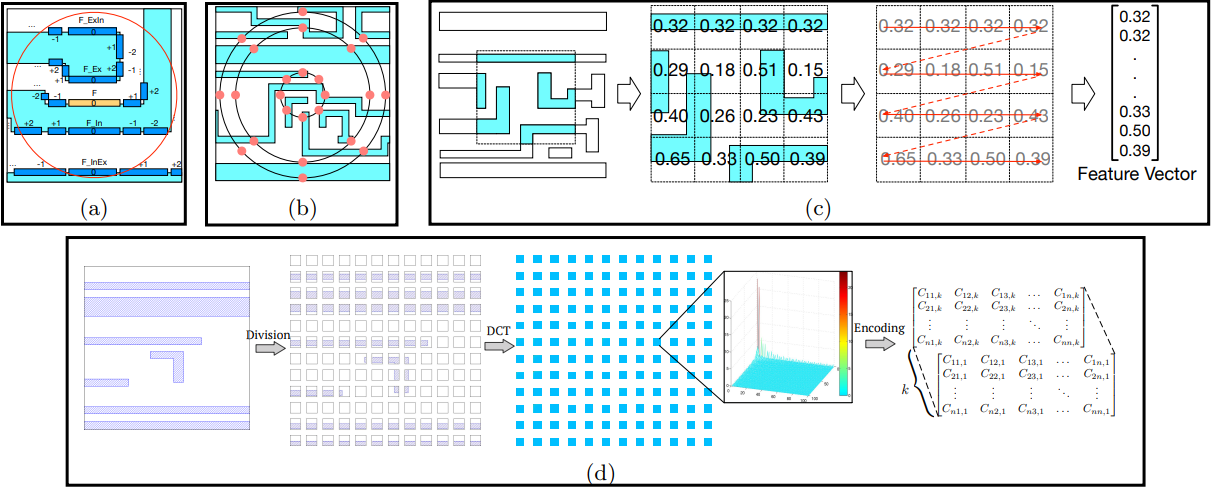
Figure 3(a). Fragmentation based hotspot signature extraction [6] (b). CCAS feature extraction [7] (c). Densitybased pattern representation [8] (d). Feature tensor generation [9]
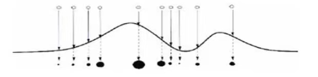
Because hotspot patterns frequently exhibit certain characteristics, by keeping a collection of hotspot patterns that have been previously described in a library, pattern matching is employed to address the detection issue. By comparing the topology of the input patterns to the topology of the patterns in the hotspot library, the problematic locations will be exposed to the operation of the pattern matching algorithms. The effectiveness of pattern matching-based hotspot identification is significantly influenced by the generality of the hotspot library. As a result, these methods perform poorly in advanced technology nodes with unknown topologies. [10] To enhance the hotspot identification result 25, a fuzzy matching model is presented to dynamically adjust the areas surrounding the recognized hotspot. Each known hotspot may be found using the pattern matching method, as shown in Figure 4, while the fuzzy region can repeatedly expand to increase precision.
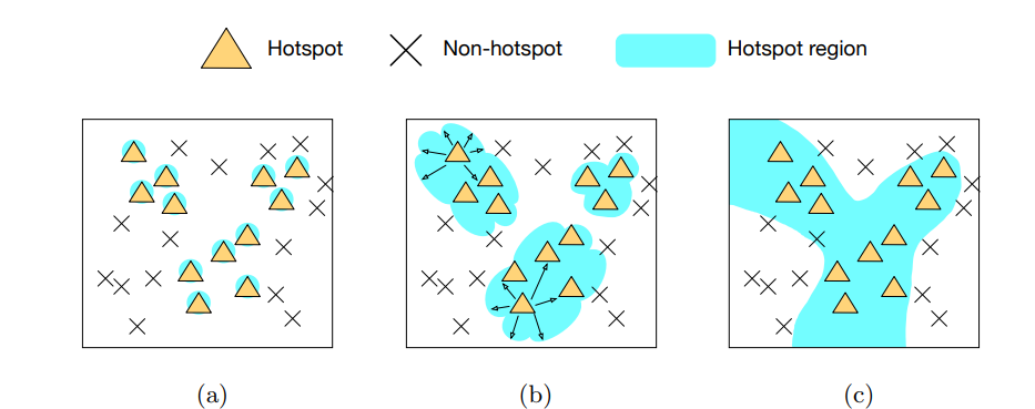
Figure 4: A 2D-space example . [(a) Pattern matching. (b) Fuzzy Pattern Matching. (c) Machine learning.
2.2. IC aging monitoring
The robustness and reliability issues that plague modern integrated circuits are exacerbated by aggressive scaling and process variations. The electrical behavior of transistors degrades over time due to various factors, and eventually leads to device failure as a result of extensive usage. Thus, runtime prediction of circuit performance degradation are critical to avoid severe consequences as a result of an unexpected run-time failure caused by ageing of the integrated circuits [11]. The analysis of IC run-time operating circumstances, the use of lookup tables to identify and anticipate performance deterioration, and other methods are traditional ways to assess the impact of ageing degradation in the area of operation. Due to its capacity to accurately and generally anticipate device aging-induced failure, a machine learning-based aging-prediction approach has recently attracted a lot of interest [12] [13]. The technique involves using a set of samples that includes values for both ageing indicator values (such as workload and temperature) and operating state parameter values (for example, critical path delays). Given new operating conditions, the trained model can then be used to predict the ageing indicator values.
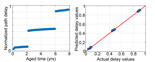
(a)
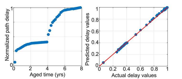
(b)
(c)
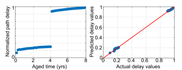
Figure 5. Aging degradation patterns and prediction results
The prediction results of the algorithm are shown in Figure 5. With the different amount of turning points of temperature (twice for Figure 5 (a); three times for Figure 5 (b); four times for Figure 5 (c)), the delay pattern appears to possess different times of sharp aging degradation accordingly. The machine learning algorithm was set up by filling parameters in formulated functions and performing regression. Finally, the prediction pattern is obtained. It can be seen that aging and degradation can be predicted with little error using ML models. Additionally, other techniques can also assist in predicting the aging condition, like the SVM regression model [14] and RNN model[15]. These models are all power full tools in the monitoring and maintaining of IC systems.
2.3. Machine learning applied in Power Analysis
Traditional methods for calculating power in VLSI circuits are increasingly difficult in more advanced circuits. The most dependable, but time-consuming, performance was obtained by simulation-based power computation. In this case, VLSI power computed using Monte-Carlo and other statistical methods is less dependent on simulation and yields more accurate results in less time. The Monte-Carlo techniques, also known as Monte-Carlo experiments, are computing algorithms that rely on repeated random sampling to provide numerical results (Figure 6). Power analysis at RTL or an enhanced abstraction level was studied. [16] To get correct power characterisation, a large amount of low-level information about the circuit must be represented, including standard cell characteristics, gate size and gating of the clock, and register location. They are used to calculate the switching capacitance and activity element of each circuit node in gate-level power estimates.
(a)
(b)
Figure 6 (a). Sample based Monte-Carlo (b). Sample algorithm
2.4. Possibility of Machine learning in IC design flow.
More broadly, during the whole IC design flow, applying machine learning to improve efficiency is an unstoppable trend. Traditional rule-based technology has reached its limits when it comes to handling EDA challenges with high dimensionality, discontinuities, and non-linearities as the IC industry becomes more and more complicated. Machine learning is in great demand to be involved in the flow of the IC industry. Aside from labour, the cost of SoC design includes time, hardware resources, and software resources. During the SoC design flow, some types of costs can be considered, such as correlation iteration, optimization time, sign-off time, and report review.
Table 1 lists industrial cases for the four previously mentioned compelling costs in the current circuit design flow, as well as feasible ML solutions. [17]
Table 1. Machine learning tool and concept
Cost | Industrial Case | ML solution (commercial tool, method...etc.) |
Correlation Literation | Global route vs. Detail route - Not fit well to certain design style - EDA vendors offer general | - in-house congestion predictor - routing engine embedded with machine learning |
Optimization Time | Power ECO (per run time x iteration) | Synopsis PrimeTime - ML optimization (embedded with circuit learning ability) |
Sign-off Time | IR Analysis (set selection) | ANSYS SeaHawk - ML screening (reduce set size) |
Report Review | Design rule violation / warning - Electrical - Physical | - ML clustering (each cluster is still judged by engineer) |
The trained model output was used as one of the constraints in the following iteration, and the data training process was previously independent of EDA tools, absorbing output from EDA tools. End-users may now access input/output data for EDA ML applications thanks to the development of integrated ML platforms by an increasing number of EDA solutions in recent years. When it comes to the near future of ML in EDA, machine learning as a service will be the trend. A large number of commercial data sets are offered via cloud services and APIs. Designers will eventually be able to use pre-built algorithms and models via cloud computing, and EDA providers will be able to offer ML features outside of enterprises. It is now possible to create a fully ML-driven IC design cycle, as shown in Figure 3, by adhering to a data sharing protocol that releases data for ML, thanks to the development of the foundry design ecosystem.
3. Conclusion
This paper has looked through the existing applications of artificial intelligence in the filed of integrated circuits design process, like mask/wafer hotspot detection, IC aging monitoring, and power analysis. Generally, machine learning can be applied in a lot of circumstances, which cover the whole lifetime of integrated circuits (manufacturing, testing, maintaining, etc.). It greatly saved the cost of labor and long-period development. The limitation of this paper is that the literature review can only reach the basic level of IC design, which mainly includes theories and algorithms. Actual cases or products can better illustrate the principle, and this paper lacks the relative resources to achieve this research level.
References
[1]. Hosmer Jr, D. W., Lemeshow, S., and Sturdivant, R. X., [Applied logistic regression], vol. 398, John Wiley & Sons (2013).
[2]. Freund, Y., Schapire, R. E., et al., “Experiments with a new boosting algorithm,” in [Icml], 96, 148–156 (1996). AdaBoost
[3]. Cortes, C. and Vapnik, V., “Support-vector networks,” Machine learning 20(3), 273–297 (1995). SVM.
[4]. Hornik, K., Stinchcombe, M., and White, H., “Multilayer feedforward networks are universal approximators,” Neural networks 2(5), 359–366 (1989).
[5]. Lin, Y. et al., 2017. Machine learning for mask/wafer hotspot detection and mask synthesis, 10451, pp.104510A–104510A-13.] [ E Poovannan, & S Karthik. (2021). Role Of Machine Learning In Vlsi Ic Design. Turkish Journal of Computer and Mathematics Education, 12(10), 2489–2494.
[6]. Ding, D., Torres, J. A., and Pan, D. Z., “High performance lithography hotspot detection with successively refined pattern identifications and machine learning,” IEEE Transactions on Computer-Aided Design of Integrated Circuits and Systems (TCAD) 30(11), 1621–1634 (2011).
[7]. Lin, S.-Y., Chen, J.-Y., Li, J.-C., Wen, W.-y., and Chang, S.-C., “A novel fuzzy matching model for lithography hotspot detection,” in [ACM/IEEE Design Automation Conference (DAC) ], (2013).
[8]. Zhang, H., Zhu, F., Li, H., Young, F. E., and Yu, B., “Bilinear lithography hotspot detection,” in [ACM International Symposium on Physical Design (ISPD) ], (2017).
[9]. Yang, H., Su, J., Zou, Y., Yu, B., and Young, F. E., “Layout hotspot detection with feature tensor generation and deep biased learning,” in [ACM/IEEE Design Automation Conference (DAC) ], (2017).
[10]. Yu, Y.-T., Chan, Y.-C., Sinha, S., Jiang, I. H.-R., and Chiang, C., “Accurate process-hotspot detection using critical design rule extraction,” in [ACM/IEEE Design Automation Conference (DAC) ], (2012).
[11]. Z. Yang, P. Sun, Y. Yu, H. Zhang, G. Gao, and X. Peng, “Workloadaware failure prediction method for VLSI devices using an LUT based approach,” in Proc. IEEE Int. Instrum. Meas. Technol. Conf., May 2018, pp. 1–6.], ageing sensors[M. Agarwal, B. C. Paul, M. Zhang, and S. Mitra, “Circuit failure prediction and its application to transistor aging,” in Proc. IEEE VLSI Test Symp., May 2007, pp. 277–286.
[12]. K. Huang, X. Zhang and N. Karimi, "Real-Time Prediction for IC Aging Based on Machine Learning," in IEEE Transactions on Instrumentation and Measurement, vol. 68, no. 12, pp. 4756-4764, Dec. 2019, doi: 10.1109/TIM.2019.2899477.
[13]. N. Karimi and K. Huang, "Prognosis of NBTI aging using a machine learning scheme," 2016 IEEE International Symposium on Defect and Fault Tolerance in VLSI and Nanotechnology Systems (DFT), 2016, pp. 7-10, doi: 10.1109/DFT.2016.7684060
[14]. A. Vijayan, A. Koneru, S. Kiamehr, K. Chakrabarty, and M. B. Tahoori, “Fine-grained aging-induced delay prediction based on the monitoring of run-time stress,” IEEE Trans. Comput.-Aided Design Integr. Circuits Syst., vol. 37, no. 5, pp. 1064–1075, May 2018.
[15]. R. J. Williams and D. Zipser, “A learning algorithm for continually running fully recurrent neural networks,” Neural Comput., vol. 1, no. 2, pp. 270–280, 1989.
[16]. A. B. Kahng, "New directions for learning-based IC design tools and methodologies," 2018 23rd Asia and South Pacific Design Automation Conference (ASP-DAC), 2018, pp. 405-410, doi: 10.1109/ASPDAC.2018.8297357.
[17]. L. Wang and M. Luo, "Machine Learning Applications and Opportunities in IC Design Flow," 2019 International Symposium on VLSI Design, Automation and Test (VLSI-DAT), 2019, pp. 1-3, doi: 10.1109/VLSI-DAT.2019.8742073.
Cite this article
Qiu,T. (2023). Application and possibility of machine learning in integrated circuit design. Applied and Computational Engineering,6,882-888.
Data availability
The datasets used and/or analyzed during the current study will be available from the authors upon reasonable request.
Disclaimer/Publisher's Note
The statements, opinions and data contained in all publications are solely those of the individual author(s) and contributor(s) and not of EWA Publishing and/or the editor(s). EWA Publishing and/or the editor(s) disclaim responsibility for any injury to people or property resulting from any ideas, methods, instructions or products referred to in the content.
About volume
Volume title: Proceedings of the 3rd International Conference on Signal Processing and Machine Learning
© 2024 by the author(s). Licensee EWA Publishing, Oxford, UK. This article is an open access article distributed under the terms and
conditions of the Creative Commons Attribution (CC BY) license. Authors who
publish this series agree to the following terms:
1. Authors retain copyright and grant the series right of first publication with the work simultaneously licensed under a Creative Commons
Attribution License that allows others to share the work with an acknowledgment of the work's authorship and initial publication in this
series.
2. Authors are able to enter into separate, additional contractual arrangements for the non-exclusive distribution of the series's published
version of the work (e.g., post it to an institutional repository or publish it in a book), with an acknowledgment of its initial
publication in this series.
3. Authors are permitted and encouraged to post their work online (e.g., in institutional repositories or on their website) prior to and
during the submission process, as it can lead to productive exchanges, as well as earlier and greater citation of published work (See
Open access policy for details).
References
[1]. Hosmer Jr, D. W., Lemeshow, S., and Sturdivant, R. X., [Applied logistic regression], vol. 398, John Wiley & Sons (2013).
[2]. Freund, Y., Schapire, R. E., et al., “Experiments with a new boosting algorithm,” in [Icml], 96, 148–156 (1996). AdaBoost
[3]. Cortes, C. and Vapnik, V., “Support-vector networks,” Machine learning 20(3), 273–297 (1995). SVM.
[4]. Hornik, K., Stinchcombe, M., and White, H., “Multilayer feedforward networks are universal approximators,” Neural networks 2(5), 359–366 (1989).
[5]. Lin, Y. et al., 2017. Machine learning for mask/wafer hotspot detection and mask synthesis, 10451, pp.104510A–104510A-13.] [ E Poovannan, & S Karthik. (2021). Role Of Machine Learning In Vlsi Ic Design. Turkish Journal of Computer and Mathematics Education, 12(10), 2489–2494.
[6]. Ding, D., Torres, J. A., and Pan, D. Z., “High performance lithography hotspot detection with successively refined pattern identifications and machine learning,” IEEE Transactions on Computer-Aided Design of Integrated Circuits and Systems (TCAD) 30(11), 1621–1634 (2011).
[7]. Lin, S.-Y., Chen, J.-Y., Li, J.-C., Wen, W.-y., and Chang, S.-C., “A novel fuzzy matching model for lithography hotspot detection,” in [ACM/IEEE Design Automation Conference (DAC) ], (2013).
[8]. Zhang, H., Zhu, F., Li, H., Young, F. E., and Yu, B., “Bilinear lithography hotspot detection,” in [ACM International Symposium on Physical Design (ISPD) ], (2017).
[9]. Yang, H., Su, J., Zou, Y., Yu, B., and Young, F. E., “Layout hotspot detection with feature tensor generation and deep biased learning,” in [ACM/IEEE Design Automation Conference (DAC) ], (2017).
[10]. Yu, Y.-T., Chan, Y.-C., Sinha, S., Jiang, I. H.-R., and Chiang, C., “Accurate process-hotspot detection using critical design rule extraction,” in [ACM/IEEE Design Automation Conference (DAC) ], (2012).
[11]. Z. Yang, P. Sun, Y. Yu, H. Zhang, G. Gao, and X. Peng, “Workloadaware failure prediction method for VLSI devices using an LUT based approach,” in Proc. IEEE Int. Instrum. Meas. Technol. Conf., May 2018, pp. 1–6.], ageing sensors[M. Agarwal, B. C. Paul, M. Zhang, and S. Mitra, “Circuit failure prediction and its application to transistor aging,” in Proc. IEEE VLSI Test Symp., May 2007, pp. 277–286.
[12]. K. Huang, X. Zhang and N. Karimi, "Real-Time Prediction for IC Aging Based on Machine Learning," in IEEE Transactions on Instrumentation and Measurement, vol. 68, no. 12, pp. 4756-4764, Dec. 2019, doi: 10.1109/TIM.2019.2899477.
[13]. N. Karimi and K. Huang, "Prognosis of NBTI aging using a machine learning scheme," 2016 IEEE International Symposium on Defect and Fault Tolerance in VLSI and Nanotechnology Systems (DFT), 2016, pp. 7-10, doi: 10.1109/DFT.2016.7684060
[14]. A. Vijayan, A. Koneru, S. Kiamehr, K. Chakrabarty, and M. B. Tahoori, “Fine-grained aging-induced delay prediction based on the monitoring of run-time stress,” IEEE Trans. Comput.-Aided Design Integr. Circuits Syst., vol. 37, no. 5, pp. 1064–1075, May 2018.
[15]. R. J. Williams and D. Zipser, “A learning algorithm for continually running fully recurrent neural networks,” Neural Comput., vol. 1, no. 2, pp. 270–280, 1989.
[16]. A. B. Kahng, "New directions for learning-based IC design tools and methodologies," 2018 23rd Asia and South Pacific Design Automation Conference (ASP-DAC), 2018, pp. 405-410, doi: 10.1109/ASPDAC.2018.8297357.
[17]. L. Wang and M. Luo, "Machine Learning Applications and Opportunities in IC Design Flow," 2019 International Symposium on VLSI Design, Automation and Test (VLSI-DAT), 2019, pp. 1-3, doi: 10.1109/VLSI-DAT.2019.8742073.