


1. Introduction
Perovskite solar cells (PSCs), illustrated in a formula of ABX3[1], are strikingly developed as a novel renewable technology choice to supplement former photovoltaic solar cell technologies. One vital factor deciding the photovoltaic efficiency and lifetime of the PSCs is the crystalline quality of perovskite films. Difficulties in precisely controlling the crystallization process of perovskite often result in undesirable morphology of the grain boundaries, film coverage, and trap states. Among the various techniques to improve device efficiency and stability, interfacial engineering (IE) with graphene quantum dots (GQDs) shows unique optical properties and good charge mobility for PSC application [2]. Experimentally, GQDs are shown to be convincing electrode modifiers to enhance the performance of PSC due to their increase in surface area and to fix the device’s aging due to their abundance of functional groups that can easily be non-toxically functionalize with organic and inorganic molecules [3].
As an additional process in the PSC fabrication, GQDs similarly possess various defects during their preparation. Du et al. introduce density functional theory (DFT) to traditional MAPbI3 perovskite film and obtain the result that interstitial defects often lead to creating electronic trap states [4]. Cuevas et al. substantiate the hypothesis that electronic trap states often correlate to structural defects like dislocations, grain boundaries, and impurities in inorganic semiconductors like multi-band PSCs [5]. When undergoing photoluminescence (PL) measurement, samples from solution-processed perovskite films are shown to have a decrease in PL lifetime compared to bulk single-crystal. This suggests the solution process with more sophisticated interfacial engineering needs to be well controlled to reduce substantial trap state concentration [6]. Moreover, Wetzelaer et al. use voltage-dependent electroluminescence to quantify the non-radiative recombination caused by trap states and conclude that electron traps are significant for the non-reversible drop in PSC performance [7].
Based on experimental results from the literature, we discuss the combined effect on the interfacial decoration of GQD/PSCs from the perspective of structural defects and trap states. In addition, this article provides a brief overview of recent developments in interfacial engineering mechanisms to control the structural defects of PSC.
2. Analysis
2.1. Structural Defects
In a perovskite solar cell, typically, the migration of an atom from its original crystal ABX3 structure originates structural defects [8], which alters the localized electronic energy states from their carrier conduction and valence bands (CB and VB). In this case, additional energy states are generated due to the trapped carriers, usually causing restrictions in their crystal mobility [9]. Interestingly, from the aspect of photovoltaics, the efficiency of solar cells can be improved by extending the cell response within the typically forbidden gap of the host semiconductor. If the sub-energy level is generated within the gap between the CB and VB, structural defects surprisingly do not restrict the photovoltaic emission intensities but allow the cell to respond more effectively to energy photons under the original bandgap.
Specifically, GQD/PSC can be generalized into surface defects [10], Stone-Wales (SW) defects, and edge defects. Surface defects in GQD/PSC usually occur between the boundaries of two thin films. Since there is no atom above the outer surface, the quantum dots on the shell are free to adjust their favorable locations, introducing defect states by C-OH and COOH functional groups on the perovskite film [11]. SW defects take place topologically in GQDs structure due to the rotation of C-C bonds [12]. Additional defects in perovskite crystal structures due to ion migration when a bias voltage is applied are systematically investigated by density functional calculations [13]. Such ion displacement may induce hysteresis in J-V curves, significant lattice distortion, and contraction leading to aging of PSC performance.
2.2. Trap states
Although defects in GQD/PSC can benefit the performance by providing more sub-energy states, the defective state will inevitably occur between the band edges (the gap between CB and VB) and permanently trap charges. In energy level structure, the shallow traps residing near band edges are revealed in a redshift PL measurement. On the other hand, deep traps between the CB and VB band typically hamper the anti-trapping process and cause the majority of non-radiative recombination, as depicted in Figure 1a [14].
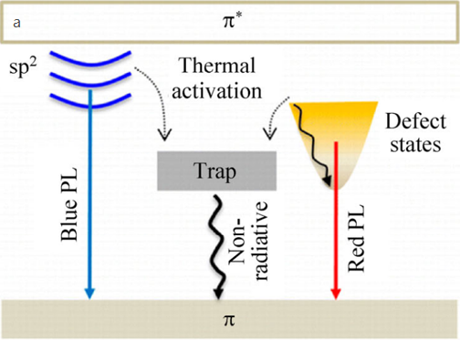
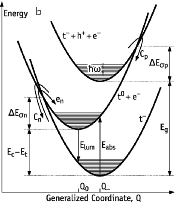
Figure (1a) Energy level structures incl, including photoexcited electrons' photovoltaic behaviors in GQDs. Reprinted with permission from Q. Xu et al., ACS Nano 7, 10654 (2013). (1b) Configuration coordinate diagram for an electron trap located at Ec-Et. Reprinted from Peaker et al., J. Appl. Phys. 123, 161559 (2018).
As shown in Figure 1b., w, photons are not involved in the measured photovoltaic transitioning and participate in non-radiatively Auger or multi-photon emission (MPE) mechanisms. The capture of a free hole, h+, for instance, is significantly detrimental to solar cells by creating a negatively charged trap with atomic configuration Q in the energy level diagram [15]. Both carrier types play a role in determining the device’s performance for PSCs. The theoretical mechanism of non-radiative recombination at a deep trap state is usually governed by Shockley-Read-Hall (SRH) statistics that depend on the single electron carrier capture rates [16]. Statistically, the rate at which a defect-generated trap captures an electron in a conduction band state (similarly to a valence band) is given by
\( {C_{n}}={σ_{n}}〈{v_{n}}〉n \) (1)
The thermally stimulated current (TSC) measurements in Figure 2. reveal the quantity and temperature-dependent distribution of electronic trap states in PSCs based on different thermal activation energies. Since the peaks in TSC are caused by the thermally distributed electronic trap states, the two low-temperature peaks (T1 and T2) indicate trap states’ existence in the PSC sample.
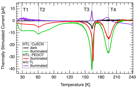
Figure 2. TSC plots reveal the qualified trap states in perovskite solar cells. Reprinted with permission from A. Baumann et al., J. Phys. Chem. Lett. 6, 12, 2350-2354 (2015).
Highly replied to the crystalline quality of the perovskite film, the trap density found in multi-crystalline silicon distributed between 1018 and 1021 m−3 like single-crystal structure [17]. Based on the integration of TSC results [18], under high sunlight intensities, the electronic trap state in GQD/PSC does not effectively hinder the device’s performance because the concentration of photovoltaic charge carriers is ten times more than that of the trap state concentration. However, the quantities of charge carriers and trap states are competitive at low light intensities. The defect-generated trap states in the perovskite layer certainly impact the PSC’s performance, as shown in Eq 2.
\( {I_{TSC}}=exp(−\frac{{E_{a}}}{{k_{B}}T}) \) (2)
2.3. Combine effect in GQD/PSC
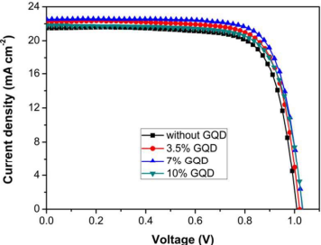
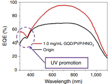
Figure 3. (a) Current density−voltage (J-V) curves of PSC/GQDs. Reprint with permission from X. Fang et al., Phys. Chem. Chem. Phys. 19, 6057-6063 (2017).
(b) External quantum efficiency curves of PSCs with GQD/PVP/HNO3. Reprinted with permission from X. Zhao et al., Nano Res., 1 (2021).
In Figure 3a. the improved perovskite solar cell efficiency (PCE) is caused by the increases in Voc, Jsc, and the Fill Factor (FF). The resulting measurements prove the hypothesis that GQDs modification can passivate the trap states existing at the perovskite grain boundaries. Consequently, non-radiative recombination is reduced, and electron extraction is improved for PCE. In the J-V curve, a 10% GQD coating trial does not have a greater interval than a 7% GQD coating trial. The drawback effect of too many quantum dots substantiates the suggestion that the regulation of fabricating GQD is crucial to idealizing PSC performance. The external quantum efficiency (EQE) is calculated to verify the increasing photocurrent, shown in Figure 3b. Compared to a pure PSC without the coating, GQD modification improves PSC performance from the visible wavelength region to the extent of the UV region.
3. Conclusion
The decoration of graphene quantum dots will create structural defects that benefit the performance of PSC by letting the photon respond below the energy band. The corresponding trap states, however, induce more non-radiative recombination that affects the aging of PSC. The overall performance of GQD/PSC shows that it is a promising method to improve the perovskite interface if the defects of adding graphene quantum dots are well controlled. During the synthesis of GQD and preparation of perovskite solar cell, annealing is typically a finalizing step, which, according to Ramen spectra, will cause a more disordered graphene structure [19, 20]. This paper proposes future research on GQDs modification to more variable device size, electrode film thickness, and perovskite lattice spacing control under well-controlling structure defects and traps states to optimize the favorable optical properties of decorated GQDs. Based on the simulation in the experimental condition, researchers can eventually develop industry-scale fabrication methods for GQD/PSC production with consistent surface structure and performance for every PSC to provide solar energy for a long lifetime.
References
[1]. Mritunjaya P., Ranbir S., Vivek K. S., Fabrication of Perovskite Solar Cells in Ambient Conditions, Mater. Today: Proc. 34, 3 (2021) 654-657.
[2]. Ponomarenko L. A., Schedin, F., Katsnelson, M. I., et al., A. K. Chaotic Dirac Billiard in Graphene Quantum Dots. Science. 320 (2008) 356-358.
[3]. Mehta, J., Bhardwaj, N., Bhardwaj, S., Tuteja, S., et al., A Graphene Quantum Dot Modified Screen Printed Immunosensor for the Determination of Parathion. Anal. Biochem. 523 (2017) 1-9.
[4]. Du, M. H. Efficient Carrier Transport in Halide Perovskites: Theoretical Perspectives. J. Mater. Chem. A. 2 (2014) 9091−9098.
[5]. Cuevas, A.; Stocks, M.; Macdonald, D.; Kerr, M.; Samundsett, C. Recombination and Trapping in Multicrystalline Silicon. Trans. Electron Devices 46 (1999) 2026−2034.
[6]. Shi, D.; Adinolfi, V.; Comin, R.; Yuan, M.; Alarousu, E.; Buin, A.; Chen, Y.; Hoogland, S.; Rothenberger, A.; Katsiev, K.; et al. Low TrapState Density and Long Carrier Diffusion in Organolead Trihalide Perovskite Single Crystals. Sci. 347 (2015) 519−522.
[7]. Wetzelaer, G.-J. A. H.; Scheepers, M.; Sempere, A. M.; Momblona, C.; Á vila, J.; Bolink, H. J. Trap-Assisted Non-Radiative Recombination in Organic−Inorganic Perovskite Solar Cells. Adv. Mater. 27 (2015) 1837−1841.
[8]. X. Yu, H. Cai, W. Zhang, X. Li, N. Pan, Y. Luo, X. Wang, J. G. Hou. Tuning Chemical Enhancement of SERS by Controlling the Chemical Reduction of Graphene Oxide Nanosheets. ACS Nano. 5 (2011) 952.
[9]. L. Ruiyi, P. Tinling, C. Hong-Xia, S. Jinsong, L. Zaijun. Electrochemical Detection of Cancer Cells in Human Blood Using Folic Acid and Glutamic Acid-functionalized Graphene Quantum Dot-palladium@Gold as Redox Probe with Excellent Electrocatalytic Activity and Target Recognition. Sens. Actuators B Chem. 309 (2020) 127709.
[10]. L. Vicarelli, S. J. Heerema, C. Dekker, H. W. Zandbergen. Controlling Defects in Graphene for Optimizing the Electrical Properties of Graphene Nanodevices. ACS Nano. 9 (2015) 3438.
[11]. L. G. Cançado, A. Jorio, E. H. M. Ferreira, F. Stavale, C. A. Achete, R. B. Capaz, M. V. O. Moutinho, A. Lombardo, T. S. Kulmala, A. C. Ferrari. Quantifying Defects in Graphene via Raman Spectroscopy at Different Excitation Energies. Nano Lett. 11 (2011) 3190.
[12]. R. Panyathip, S. Sucharitakul, S. Phaduangdhitidhada, A. Ngamjarurojana, P. Kumnorkaew, S. Choopun. Surface Enhanced Raman Scattering in Graphene Quantum Dots Grown via Electrochemical Process. Molecules. 26 (2021) 5484.
[13]. J. Haruyama, K. Sodeyama, L. Han, Y. Tateyama. First-Principles Study of Ion Diffusion in Perovskite Solar Cell Sensitizers. J. Am. Chem. Soc. 137, 32 (2015) 10048-10051.
[14]. H. Jin, E. Debroye, M. Keshavarz. It's a trap! On the Nature of the Localized States and Charge Trapping in Lead Halide Perovskites. Mater. Horiz. 7 (2020) 397-410.
[15]. A. Peaker, V. Markevich, J. Coutinho. Tutorial: Junction Spectroscopy Techniques and Deep-level Defects in Semiconductors. J. Appl. Phys. 123. (2018) 161559.
[16]. A Simplified Description of Recombination and Generation Lifetime with Worked Tutorial Examples Appears in D. K. Schroder, Semiconductor Materials and Device Characterization, 3rd ed. Chap. 7.
[17]. A. Cuevas, M. Stocks, D. McDonald, M. Kerr, C. Samundsett. Recombination and Trapping in Multicrystalline Silicon. Trans. Electron Devices. 46 (1999) 2026−2034.
[18]. A, Baumann, S. Väth, P. Rieder, M. C. Heiber, K. Tvingstedt. Identification of Trap States in Perovskite Solar Cells. J. Phys. Chem. Lett. 6, 12 (2015) 2350-2354.
[19]. X. Fang, J. Ding, N. Yuan. Graphene Quantum Dot Incorporated Perovskite Films: Passivating Grain Boundaries and Facilitating Electron Extraction. Phys. Chem. Chem. Phys. 19 (2017) 6057-6063.
[20]. G. Rajender, P. K. Giri. Formation Mechanism of Graphene Quantum Dots and Their Edge State Conversion Probed by Photoluminescence and Raman Spectroscopy. J. Mater. Chem. C. 4 (2016) 10852.
Cite this article
Zeng,C. (2023). Relation between structural defects and trap states in graphene quantum dots perovskite solar cell. Applied and Computational Engineering,7,24-28.
Data availability
The datasets used and/or analyzed during the current study will be available from the authors upon reasonable request.
Disclaimer/Publisher's Note
The statements, opinions and data contained in all publications are solely those of the individual author(s) and contributor(s) and not of EWA Publishing and/or the editor(s). EWA Publishing and/or the editor(s) disclaim responsibility for any injury to people or property resulting from any ideas, methods, instructions or products referred to in the content.
About volume
Volume title: Proceedings of the 3rd International Conference on Materials Chemistry and Environmental Engineering (CONF-MCEE 2023), Part II
© 2024 by the author(s). Licensee EWA Publishing, Oxford, UK. This article is an open access article distributed under the terms and
conditions of the Creative Commons Attribution (CC BY) license. Authors who
publish this series agree to the following terms:
1. Authors retain copyright and grant the series right of first publication with the work simultaneously licensed under a Creative Commons
Attribution License that allows others to share the work with an acknowledgment of the work's authorship and initial publication in this
series.
2. Authors are able to enter into separate, additional contractual arrangements for the non-exclusive distribution of the series's published
version of the work (e.g., post it to an institutional repository or publish it in a book), with an acknowledgment of its initial
publication in this series.
3. Authors are permitted and encouraged to post their work online (e.g., in institutional repositories or on their website) prior to and
during the submission process, as it can lead to productive exchanges, as well as earlier and greater citation of published work (See
Open access policy for details).
References
[1]. Mritunjaya P., Ranbir S., Vivek K. S., Fabrication of Perovskite Solar Cells in Ambient Conditions, Mater. Today: Proc. 34, 3 (2021) 654-657.
[2]. Ponomarenko L. A., Schedin, F., Katsnelson, M. I., et al., A. K. Chaotic Dirac Billiard in Graphene Quantum Dots. Science. 320 (2008) 356-358.
[3]. Mehta, J., Bhardwaj, N., Bhardwaj, S., Tuteja, S., et al., A Graphene Quantum Dot Modified Screen Printed Immunosensor for the Determination of Parathion. Anal. Biochem. 523 (2017) 1-9.
[4]. Du, M. H. Efficient Carrier Transport in Halide Perovskites: Theoretical Perspectives. J. Mater. Chem. A. 2 (2014) 9091−9098.
[5]. Cuevas, A.; Stocks, M.; Macdonald, D.; Kerr, M.; Samundsett, C. Recombination and Trapping in Multicrystalline Silicon. Trans. Electron Devices 46 (1999) 2026−2034.
[6]. Shi, D.; Adinolfi, V.; Comin, R.; Yuan, M.; Alarousu, E.; Buin, A.; Chen, Y.; Hoogland, S.; Rothenberger, A.; Katsiev, K.; et al. Low TrapState Density and Long Carrier Diffusion in Organolead Trihalide Perovskite Single Crystals. Sci. 347 (2015) 519−522.
[7]. Wetzelaer, G.-J. A. H.; Scheepers, M.; Sempere, A. M.; Momblona, C.; Á vila, J.; Bolink, H. J. Trap-Assisted Non-Radiative Recombination in Organic−Inorganic Perovskite Solar Cells. Adv. Mater. 27 (2015) 1837−1841.
[8]. X. Yu, H. Cai, W. Zhang, X. Li, N. Pan, Y. Luo, X. Wang, J. G. Hou. Tuning Chemical Enhancement of SERS by Controlling the Chemical Reduction of Graphene Oxide Nanosheets. ACS Nano. 5 (2011) 952.
[9]. L. Ruiyi, P. Tinling, C. Hong-Xia, S. Jinsong, L. Zaijun. Electrochemical Detection of Cancer Cells in Human Blood Using Folic Acid and Glutamic Acid-functionalized Graphene Quantum Dot-palladium@Gold as Redox Probe with Excellent Electrocatalytic Activity and Target Recognition. Sens. Actuators B Chem. 309 (2020) 127709.
[10]. L. Vicarelli, S. J. Heerema, C. Dekker, H. W. Zandbergen. Controlling Defects in Graphene for Optimizing the Electrical Properties of Graphene Nanodevices. ACS Nano. 9 (2015) 3438.
[11]. L. G. Cançado, A. Jorio, E. H. M. Ferreira, F. Stavale, C. A. Achete, R. B. Capaz, M. V. O. Moutinho, A. Lombardo, T. S. Kulmala, A. C. Ferrari. Quantifying Defects in Graphene via Raman Spectroscopy at Different Excitation Energies. Nano Lett. 11 (2011) 3190.
[12]. R. Panyathip, S. Sucharitakul, S. Phaduangdhitidhada, A. Ngamjarurojana, P. Kumnorkaew, S. Choopun. Surface Enhanced Raman Scattering in Graphene Quantum Dots Grown via Electrochemical Process. Molecules. 26 (2021) 5484.
[13]. J. Haruyama, K. Sodeyama, L. Han, Y. Tateyama. First-Principles Study of Ion Diffusion in Perovskite Solar Cell Sensitizers. J. Am. Chem. Soc. 137, 32 (2015) 10048-10051.
[14]. H. Jin, E. Debroye, M. Keshavarz. It's a trap! On the Nature of the Localized States and Charge Trapping in Lead Halide Perovskites. Mater. Horiz. 7 (2020) 397-410.
[15]. A. Peaker, V. Markevich, J. Coutinho. Tutorial: Junction Spectroscopy Techniques and Deep-level Defects in Semiconductors. J. Appl. Phys. 123. (2018) 161559.
[16]. A Simplified Description of Recombination and Generation Lifetime with Worked Tutorial Examples Appears in D. K. Schroder, Semiconductor Materials and Device Characterization, 3rd ed. Chap. 7.
[17]. A. Cuevas, M. Stocks, D. McDonald, M. Kerr, C. Samundsett. Recombination and Trapping in Multicrystalline Silicon. Trans. Electron Devices. 46 (1999) 2026−2034.
[18]. A, Baumann, S. Väth, P. Rieder, M. C. Heiber, K. Tvingstedt. Identification of Trap States in Perovskite Solar Cells. J. Phys. Chem. Lett. 6, 12 (2015) 2350-2354.
[19]. X. Fang, J. Ding, N. Yuan. Graphene Quantum Dot Incorporated Perovskite Films: Passivating Grain Boundaries and Facilitating Electron Extraction. Phys. Chem. Chem. Phys. 19 (2017) 6057-6063.
[20]. G. Rajender, P. K. Giri. Formation Mechanism of Graphene Quantum Dots and Their Edge State Conversion Probed by Photoluminescence and Raman Spectroscopy. J. Mater. Chem. C. 4 (2016) 10852.