


1. Introduction
The semiconductor industry has gone through three stages. The first generation of semiconductor material is represented by silicon (Si), which has been industrialized and widely used. The material of the second-generation semiconductor is arsenalized Gallium (GaAs) which has also been widely used. The third-generation semiconductor is represented by Gallium Nitride (GaN) and Silicon Carbide (SiC), Zinc Oxide (ZnO) and other wide forbidden belts.
In the meantime, people have put forward new requirements for the performance of power devices with the popularity of new energy, 5G communications, electric vehicles and smart industry. However, traditional silicon devices which have reached their physical limit due to the material characteristics can not meet the emerging needs in terms of performance. As a result, people are pinning their hopes on the third-generation semiconductors (GaN and SiC), which have excellent electrical properties [1]. This paper will talk about the third-generation semiconductors from three aspects: characteristics, application and development trend. In addition, this paper will help those who want to get some information about the third-generation semiconductor roughly.
2. Characteristics
Compared with the previous two generations of products, the third-generation of semiconductor has a number of advantages. SiC and GaN are the most promising wide-band-gap semiconductors, and SiC was developed earlier. The gap width of SiC and GaN is much larger than that of Si and GaAs, and the corresponding intrinsic carrier concentration is less than that of Si and GaAs.
GaN | GaAs | Si | |
Band gap | 3.42 eV | 1.42 eV | 1.12 eV |
Electron mobility | 2000 cm2/Vs | 6000 cm2/Vs | 600 cm2/Vs |
Breakdown voltage | 3.3 MV/cm | 0.5 MV/cm | 0.4 MV/cm |
Thermal conductivity | 1.3 W/cm/k | 0.5 W/cm/k | 1.5 W/cm/k |
Table 1. characteristics parameters of different semiconductor materials [1]
Take gallium nitride as an example. According to the table 1, the band gap and electron mobility of GaN are almost four times that of the first generation semiconductor Si. At the same time, the breakdown voltage of GaN is much higher than that of Si, so it is more difficult for the semiconductor made of gallium nitride to be breakdown. Which also means that it is safer and longer service life when use it.
In the meantime, the third-generation semiconductor is also better than the first one in heat conductivity and radiation resistance. Figure 1 shows the characteristic comparison between different generations of semiconductor materials.
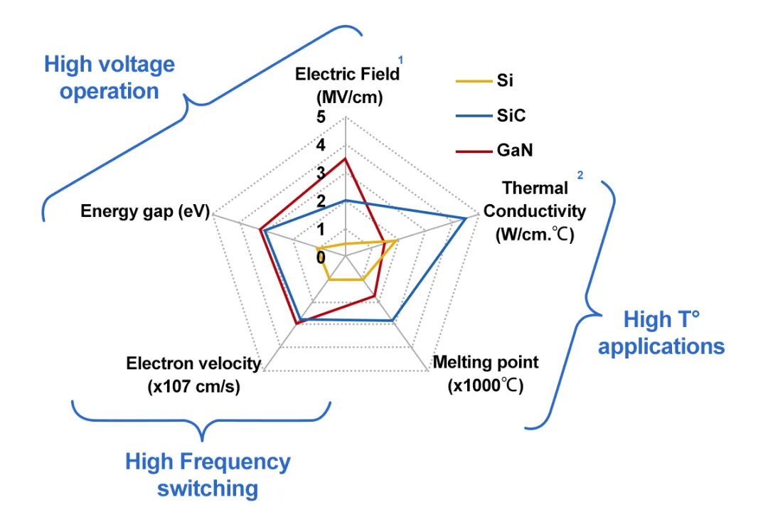
Figure 1. Characteristic comparison between different generations of semiconductor materials [2]
This figure shows that, the third-generation semiconductor is suitable for producing high-frequency switching and being used in high voltage operation and high thermal applications. For example, under the criteria of Figure 1, each data for SiC outperforms Si. SiC has a wide band gap, high breakdown electric field, high thermal conductivity and high electron saturation rate. For example, 4H-SiC MESFET has the advantages of high frequency and high power, normal operation under high temperature and radiation conditions, and small-size heat dissipation accessories [3]. Therefore, Jia Lin and Haosheng Huang pointed out that the third-generation of semiconductor is also known as the "Core" of solid-state light source, power electronics, microwave RF devices, and the "New engine" of the optoelectronics and microelectronics industry [4].
On the other hand, by changing the doping material of the third-generation semiconductor, people are also able to get many products with great performance. Basically, n-type semiconductors can be formed by doping N or P into SiC. At the same time, P-type semiconductors can be formed by doping Al, B, Ga and Be. Dr. Wu, Changchun Institute of Optics, Fine Mechanics and Physics, Chinese Academy of Sciences pointed out that doping silicon carbide heavily with boron, aluminum, or nitrogen can give the doped silicon carbide an order of magnitude electrical conductivity comparable to that of metals [5]. In addition, Li and Deng also showed that SiC has superconductivity At a temperature of 1.5K when Al or B is doped [2].
Although the performance of the third-generation semiconductor is better than the first-generation semiconductors. the manufacturing costs of the third-generation semiconductor is higher than the first. SiC products are about four times more expensive than silicon products when they have both the same characteristics and used in the same conditions.
3. Application
At present, the third-generation semiconductor can be mainly used in photoelectric, microwave RF, and power electronics fields.
3.1. Photoelectric field
The field of optoelectronics is the most mature application field so far. It not only has a scale of hundreds of billions of dollars, but also a successful technological revolution. The current application scope includes display, backlight, lighting and so on.
Take the Blue LED as an example. Blue LED chips are able to be made from the third-generation semiconductor. The energetic photons display blue light. Therefore, the semiconductor which is used to produce blue light should have a wide band width. Neither the first nor second-generation semiconductor belts reach this width. Therefore people use the third-generation semiconductor (wide-band semiconductors) to product the blue LED chips. In 1972, Herb Maruska and Wally Rhines et al, who from Stanford University reported Mg-doped GaN LED of green and blue colors for the first time [6].
3.2. Microwave and radio frequency
Microwave and radio frequencies mainly cover various high-tech fields, such as automotive radar, satellite communication, 5G communication systems, early warning detection and so on. Take the 5G communication systems as an example. Due to the continuous advancement of 5G communication systems, such materials that have the performance advantages of SiC wide band gap will become even more important.
The third-generation semiconductors are used in the construction of 5G communication systems because of it outstanding characteristics. The third-generation semiconductor can keep the original conductivity and keep the equipment running in the high temperature and high radiation environment under the condition of high temperature and great change of external energy. SiC and GaN are able to work in the environment of 600 ℃ or above with high power density radio frequency (RF) electrons, which is the research focus of semiconductor science, high temperature electronics, high power microwave electronics and so on.
For example, Giovanni Santoruvo and Elison Matioli have developed devices that can be used in high-frequency radio-frequency applications in 2017 [7].
All of the above features are beneficial to the establishment of 5G communication systems. 5G systems require ever-increasing bandwidth for mobile base stations. On the other hand the RF power amplifier consume a lot of energy. In these reasons, it is important to look for lighter, smaller, cheaper alternatives. As new materials, SiC and GaN have shown great advantages in devices. The application of these materials in 5G communication equipment is of great significance. GaN-based RF devices can provide higher operating voltage, increasing power density while meeting the operating frequency and bandwidth requirements. Because of the advantage of the nature of gallium nitride material, more and more researchers begin to use it in the 5G research. At present, gallium nitride is an ideal RF power device material for 5G wireless communication networks [8].
3.3. Power Electronics
Power electronics are now widely used in the economy and life, such as smart grids, new energy vehicles, rail transit, renewable energy development, industrial motors, data centers, household appliances, and mobile electronic equipment. Power electronics are indispensable core semiconductor products in the industrial system. Among them, SiC power devices, which are considered to be the largest application market in the future in new energy vehicles, are mainly used in power control units (PCUs), inverters, DC-DC converters, on-board chargers and so on. In addition, GaN power devices are also used in the power electronics field due to their high frequency. The high efficiency has great application potential in consumer electronics chargers, new energy charging piles, data centers, and other fields.
Take the new energy vehicles as an example. The following figure, which is from DeepTech, shows the application of SiC, GaN new energy vehicle.
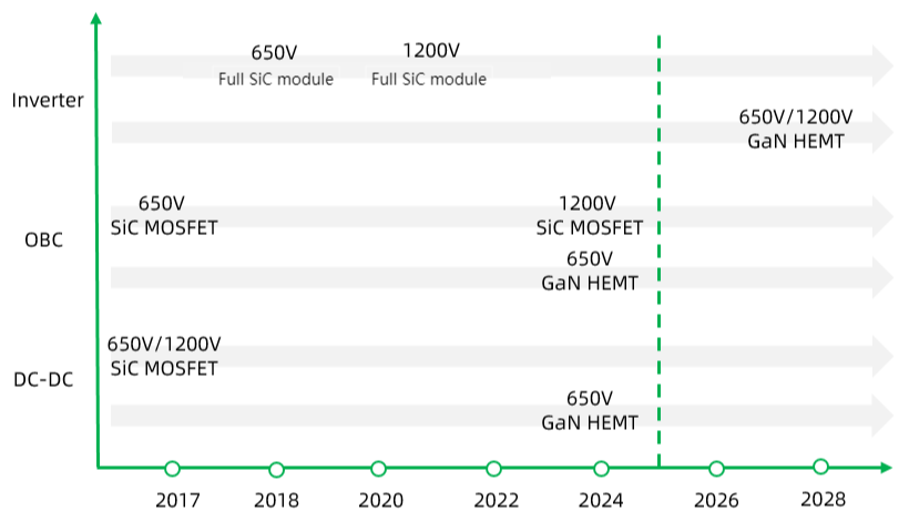
Figure 2. SiC, GaN new energy vehicle application Road map
SiC power electronic devices have been used in new energy vehicles and they have a tendency to replace Si IGBT in main drive inverters. After Tesla first adopted the inverter of SIC Power Module, BYD followed closely behind. At the same time, other Original Equipment Manufacturer also began to lay out. The market outlook for SIC is predictable. It is expected that the SiC will be used in mid-to low-end vehicles by 2025 [9]. By then, the market will have been launched on a large scale, and the SIC market may be in short supply.
GaN power electronics in the short term may not have a major opportunity. However, GaN has a bright future in the medium and long term. The first applications of GaN in new energy vehicles may be OBC or lidar [9]. In the long run, if GaN proves its reliability and high current capability at a lower price, it could penetrate the more challenging new energy vehicle inverter market to compete with SIC and Si.
At the same time, power electronics in new energy vehicles also use LEDs. The new energy vehicle display market will develop from LCD to Mini/Micro-LED gradually. A Micro-LED display is expected to become the ultimate solution. Mini-led car applications have been achieved. AUO has launched a Micro-LED car display. Micro-LED is expected to achieve car applications in 2025.
4. Development trend
4.1. Larger wafers will become mainstream, and material quality and device performance will continue to improve
Production cost is the main driving force of large-size wafer, and larger wafer diameter can increase single-crystal utilization and reduce wafer manufacturing costs. Therefore, the continuous development of new processes and new technologies to reduce the density of defects in materials, improve product yield and reduce costs, accelerating the breakthrough of substrate materials, epitaxy, chip and packaging testing bottlenecks, will become the main theme of the entire industry in the future.
4.2. Third-generation semiconductors will be used in more field
Third-generation semiconductor materials have obvious advantages in the application of new energy vehicles, PV, consumer electronics, rail transportation, light-emitting diode, 5G RF and so on. As of 2019, third-generation semiconductor devices patents are distributed in the 8 volumes of IPC, and mainly distributed in H "Electricity", C "Chemistry; Metallurgy", G "Physics" and B "Processing; Transportation". The total proportion of these four volumes reaches 99.07% of the total patents [10]. Therefore, the application of the third-generation semiconductor in various industries will gradually increase with the third-generation semiconductor mass production technology breakthrough and the reduction of cost.
4.3. The new material system will gradually mature
UWB bandgap list of semiconductor materials such as Gao, AlN, and diamond have the characteristics of higher breakdown voltage, lower resistance, higher frequency, and higher power than SiC and GaN. It is the key core material to support the innovative development, transformation and upgrading of the future rail transit, new energy vehicles, energy internet and other industries.
5. Conclusion
This paper introduces the characteristics, applications and development trends of the third-generation semiconductor. Compared with the first-generation and second-generation semiconductors, the third-generation semiconductor has a wider bandgap width, higher breakdown electric field, higher thermal conductivity and higher electron saturation rate. These characteristics make third-generation semiconductor more suitable for producing high-temperature, high-frequency, and high-power devices. After that, the paper introduces three main application directions of the third-generation semiconductor, which are photoelectric, microwave RF and power electronics. Finally, the paper wrote the third-generation semiconductor development trends and proposed three trends. In the future, larger wafers will become mainstream. The third-generation semiconductors will be used in more fields. In addition, the new material system will gradually mature.
In conclusion, the development of third-generation semiconductors is fast and efficient in general. Although there are still some problems to be solved at this stage, such as the high cost of manufacturing third-generation semiconductors. In the foreseeable future, these problems will be solved and the third-generation semiconductor will become an indispensable part of people's production and lives. The paper still has some limitations. One of the limitations is that data and experiments are not involved in this paper. In the future, the author will conduct relevant experiments and collect experimental data to overcome this limitation.
References
[1]. Xinrong Xie, “The Research Progress of The third-generation Semiconductor Materials GaN”, Guangdong Chemical Industry, vol. 47, pp. 92-93, Dec. 2020. DOI: 10.3969/j.issn.1007-1865.2020.18.039
[2]. Chun Li and Junkai Deng, “Analysis of the third-generation Semiconductor Industry”, Integrated circuit applications, vol. 34, no. 2, pp. 87-99, Feb. 2017. DOI: 10.19339/j.issn.1674-25832017.02.023
[3]. Baolin Zhang et al, “Application of third-generation Wide-gap Semiconductor (SiC) Devices in Space Solar Power Station ”, SPACE ELECTRONIC TECHNOLOGY, vol. 15, no. 2, pp. 94-100, Feb. 2018. DOI: 10. 3969 / j. issn. 1674-7135. 2018. 02. 015
[4]. Jia Lin and Haosheng Huang, “Opportunities and Challenges by the third-generation Semiconductor”, Integrated circuit applications, vol. 34, no. 12, pp. 83-86, Dec. 2017. DOI: 10.19339/j.issn.1674-2583.2017.12.021
[5]. Na Wu, “Theoretical model of holographic grating mask pattern transfer and research on new technology”, Doctoral dissertation of Changchun Institute of Optics, Fine Mechanics and Physics, Chinese Academy of Sciences, May. 2013.
[6]. S. Nakamura, M. Senoh, N. Iwasa and S. N. S. Nagahama, "High-Brightness InGaN Blue Green and Yellow Light-Emitting Diodes with Quantum Well Structures", Jpn. J. Appl. Phys, vol. 34, no. 7A, pp. L797, Jul. 1995.
[7]. G. Santoruvo and E. Matioli, "In-Plane-Gate GaN Transistors for High-Power RF Applications," in IEEE Electron Device Letters, vol. 38, no. 10, pp. 1413-1416, Oct. 2017, DOI: 10.1109/LED.2017.2737658.
[8]. Xianjie Zhang, “Development and Opportunity of the third-generation Semiconductor Materials in 5G Communication Field ”, HEILONGJIANG SCIENCE, vol. 11, no. 20, pp. 42 and 45, Oct. 2020
[9]. DeepTech, “Technology development path and industrial ecology research report on the application of third-generation semiconductor SiC/GaN in new energy vehicles in 2022”.
[10]. Nong Li et al, “Patent Analysis of the third-generation Semiconductor Devices”, Technology Intelligence Engineering, vol. 5, no. 4, pp. 114-126, Apr. 2019. DOI: 10.3772/j.issn.2095-915x.2019.04.012
Cite this article
Tang,M. (2023). Characteristics, application and development trend of the third-generation semiconductor. Applied and Computational Engineering,7,41-46.
Data availability
The datasets used and/or analyzed during the current study will be available from the authors upon reasonable request.
Disclaimer/Publisher's Note
The statements, opinions and data contained in all publications are solely those of the individual author(s) and contributor(s) and not of EWA Publishing and/or the editor(s). EWA Publishing and/or the editor(s) disclaim responsibility for any injury to people or property resulting from any ideas, methods, instructions or products referred to in the content.
About volume
Volume title: Proceedings of the 3rd International Conference on Materials Chemistry and Environmental Engineering (CONF-MCEE 2023), Part II
© 2024 by the author(s). Licensee EWA Publishing, Oxford, UK. This article is an open access article distributed under the terms and
conditions of the Creative Commons Attribution (CC BY) license. Authors who
publish this series agree to the following terms:
1. Authors retain copyright and grant the series right of first publication with the work simultaneously licensed under a Creative Commons
Attribution License that allows others to share the work with an acknowledgment of the work's authorship and initial publication in this
series.
2. Authors are able to enter into separate, additional contractual arrangements for the non-exclusive distribution of the series's published
version of the work (e.g., post it to an institutional repository or publish it in a book), with an acknowledgment of its initial
publication in this series.
3. Authors are permitted and encouraged to post their work online (e.g., in institutional repositories or on their website) prior to and
during the submission process, as it can lead to productive exchanges, as well as earlier and greater citation of published work (See
Open access policy for details).
References
[1]. Xinrong Xie, “The Research Progress of The third-generation Semiconductor Materials GaN”, Guangdong Chemical Industry, vol. 47, pp. 92-93, Dec. 2020. DOI: 10.3969/j.issn.1007-1865.2020.18.039
[2]. Chun Li and Junkai Deng, “Analysis of the third-generation Semiconductor Industry”, Integrated circuit applications, vol. 34, no. 2, pp. 87-99, Feb. 2017. DOI: 10.19339/j.issn.1674-25832017.02.023
[3]. Baolin Zhang et al, “Application of third-generation Wide-gap Semiconductor (SiC) Devices in Space Solar Power Station ”, SPACE ELECTRONIC TECHNOLOGY, vol. 15, no. 2, pp. 94-100, Feb. 2018. DOI: 10. 3969 / j. issn. 1674-7135. 2018. 02. 015
[4]. Jia Lin and Haosheng Huang, “Opportunities and Challenges by the third-generation Semiconductor”, Integrated circuit applications, vol. 34, no. 12, pp. 83-86, Dec. 2017. DOI: 10.19339/j.issn.1674-2583.2017.12.021
[5]. Na Wu, “Theoretical model of holographic grating mask pattern transfer and research on new technology”, Doctoral dissertation of Changchun Institute of Optics, Fine Mechanics and Physics, Chinese Academy of Sciences, May. 2013.
[6]. S. Nakamura, M. Senoh, N. Iwasa and S. N. S. Nagahama, "High-Brightness InGaN Blue Green and Yellow Light-Emitting Diodes with Quantum Well Structures", Jpn. J. Appl. Phys, vol. 34, no. 7A, pp. L797, Jul. 1995.
[7]. G. Santoruvo and E. Matioli, "In-Plane-Gate GaN Transistors for High-Power RF Applications," in IEEE Electron Device Letters, vol. 38, no. 10, pp. 1413-1416, Oct. 2017, DOI: 10.1109/LED.2017.2737658.
[8]. Xianjie Zhang, “Development and Opportunity of the third-generation Semiconductor Materials in 5G Communication Field ”, HEILONGJIANG SCIENCE, vol. 11, no. 20, pp. 42 and 45, Oct. 2020
[9]. DeepTech, “Technology development path and industrial ecology research report on the application of third-generation semiconductor SiC/GaN in new energy vehicles in 2022”.
[10]. Nong Li et al, “Patent Analysis of the third-generation Semiconductor Devices”, Technology Intelligence Engineering, vol. 5, no. 4, pp. 114-126, Apr. 2019. DOI: 10.3772/j.issn.2095-915x.2019.04.012