


1. Introduction
Over the past decade, the number of global internet users has experienced a blowout growth, and the explosive data traffic has exceeded the processing limits of traditional electronic devices. According to Cisco's 2020 Annual Internet White Paper, the number of global IoT users was only 3.9 billion in 2018, but it surged to 5.3 billion just five years later, accounting for 66% of the global population [1]. Meanwhile, with the comprehensive deployment of 5G networks, the average speed of global networks has also seen a comprehensive improvement, thereby bringing richer application scenarios - 4K/8K ultra-high-definition video, cloud gaming, telemedicine, industrial Internet, etc. Behind the data flood lies the urgent demand for high-speed, low-power, and small-sized devices in optical interconnect technology. However, the traditional electro-optic conversion architecture based on silicon-based modulators has always faced an irreconcilable contradiction between bandwidth, drive power consumption, and CMOS process compatibility. When the modulation rate exceeds 70 GHz, devices often need to make significant compromises in terms of modulation depth, insertion loss, or drive voltage, thus limiting their development in the field of ultra-high-speed optical interconnects in the future [2].
Under this background, graphene, with its unique zero bandgap structure, carrier mobility as high as 2×105cm2V-1S-1 at room temperature, and efficient response across the visible to far-infrared spectrum, is pushing the three parameters of bandwidth, speed, and CMOS compatibility to new limits [3]. Zero bandgap means that the valence band and conduction band of graphene are directly connected at the Dirac point, allowing electrons to be excited without crossing the forbidden band, which fundamentally eliminates the time delay of carrier transitions. The ultra-high carrier mobility enables these electron-hole pairs to complete acceleration, drift, and recombination within sub-picosecond time scales, providing devices with intrinsic broadband far exceeding that of traditional semiconductors (such as InP and GaAs). The wide-band response also enables efficient absorption and refractive index tuning in visible, near-infrared, and even high-infrared communication windows, thus eliminating material constraints on specific wavelength bands and reducing process complexity and cost. The combination of these three factors allows it to simultaneously break through a series of bottlenecks in bandwidth, speed, and CMOS compatibility in optical communication modulation, thus opening up a new path for building high-speed, low-drive-voltage, and low-power optical modulators [3].
Based on this, this paper sorts out the physical mechanism of graphene optical modulation, summarizes the latest progress of graphene-based optical communication modulators in device structure, performance indicators, and integration processes since 2020, and discusses a series of challenges that graphene still needs to overcome in this field. It aims to provide a panoramic reference for scientific researchers and engineering technicians, accelerating the breakthrough and implementation of the next-generation ultra-high-speed and low-power optical interconnection technology.
2. The optical modulation mechanism of graphene
2.1. Saturable absorption characteristics
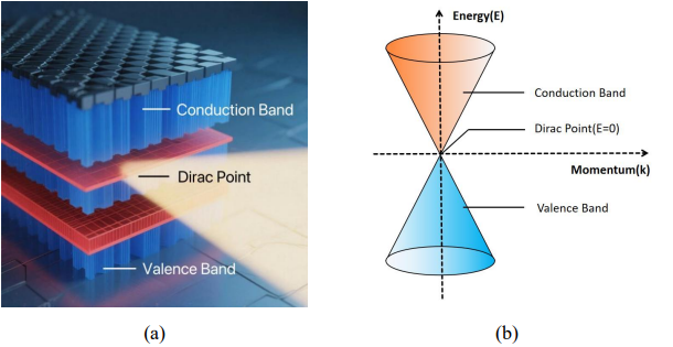
Graphene is a zero-bandgap material, with its valence band and conduction band directly connected at the Dirac point. As shown in Figure 1(a), the schematic diagram of the graphene band structure demonstrates the relative positions among the three. In addition, its linear dispersion relationship is usually shown by a Dirac cone as shown in Figure 1(b), where the horizontal axis represents momentum k and the vertical axis represents energy E. The upper half-cone (E>0) is the conduction band, the lower half-cone (E<0) is the valence band, and the intersection point E=0 is the Dirac point. Because there is no place to accommodate electrons at this point, electrons can transition instantaneously without overcoming the band gap, thus enabling graphene to exhibit ultra-fast response in the optical communication band. However, when the light intensity exceeds the saturation absorption threshold of graphene (0.5MWcm-2), the valence band at the top and the conduction band at the bottom are respectively filled with photogenerated electrons and holes, generating the Pauli blocking effect, which can no longer accommodate new electron pairs. As a result, the absorption coefficient decreases with the increase of light intensity, thereby achieving all-optical modulation that varies with light intensity [4].
2.2. Light causes changes in refractive index
The third-order nonlinear susceptibility of graphene is a core parameter that describes its ability to undergo strong light-induced refractive index changes. Its physical meaning can be described using the general expression for nonlinear optics:
Where
Under the same light intensity
2.3. Plasma coupling
Coupling graphene with metal nanostructures can compress the light field to a deep subwavelength size, raising the intensity of the interaction between light and matter by two orders of magnitude. The principle lies in that when the free electrons on the metal surface resonate with the incident light, forming surface plasmon polaritons (SPP), the local field strength can be enhanced by 80 times [7]. Its core value lies in breaking the contradiction between the "light field constraint range" and the "intensity of light and matter interaction" in traditional optical modulation, providing a brand-new path for the construction of miniaturized and high-performance modulator devices. Qu et al. took advantage of this property to couple silver nanowire -MIM gaps with single-layer graphene, increasing the light absorption cross-section by 1-2 levels. They adjusted the Fermi level E-F of graphene (0→0.4eV) by regulating the gate voltage. The interband transitions of graphene in the communication band (λ≈1.55 µm) are blocked by Pauli, the absorption coefficient decreases, the insertion loss drops to 0.02-0.05 dB/µm, and the modulation depth can reach 0.3-0.6 dB/µm. The device length can be compressed to the order of tens of micrometers [7]. This achievement fully demonstrates that the plasma coupling characteristics can enable it to simultaneously achieve high depth-low loss-ultra compact optical modulation within the subwavelength scale, providing important technical support for the high-density integration of graphene optical modulators.
3. Advances in device structure and performance
3.1. Waveguide integration type
Figure 2(a) shows a cross-sectional view of a silicon slot waveguide graphene modulator. The main body of the modulator consists of a silicon plate, a metal gate, and a single layer of graphene. A central nano-air slot separates the silicon ridges on both sides, with the single layer of graphene spanning the slot opening and adhering to the silicon ridges on both sides, forming a vertically stacked hybrid waveguide structure of "gate-graphene-slot-silicon". Its working principle is that the silicon slot waveguide "locks" the optical field in a low refractive index gap, with graphene just covering the top of the gap, forming an atomically thin "electronically controlled curtain". The slot region is typically only about 100nm wide, with over 70% of the light intensity concentrated, which increases the overlap degree of the single layer of graphene to over 10%, nearly an order of magnitude higher than traditional waveguides [8]. In addition, since the overlap degree directly determines the modulation efficiency, the device length can be shortened from the millimeter scale to tens of micrometers; meanwhile, the slot region naturally provides isolation between the upper and lower gates, eliminating the need for additional deposition of thin gate oxides, and the process is fully compatible with CMOS backend [8].
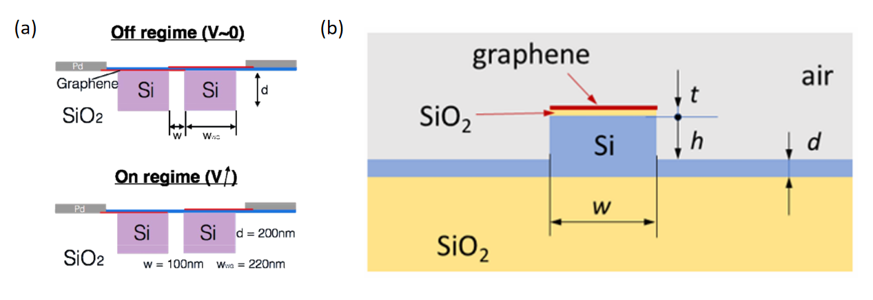
Taking advantage of this structural characteristic, Renjie Li et al. embedded an oxide layer in the lower half of the slot waveguide in 2023 and introduced a single-layer graphene in the junction region (Figure 2(b)). By regulating the chemical potential of the graphene through the gate voltage, the device simultaneously possesses phase modulation and absorption modulation functions, achieving a length of 50µm. It can perform depth modulation of 26.38dB, and the insertion loss is only 0.60Db [10]. In addition, the energy consumption in the electrical absorption and electrical refraction modulation modes is 0.51pJ/bit and 1.92pJ/bit, respectively [10]. This enables the device to simultaneously achieve high modulation efficiency, low loss, and low power consumption, providing a new idea for the research and development of high-performance optical communication network equipment.
3.2. Free-space type
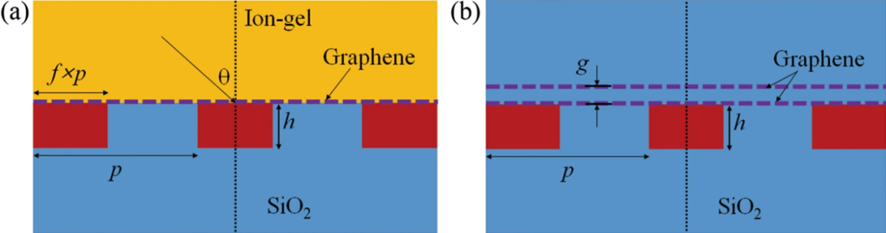
The interaction between graphene and light is relatively low, making it difficult for traditional devices to achieve high depth modulation and low insertion loss. Therefore, the free-space modulator abandons the waveguide constraint and utilizes an open system of interaction between light and matter. It enables the light beam to directly complete phase modulation at the interface between air and graphite. By constructing a vertical stack of "metal mirror - gate medium - graphene - ion gel", the incident light passes perpendicularly through the graphene plane. With the reflection enhancement of the metal mirror and the regulation of the gate electric field, realize reflective modulation [11]. In 2022, Kim M et al. designed two free-space modulators, which are single-layer graphene (SLG) + ion-gel top gate (Figure 3(a)) and double-layer graphene (DLG) + sandwich insulating layer (Figure 3(b)) [11]. Both structures are directly deposited on the surface of (Si/SiO2) one-dimensional photonic crystals. The process is simple and compatible with CMOS. Meanwhile, the mobility requirement for graphene is lenient, with µ>=0.5m2/Vs, which can maintain excellent performance [11]. This design not only breaks free from the constraints of traditional waveguide architectures but also provides new research ideas for applications such as free-space optical interconnection, laser radar and reconstructed imaging.
3.3. Fiber end face type
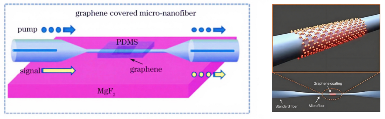
Optical fiber end-face type graphene modulators have become an important direction in all-optical modulation research in recent years due to their advantages, such as compact structure, easy integration, and fast response speed. The structure of this type of device is shown in Figure 4(a). It usually involves aligning the end faces of two standard single-mode optical fibers, with a graphene film inserted in between. By precisely controlling the position and action area of the graphene in the optical path, efficient modulation of the optical signal is achieved [12]. In 2020, Ruan Z et al. proposed a method in which the end faces of two standard single-mode optical fibers were aligned and inserted into a graphene film. One of the ends was longitudinally opened with a 1.59mm micro-slot, placing the graphene layer at the strongest point of the light field [13]. Then, together with another untreated optical fiber, they form a Mach-Zehnder interferometer as shown in Figure 4(b). The core advantage of this structure lies in the fact that it does not require electrode drive and relies entirely on optical pumping to modulate the signal light, thus featuring an extremely high response speed and low energy consumption [12]. In addition, as the device length is only at the millimeter level, it can be directly embedded in existing optical fiber links. Experiments have verified that its insertion loss is less than 1 dB and the extinction ratio reaches 20 dB, demonstrating good compatibility with existing optical communication systems [12]. This "plug and play" feature makes it have broad prospects in applications such as high-speed optical communication, optical signal processing, and optical fiber sensing.
4. Challenges and prospects
Although graphene has demonstrated unprecedented performance advantages in the field of optical communication modulators, such as ultra-wide bandwidth, low drive voltage, high-speed response, and good CMOS compatibility, it still faces a series of key challenges in the process of moving towards practical engineering and large-scale application, mainly concentrated in the following three aspects.
4.1. Regarding environmental stability issues
Graphene is prone to slow oxidation reactions in the air, especially in humid or high-temperature environments, where its sp2 hybridized structure is easily damaged. Oxidation reactions can lead to a continuous decline in carrier mobility and light absorption coefficient, thereby gradually degrading modulation efficiency and response speed. If the issue of environmental stability cannot be resolved, Graphene modulators will find it difficult to pass the reliability tests of communication equipment. Even if they demonstrate advantages such as ultra-wideband and low power consumption in the laboratory, they still cannot meet the long-term stable operation requirements of optical communication systems [14]. Therefore, it is necessary to introduce other substances or take some measures to slow down this oxidation process. Although a variety of feasible measures have been implemented nowadays, such as covering with metal oxides, introducing hydrophobic molecular buffer layers, and using nitrogen doping, there is still no single solution that can simultaneously meet the four major indicators of wafer-level uniformity, CMOS thermal budget compatibility, the lifespan of over 10 years, and zero doping and zero stress. Therefore, in the future, more in-depth research is still needed in this field to achieve more ideal antioxidant schemes, thereby promoting their large-scale industrialization.
4.2. Material transfer issues
The technical bottlenecks in the material transfer process are equally prominent. At present, the manufacturing of most graphene/silicon hybrid devices still relies on laboratory-level "wet transfer" technology, which involves transferring graphene grown by chemical vapor deposition (CVD) from copper substrates to silicon photonic chips. This method has problems such as contamination, wrinkles, and damage, and it is difficult to ensure wafer-level consistency [15]. Therefore, in the future, pollution can be reduced by developing liquid-free transfer methods (such as heat release tape, PDMS stamps, etc).
4.3. Technical bottlenecks in storage
The current mainstream packaging strategy is to use hexagonal boron nitride (h-BN) as the protective layer of graphene. By taking advantage of its atomic-level flatness, no suspension bonds, and strong chemical inertability, it can effectively prevent water and oxygen from eroding graphene, thus making it an ideal material for packaging single-layer graphene (SLG). However, due to size limitations, it is difficult to introduce it into CMOS processes [16]. In the future, a collaborative system of "material research and development - process optimization - equipment upgrading" needs to be established. By improving the h-BN preparation technology and optimizing the packaging and integration process, graphene modulators can be promoted from laboratory prototypes to industrial applications, providing core components with better performance for ultra-high-speed optical communication networks.
5. Conclusion
This paper reviews the core physical mechanisms and device development process of graphene in the field of optical communication modulators, and defines its three major working principles - the full optical threshold switching effect of saturable absorption, the refractive index change mechanism induced by strong light, and the sub-wavelength local enhancement effect of plasma coupling, which together constitute the technical cornerstone for graphene to break through the performance bottleneck of traditional devices. Among them, saturable absorption achieves ultrafast response through the Pauli blocking effect, photoinduced refractive index variation promotes device miniaturization by relying on the ultra-high third-order nonlinear polarizability, and plasma coupling achieves high modulation depth and low insertion loss by enhancing the local field strength. The synergy of the three highlights the unique advantages of graphene, such as zero band gap, ultra-high carrier mobility, and wide-spectrum response.
Meanwhile, this paper summarizes the technological breakthroughs of three typical devices since 2020: waveguide integration compresses the device length to tens of micrometers through a silicon slot structure, achieving low power consumption and compatibility with CMOS processes; The free-space type breaks free from the constraints of waveguides, providing new paths for scenarios such as optical interconnection and lidar. The optical fiber end face type achieves efficient adaptation to existing optical fiber links with its "plug and play" feature. The three have respectively made key progress in integration, application scenario expansion and system compatibility, verifying the practical potential of graphene modulators in the field of ultra-high-speed optical communication.
However, the performance degradation caused by environmental oxidation, the process defects of wet transfer, and the difficulties in the large-scale application of h-BN packaging remain the core challenges restricting its industrialization. In the future, it is necessary to promote graphene modulators from the laboratory to engineering applications by changing material properties, updating transfer technology research and development, and improving packaging processes, ultimately achieving a comprehensive performance surpassing traditional silicon-based modulators and providing core component support for the next generation of ultra-high-speed and low-power optical interconnection networks.
References
[1]. Cisco. (2020). Cisco Annual Internet Report (2018–2023) White Paper [White paper]. Cisco Systems Inc.
[2]. Reed, G. T., Mashanovich, G., Gardes, F. Y., & et al. (2010). Silicon optical modulators. Nature Photonics, 4(8), 518–526.
[3]. Bonaccorso, F., Sun, Z., Hasan, T., & et al. (2010). Graphene photonics and optoelectronics. Nature Photonics, 4(9), 611–622.
[4]. Bao, Q. L., Zhang, H., Wang, Y., & et al. (2009). Atomic-layer graphene as a saturable absorber. Advanced Functional Materials, 19(19), 3077–3083.
[5]. Hendry, E., Hale, P. J., Moger, J., & et al. (2010). Coherent nonlinear optical response of graphene. Physical Review Letters, 105(9), 097401.
[6]. Phare, C. T., Lee, Y.-H. D., Cardenas, J., & et al. (2022). Graphene electro-optic modulator with 30 GHz bandwidth. Nature Photonics, 16(7), 473–478.
[7]. Qu, S., Zhang, X., Chen, Y., & et al. (2017). Tunable graphene-based hybrid plasmonic modulators for subwavelength confinement. Scientific Reports, 7, 5190.
[8]. Kovacevic, G., Yamashita, S., Nakane, Y., & et al. (2018). Design of a high-speed graphene optical modulator on a silicon slot waveguide. Applied Physics Express, 11(6), 065102.
[9]. Petráček, J., Ctyroky, J., Kuzmiak, V., & Kwiecien, P. (2021). Coupling of waveguide mode and graphene plasmons. The European Physical Journal Conferences, 255, 07002.
[10]. Li, R. J., Yang, H., Wang, J., & et al. (2023). Semi-embedded slot waveguide electro-optic modulator. Applied Optics, 62(28), 7346–7353.
[11]. Kim, M., Kim, S., Kim, D., & et al. (2022). Graphene optical modulators using bound states in the continuum. Scientific Reports, 12(1), 1445.
[12]. Ruan, Z., Pei, L., Ning, T., & et al. (2020). All-optical fiber modulator with a graphene interlayer. Optics Communications, 463, 125917.Zhong, C., Li, J., & Lin, H. (2020). Graphene-based all-optical modulators. Frontiers of Optoelectronics, 13(2), 114–128.
[13]. Zhong, C., Li, J., & Lin, H. (2020). Graphene-based all-optical modulators. Frontiers of Optoelectronics, 13(2), 114–128.
[14]. Kawabata, S., Yamada, T., Makino, Y., & et al. (2024). Degradation of graphene in high- and low-humidity air, and vacuum conditions at 300–500 K. Nanomaterials, 14(2), 166.
[15]. Graphene on silicon photonics: Light modulation and detection for cutting-edge communication technologies. (2022). Applied Sciences, 12(1), 313.
[16]. Jin, M., Zhang, X., Wang, Y., & et al. (2022). Silicon-based graphene electro-optical modulators. Photonics, 9(2), 82.
Cite this article
Li,H. (2025). Optical Modulation Characteristics of Graphene and Its Application in Optical Communication Modulation Devices. Applied and Computational Engineering,201,1-8.
Data availability
The datasets used and/or analyzed during the current study will be available from the authors upon reasonable request.
Disclaimer/Publisher's Note
The statements, opinions and data contained in all publications are solely those of the individual author(s) and contributor(s) and not of EWA Publishing and/or the editor(s). EWA Publishing and/or the editor(s) disclaim responsibility for any injury to people or property resulting from any ideas, methods, instructions or products referred to in the content.
About volume
Volume title: Proceedings of CONF-FMCE 2025 Symposium: Semantic Communication for Media Compression and Transmission
© 2024 by the author(s). Licensee EWA Publishing, Oxford, UK. This article is an open access article distributed under the terms and
conditions of the Creative Commons Attribution (CC BY) license. Authors who
publish this series agree to the following terms:
1. Authors retain copyright and grant the series right of first publication with the work simultaneously licensed under a Creative Commons
Attribution License that allows others to share the work with an acknowledgment of the work's authorship and initial publication in this
series.
2. Authors are able to enter into separate, additional contractual arrangements for the non-exclusive distribution of the series's published
version of the work (e.g., post it to an institutional repository or publish it in a book), with an acknowledgment of its initial
publication in this series.
3. Authors are permitted and encouraged to post their work online (e.g., in institutional repositories or on their website) prior to and
during the submission process, as it can lead to productive exchanges, as well as earlier and greater citation of published work (See
Open access policy for details).
References
[1]. Cisco. (2020). Cisco Annual Internet Report (2018–2023) White Paper [White paper]. Cisco Systems Inc.
[2]. Reed, G. T., Mashanovich, G., Gardes, F. Y., & et al. (2010). Silicon optical modulators. Nature Photonics, 4(8), 518–526.
[3]. Bonaccorso, F., Sun, Z., Hasan, T., & et al. (2010). Graphene photonics and optoelectronics. Nature Photonics, 4(9), 611–622.
[4]. Bao, Q. L., Zhang, H., Wang, Y., & et al. (2009). Atomic-layer graphene as a saturable absorber. Advanced Functional Materials, 19(19), 3077–3083.
[5]. Hendry, E., Hale, P. J., Moger, J., & et al. (2010). Coherent nonlinear optical response of graphene. Physical Review Letters, 105(9), 097401.
[6]. Phare, C. T., Lee, Y.-H. D., Cardenas, J., & et al. (2022). Graphene electro-optic modulator with 30 GHz bandwidth. Nature Photonics, 16(7), 473–478.
[7]. Qu, S., Zhang, X., Chen, Y., & et al. (2017). Tunable graphene-based hybrid plasmonic modulators for subwavelength confinement. Scientific Reports, 7, 5190.
[8]. Kovacevic, G., Yamashita, S., Nakane, Y., & et al. (2018). Design of a high-speed graphene optical modulator on a silicon slot waveguide. Applied Physics Express, 11(6), 065102.
[9]. Petráček, J., Ctyroky, J., Kuzmiak, V., & Kwiecien, P. (2021). Coupling of waveguide mode and graphene plasmons. The European Physical Journal Conferences, 255, 07002.
[10]. Li, R. J., Yang, H., Wang, J., & et al. (2023). Semi-embedded slot waveguide electro-optic modulator. Applied Optics, 62(28), 7346–7353.
[11]. Kim, M., Kim, S., Kim, D., & et al. (2022). Graphene optical modulators using bound states in the continuum. Scientific Reports, 12(1), 1445.
[12]. Ruan, Z., Pei, L., Ning, T., & et al. (2020). All-optical fiber modulator with a graphene interlayer. Optics Communications, 463, 125917.Zhong, C., Li, J., & Lin, H. (2020). Graphene-based all-optical modulators. Frontiers of Optoelectronics, 13(2), 114–128.
[13]. Zhong, C., Li, J., & Lin, H. (2020). Graphene-based all-optical modulators. Frontiers of Optoelectronics, 13(2), 114–128.
[14]. Kawabata, S., Yamada, T., Makino, Y., & et al. (2024). Degradation of graphene in high- and low-humidity air, and vacuum conditions at 300–500 K. Nanomaterials, 14(2), 166.
[15]. Graphene on silicon photonics: Light modulation and detection for cutting-edge communication technologies. (2022). Applied Sciences, 12(1), 313.
[16]. Jin, M., Zhang, X., Wang, Y., & et al. (2022). Silicon-based graphene electro-optical modulators. Photonics, 9(2), 82.