


1. Introduction
With the continuous development of social production, the grid is becoming more diverse in terms of the equipment used by customers and the demand for electricity is increasing day by day. In the traditional power system, fossil fuels such as coal and gas dominate the power generation industry due to their stability and reliability [1]. However, conventional energy resources have limited quantity. In that case, people are actively seeking a comprehensive, coordinated and sustainable production mode. Under the “Carbon Neutrality” target, as an inexhaustible renewable energy source for mankind, solar power has become popular. Besides, with the significant characteristics of cleanliness, safety and universality, photovoltaic (PV) power generation plays an important role in the long-term energy strategy.
The solar photovoltaic system consists of several sub-systems, including the PV generation module, the inverter module, and the filter module. In some large-scale PV systems, an energy storage module also be equipped. These sub-systems cooperate with each other to help the PV system convert solar energy to electricity required by consumers [2]. As one of the classical converters from the power electronics devices family, the photovoltaic inverter has been applied extensively [3]. The PV inverter is an irreplaceable interface between the panel and the grid. It takes the responsibility of converting the DC voltage generated by the PV Panel to municipal frequency AC voltage. As shown in Figure 1, depending on whether equipped with a transformer, typical PV systems can be divided into isolated PV inverters and non-isolated PV inverters. Among the isolated group, the equipped transformer can work at power frequencies or high frequencies. The non-isolated inverter is also called tranformerless inverter.
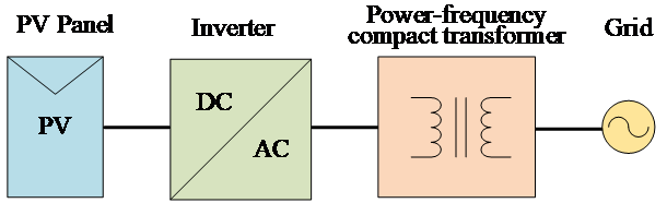
(a)
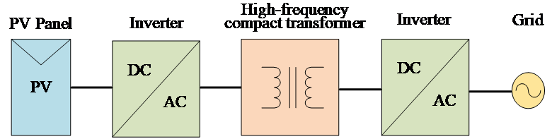
(b)
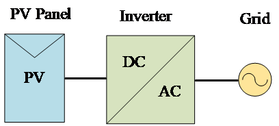
(c)
Figure 1. Different configurations of grid-connected PV systems. (a) Isolated PV system with power-frequency compact transformer. (b) Isolated PV system with high-frequency compact transformer. (c) Non-isolated PV system.
In the conventional PV system, a power-frequency compact transformer or a high-frequency compact transformer is capable to provide galvanic isolation. It effectively reduces the DC components in the system and improves the safety of operators. On the other hand, a power-frequency compact transformer has a large volume and heavy quality, which leads to a high cost. A high-frequency compact transformer increases the complexity of control, which results in additional losses and lower working efficiency. In order to overcome these weaknesses, it makes sense to go on further research on non-isolated inverters.
Non-isolated inverters have smaller volumes compared with isolated inverters. When the transformer is removed, the system’s productivity has dramatically increased. Specifically, the efficiency of the whole PV system can reach its peak at over 97%. This statistic is attractive. In contrast, due to the absence of a transformer, the galvanic connection between the PV panel and the utility grid causes a serious common-mode current problem which appears at the parasitic-capacitor between the PV negative plate and the ground [4]. The common-mode current is known colloquially as leakage current. It might cause current distortion on the grid and severe electromagnetic interference, which might reduce the sensitivity of the system [5]. Even worse, the leakage current may pollute the environment and endanger the safety of operators. Based upon that, there is a need to research the leakage current mitigation methods for transformerless PV inverters.
The scope of this paper is to provide a comprehensive overview focused on leakage current mitigation technologies for non-isolated photovoltaic inverters. In Section 2, the author will introduce the mechanism of leakage current. Based on a single-phase H-Bridge topology, the author represents the expressions of common-mode voltage and leakage current. In Section 3, the author provides various mitigation topologies and makes comparisons according to their characteristics.
2. Analysis of leakage current mechanism
2.1. Leakage current generation principle
In the PV generation module, equipment is grounded to improve the safety of operators and the PV system. The most common strategy is connecting all exposed mental devices together and making them link to the earth by an insulated frame. If there is a breakdown in the PV system, the external shell of the device will be conducted. With the help of the grounding protection strategy, the potential difference between the mental shell and the earth is mitigated to zero. In that case, it availably reduces the risk of electric shock [6]. Furthermore, the PV modules are large and flat structures. Hence, there is a parasitic capacitance existed between the PV panel and the earth. The PV panel, the capacitance, the filter, and the inverter together with network impedances consist of a common-mode resonant circuit [7]. When the PV inverter turns on or off, there will be voltage changes on the parasitic capacitor. In the common-mode resonant circuit, the changing common-mode voltage is the cause of the common-mode current, also called the leakage current. A schematic diagram of leakage current generation in a typical non-isolated PV system is illustrated in Figure 2.
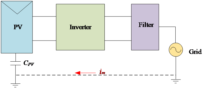
Figure 2. The generation principle of leakage current in the non-isolated PV system.
2.2. Analysis of common-mode voltage and leakage current in a typical inverter circuit
According to the different types of power supply on the DC side, PV inverters can be classified into two groups. When the power supply is a voltage source, inverters are Voltage Source Inverters (VSIs). When the supply is a current source, inverters are called Current Source Inverters (CSIs).
Both VSIs and CSIs have their unique advantages. But when taking the cost and topology principles into consideration, inverters with voltage sources are more popular among engineers. Moreover, owing that the single-phase fully-bridge inverter circuit is the most classic PV inverter topology, analysis of common-mode voltage and current will base on a single-phase fully-bridge topology.
Figure 3 below illustrates the topology of a single-phase fully-bridge inverter. The input of the inverter circuit is connected to the PV panel while the output of it links with the utility grid. The PV panel converts solar energy to DC electricity and transfers electric energy to the inverter.
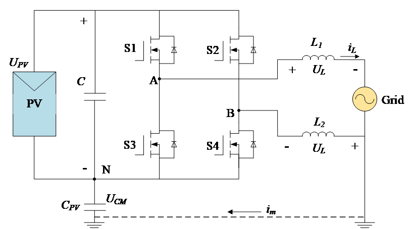
Figure 3. A single-phase fully-bridge photovoltaic inverter.
The definitions of devices set for the inverter are as followed. UPV is the output voltage of the photovoltaic array, additionally, is the input voltage of the inverter. C is a capacitor. It is connected in parallel on the DC side of the inverter circuit. S1, S2, S3, S4 are switches. L1, L2 are filter inductances. CPV is the parasitic capacitance between the PV panel and the ground. UCM, Im is the common-mode voltage and the common-mode current of the inverter respectively. The AC side of the circuit connects to the utility grid.
According to the definition of common-mode voltage and differential-mode voltage:
\( {U_{CM}}=\frac{{U_{AN}}+{U_{BN}}}{2} \) | (1) | |
\( {U_{DM}}={U_{AN}}-{U_{BN}} \) | (2) |
Specifically, UAN and UBN are the voltage from the two bridge arms to the neutral point N. UDM is the differential-mode voltage. After some conversion, the expressions for UAN and UBN are as followed.
\( {U_{AN}}={U_{CM}}+\frac{{U_{DM}}}{2} \) | (3) | |
\( {U_{BN}}={U_{CM}}-\frac{{U_{DM}}}{2} \) | (4) |
According to equations (3) and (4), it’s available to get an equivalent circuit, as shown in Figure 4.
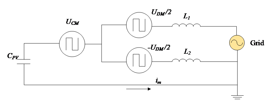
Figure 4. The equivalent circuit.
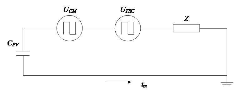
Figure 5. The most simplified circuit.
Then, it’s easy to get the most simplified circuit, as shown in Figure 5, and can be expressed as
\( {U_{TCM}}={U_{CM}}+{U_{d-c}} \) | (5) |
Ud-c represents the effect of differential-mode voltage on common mode voltage. UTCM is the total common-mode voltage in the inverter.
Owing that two filter inductors are connected in parallel, the expression of the equivalent impedance Z is
\( Z=\frac{{L_{1}}+{L_{2}}}{{L_{1}}{L_{2}}} \) | (6) |
After calculation, UTCM can be expressed as [8]
\( {U_{TCM}}=\frac{{U_{AN}}+{U_{BN}}}{2}+\frac{{L_{2}}-{L_{1}}}{2{(L_{1}}+{L_{2}})}{(U_{AN}}-{U_{BN}})-\frac{{L_{1}}}{{L_{1}}+{L_{2}}}{U_{AC}} \) | (7) |
The leakage current is mainly caused by UAN and UBN. There is negligible effect of UAC on leakage current. The expression of UTCM can be simplified as
\( {U_{TCM}}=\frac{{U_{AN}}+{U_{BN}}}{2}+\frac{{L_{2}}-{L_{1}}}{2{(L_{1}}+{L_{2}})}{(U_{AN}}-{U_{BN}}) \) | (8) |
Thus, the expression of leakage current is
\( {i_{m}}={C_{m}}\frac{d{U_{TCM}}}{dt} \) | (9) |
The magnitude of the leakage current in a non-isolated inverter is related to the parasitic capacitance UPV and the change of the total mode voltage. It’s difficult to control the parameter of UPV [9]. Hence, it’s accessible to limit the value of UTCM to zero in order to mitigate the leakage current.
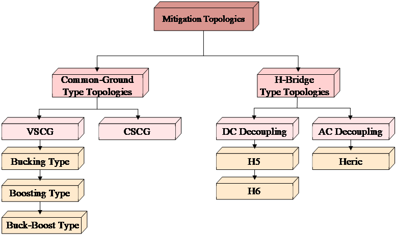
Figure 6. The classification of leakage current mitigation topologies.
3. The leakage current mitigation strategies
3.1. The classification of leakage current mitigation topologies
Currently, researches on non-isolated PV inverters are focused on two main areas. One is to improve the working efficiency of inverters while the other is to control the leakage current. Hence, numerous non-isolated PV inverter topologies have been proposed and have made significant improvements in leakage current mitigation methods. The root principle of these topologies is adding auxiliary devices to improve the original AC and DC bypasses. Compared with the conventional topology, those improved inverters have made noticeable progress in terms of the output power, harmonic distortion, DC-side midpoint potential balance and leakage current amplitude.
For non-isolated PV inverters, there are two types of topologies widely used for suppressing the leakage current. The most commonly used topologies are called Common-Ground topology and H-Bridge topology. Based on the decoupling technology, scientists have made certain improvements to the DC-side and AC-side of the inverter topology respectively. Accordingly, the H5, the H6, the Heric topology are created. In this section, the author will analyse some typical topologies and make comparison among them. Figure 6 shows a comprehensive classification of leakage current mitigation topologies.
(a)
(b)
(c)
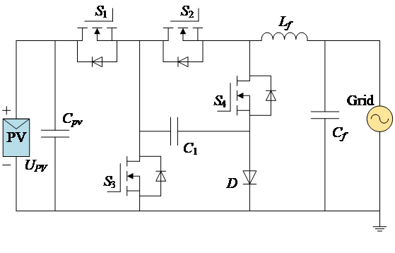
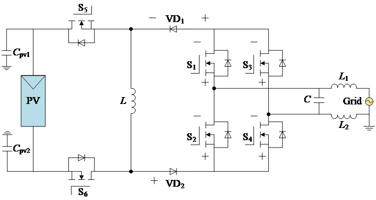
Figure 7. Typical Boosting-type inverters. (a) Topology with high boosting gain. (b) Topology with a coupled inductor. (c) Topology with five-level output signal.
3.2. The analysis of leakage current mitigation topologies
3.2.1. Common-Ground topologies. For Common-Ground topologies, the negative terminal of the photovoltaic cell is connected directly to the grid while the connection point is connected to the earth. With such characteristic, the inverter is vividly named Common-Ground (CG) inverter.
The CG PV inverters can be divided into two categories: voltage-source common-ground topology (VSCG) and current-source common-ground topology (CSCG). Among the VSCG category, there are Boosting-type topologies, Bucking-type topologies and Buck-Boost-type topologies.
The main characteristic of the CG inverter is that the negative terminal of the PV cell is connected directly to the grid neutral line and the junction is linked to the ground. Thus, the parasitic capacitance is completely shorted, and the common-mode voltage is constant. In Consequence, Common-Ground topologies are able to eliminate the leakage current completely. But every topology has its advantages and disadvantages. The author will introduce the VSCG and the CSCG in detail.
(1). VSCG
The VSCG PV inverters are widely applied in practical engineering projects due to their high efficiency and low cost. In order to solve the leakage current issue, Boosting-type topologies, Bucking type topologies and Buck-Boost type topologies all make contributions.
(i). Boosting-type topologies
For Boosting type topologies, there are fewer decoupling capacitors designed in the circuit. Thus, it effectively increases the reliability of the system operation. Additionally, Boosting-type topologies require continuous input current which makes it easier for analyzing the Maximum Power Point Tracking (MPPT).
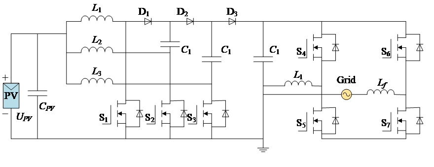
Figure 7 illustrates some typical Boosting-type topologies. Detailed analysis will be served in the paper.
For Type A-Boosting topology, as shown in Figure 7(a), a large number of switching capacitors are added to the circuit. This design provides significant boost gain, which helps the inverter cooperates with the utility grid better. Besides, this topology requires numerous semiconductor devices. The parameters for these devices are small to restrict negative impacts on the circuit. However, the complexity of the circuit is significantly increased so more advanced manufacturing techniques and more production costs are required.
For the Type B-Boosting topology in Figure 7(b), in order to improve the boosting gain, the designers add a coupled inductor in the circuit. However, it can’t be ignored that the participation of the coupled inductor makes the circuit more complex. In that case, the cost of the inverter will more expensive. Also, there is the problem of high voltage stress of switches, which may decrease the working efficiency.
For Type C-Boosting illustrated in Figure 7(c), it provides a five-level voltage output to raise the operating efficiency. In order to control the output signal, the circuit requires more switches. Besides, to make the output voltage more accurate, additional electrolytic capacitors are needed to balance the voltage drop across the capacitors. Although the capacitance devices are not need to be recharged, the circuit is much complexed than others.
(ii). Bucking-type topologies
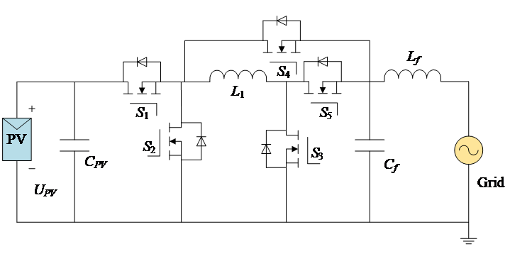
Type A-Bucking topology shown in Figure 8(a) shows the most classic Bucking structure.
Compared with the Boosting inverters, the majority of Bucking inverters have discontinuous input current. To solve the problem caused by discontinuous current, an additional DC-DC converter connected to the PV panel is achievable. Type B-Bucking topology in Figure 8(b) is a good example. Such improvement, on the one hand, helps the MPPT analysis more effective. On the other hand, it reduces the economic benefit and operation efficiency of the inverter.
Commonly, the Bucking inverters output a three-level voltage signal. Some special topologies are able to output voltage of different levels. For example, the Type B-Bucking inverter outputs a two-level voltage signal, while the Type C-Bucking inverter in Figure 8(c) has a five-level voltage output. In general, the less the voltage level that a Bucking-type inverter outputs, the larger the filter is required in the PV system. Accordingly, it’s accessible to improve the economic performance of a Bucking inverter from this aspect.
(a)
(b)
(c)
Figure 8. Different structures of Bucking-type inverters. (a) The basic Bucking inverter. (b) Bucking topology with continuous current. (c) Bucking inverter with two-level output signal.
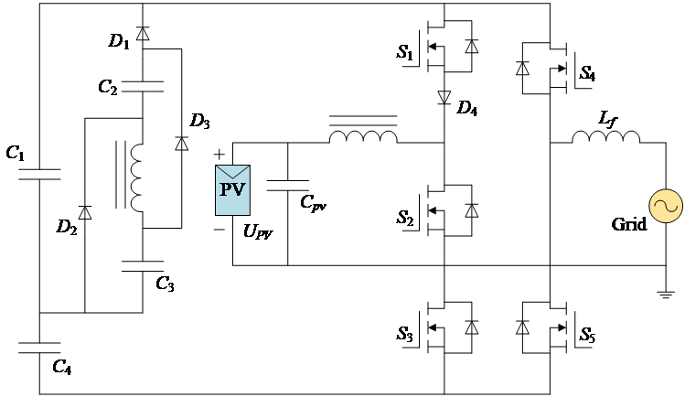
(iii). Buck-Boost-type topologies
Bucking-type topologies and Boosting-type topologies can only realize the bucking or boosting function. Photovoltaic cells easily generate voltage with unbearable fluctuation due to the surrounding influence. Hence, an adequate adjustment range is needed for controlling the output signal. In that case, owing to the flexible boosting and bucking capability, Buck-Boost-type inverters are of significant researching importance. In addition to the basic leakage current mitigation function, Buck-Boost inverters can withstand different voltage levels. They help PV systems more suitable for utility grid operation. Thus, Buck-Boost type inverters have a wide range of applications.
Buck-Boost inverters combine the advantages of Bucking topologies and Boosting topologies. Some structures of Buck-Boost inverters are presented in Figure 9.
(a)
(b)
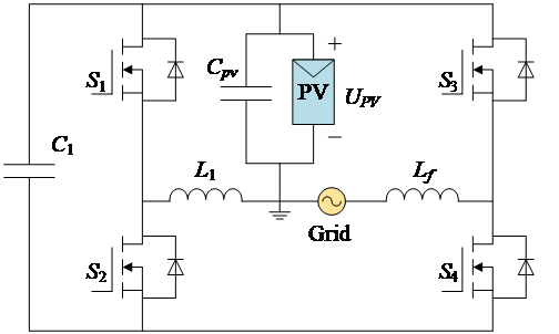
Figure 9. Buck-Boost-type inverters. (a) Topology proposed in [10]. (b) Topology proposed in [5].
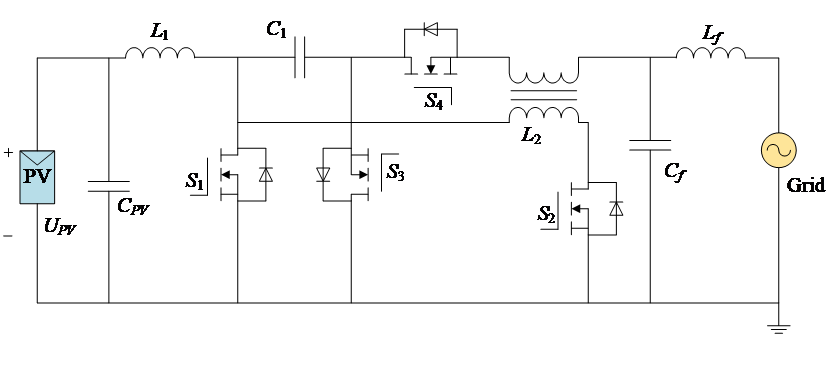
For Type A-Buck-Boost topology as shown in Figure 9(a), the circuit consists of three main sections. The output terminal of the PV panel is connected to a Boosting-type MPPT circuit. The IGBT S1 and S3, the inductor L2, together with the capacitor C2 makes of a bidirectional Buck-Boost circuit. Meanwhile, S2, S4 and inductor L3 consist of a half-bridge inverter circuit. Specifically, the bidirectional Buck-Boost circuit is served to balance the voltage between capacitors C1 and C2. The half-bridge inverter circuit is designed to control grid current.
Besides, electrolytic capacitors or large inductors are not required in this topology. There are few devices in the circuit, thus, it greatly improves the economic performance and operability of the inverter. Additionally, this topology enables a step-up inversion, which reduces the ripple of the pre-stage output voltage. It’s noticeable that the leakage current in this topology is completely controlled to zero and the PV system is allowed to operate efficiently and stably. However, one of the limitations of this topology is that only the leakage current generated on the negative terminal of the PV panel is taken into account.
Type B-Buck-Boost topology shown in Figure 9(b) has made improvements based on the basic structure.
Type B-Buck-Boost inverter has a symmetrical structure and it takes into account the leakage current generated in the positive and negative plates of the PV panel. Meanwhile, this circuit represents a Single-phase single-stage Buck-Boost inverter, which can be controlled by the modulation ratio to achieve a balanced lift-off conversion. It’s noticeable that there are no electrolytic capacitors required in Type B-Buck-Boost topology. Thus, compared with multistage inverters, this topology has simpler circuit structure and better system efficiency.
(2). CSCG
CSCG type inverters use inductors as energy storage elements. However, these inductors will lead to problems of larger inverter size, higher cost and lower power density of inverter.
Figure 10 below shows some CSCG topologies.
(a)
(b)
Figure 10. CSCG inverters. (a) Topology proposed in [11]. (b) Topology proposed in [12].
There are five switching tubes to control the ON and OFF state of Type A-CSCG topology which is presented in Figure 10(a). When the circuit is working at high frequencies, S2, S4 and S5 will turn on while S1 switches on at low frequencies. When the input voltage is negative, S3 starts to operate. The circuit is designed with two inductors. L1 serves to amplify the voltage across the distribution capacitor CPV and to transmit voltage to the utility grid. Lf and Cf make up a filter circuit, which might contribute to reduce grid harmonics.
The five switching tubes are not connected in parallel with the freewheeling diodes. This design is available to reduce the number of devices and reduce the switching loss. Also, this topology requires a discontinuous input current. In that case, it’s difficult for MPPT analysis. Besides, all switches are unidirectionally conducted. It reduces the cost of the circuit but restricting switches working with unity power factor.
For Type B-CSCG topology in Figure 10(b), the circuit components and structure are similar to the other CG topologies. Compared with the Type A-CSCG inverter, it adds a freewheeling diode to output a continuous current which makes the circuit easier to be analysed. Also, the designer adds an electromagnetic coupling section. In this section, there is a double-winding coupling inductor which is beneficial to maintain current continuity. However, it may increase the manufacturing cost and decrease the working efficiency of the inverter to some degree.
3.2.2. H-Bridge topologies. Full-bridge inverters, also known as H-Bridge inverters or H4 inverters. With the advantages of high output voltage quality, high power conversion efficiency and small sizes, H-Bridge inverters are popular in photovoltaic systems.
For H-Bridge inverters, there are generally two modulation methods: unipolar modulation and bipolar modulation. However, the analysis above shows that there is severe leakage current problem for H-Bridge inverters when using the unipolar modulation method. When bipolar modulation is used, the leakage current issue is solved but the switching loss of the circuit is higher due to more IGBTs being added to the topology. Also, the output voltage is bipolar owing that it’s influenced by the modulating signal. In that case, there will be a larger ripple in output voltage and current, which affects the operational efficiency of inverters. Hence, conventional H-Bridge inverters are not the best choice in photovoltaic systems.
For H-Bridge inverters with DC bypass, the most typical topologies are the H5 inverter proposed by SMA in Germany and the H6 inverter proposed by Ingeteam. A typical AC bypass inverter is the Heric inverter proposed by Sunways. The following section will analyse and compare these inverters in detail.
(1). H5 inverter
Based on the conventional H-Bridge topology, the H5 inverter adds a power switch to the DC side. This improved design separates the freewheeling circuit from the power supply. In that case, the common-mode voltage remains constant and achieves the purpose of mitigating leakage current.
This topology was proposed and patented by the company SMA. Grid-connected inverters from the Sunny Mini Central series of SMA using this H5 topology. Also, it’s claimed that the efficiency of this H5 inverter reaches its peak at 98.1%.
Figure 11 below presented the H5 inverter.
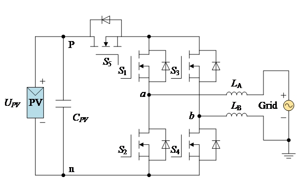
Figure 11. H5 inverter.
There are five IGBTs designed in the H5 inverter topology. Among them, S1 and S3 alternately turn on at the positive and negative half wave of the input voltage. The role of S5 is to modulate the frequency. During one voltage cycle, the common-mode voltage always remains the value of 0.5UPV. Hence, as long as the output voltage of PV cells is kept constant, the common-mode voltage can be kept constant, so as to prevent leakage current.
Compared with other topologies, the H5 inverter has a simpler circuit structure and fewer circuit components, which make it highly economical in photovoltaic projects. However, as S5 always operates at high frequencies, the heat loss on it is more than other switches. Thus, the loss imbalance issue isn’t be ignored in the H5 topology.
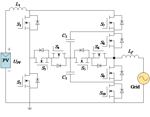
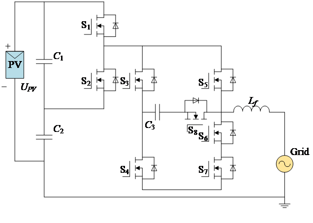
(2). H6 inverter
Based on the single-phase fully-bridge inverter, the H6 inverter adds two power switches and diodes on the DC-rail. Additionally, two clamping diodes are set anti-parallel next to the switches to achieve the current commutation and continuation.
There are various H6 topologies for application. Figure 12 shows the most typical one.
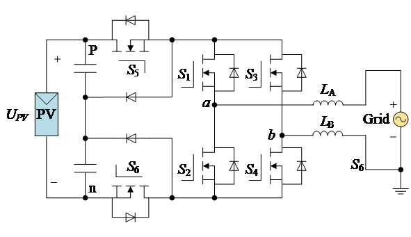
Figure 12. H6 inverter topology.
In this H6 topology, there are six switches, of which S5 and S6 operate at high frequencies and the remaining four switches work at power frequency. S1 and S4 are modulated by the same unipolar PWM signal while S2 and S3 are controlled by the other. The two sets of signals are complementary. The common-mode voltage is constantly equal to 0.5UPV and thus inhibits leakage current in the inverter.
Compared with conventional H-Bridge inverter, the H6 inverter has fewer switches working at high frequencies. This results in lower switching losses and higher operational efficiency. If fast recovery diodes (FRD) are used to replace the normal diodes, switching losses in the inverter can be significantly reduced.
(3). Heric inverter
The full name of the Heric inverter is Highly Efficient and Reliable Inverter Concept. This is the topology developed by Sunway.
The Heric inverter topology is shown as followed.
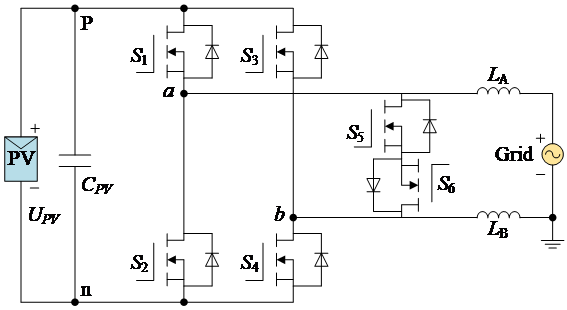
Figure 13. Heric inverter topology.
Compared with the conventional one, the structural characteristic of Heric inverter is that two power switches in opposite directions are added between the Busbar of AC bypass. In that case, this design allows for a bidirectional freewheeling circuit which helps the PV battery decouple from the grid and limit the leakage current generation. It can’t be ignored that the potential of freewheeling circuit is too small, a varying common-mode voltage is still existed. Thus, the leakage current is not completely suppressed. Nevertheless, the Heric inverter are capable to limit the leakage current within an acceptable range. In addition, it can provide high operation efficiency so the Heric inverter are popular among electrical engineers.
3.3. The comparisons of leakage current mitigation topologies
In light of the analysis above, the author makes a table to make objective comparisons.
According to the characteristics of each topology, the author will make comparisons in terms of the ability of leakage current mitigation, the circuit structure and the economic performance of the inverter.
Table 1. Comparisons of Common-Ground type topologies.
Type | Classifications | Advantages | Limitations |
VSCG | Type A-Boosting Topology | • Completely mitigate leakage current • High boosting gain. | • More devices needed • Complex structure |
Type B-Boosting Topology | • Completely mitigate leakage current • Coupled inductor enhances boosting capability. | • The coupled inductor makes the inverter larger and less efficient. | |
Type C-Boosting Topology | • Completely mitigate leakage current • Five-level output voltage. | • More switches needed • Additional electrolytic capacitor needed • Complex topology structure | |
Type A-Bucking Topology | • Completely mitigate leakage current. | • Discontinuous input current • Difficult for MPPT | |
Type B-Bucking Topology | • Completely mitigate leakage current • Continuous input current; • Two-level output voltage. | • Large filter size. | |
Type C-Bucking Topology | • Completely mitigate leakage current; Five-level output voltage. | • Discontinuous input current • Increased circuit complexity. | |
Type A-Buck-Boost Topology | • Flexible boosting and bucking • Completely mitigate leakage current • No need for high-capacity inductors • Reduced ripple in the output voltage. | • Only consider leakage current of the negative PV terminal. | |
Type B-Buck-Boost Topology | • Completely mitigate leakage current • No need for electrolytic capacitors • Symmetric structure. | —— | |
Table 1. (continued). | |||
CSCG | Type A-CSCG Topology | • Completely mitigate leakage current • Unidirectionally conducted switches • Lower cost | • Discontinuous input current; Switches only work with unity power factor • Inflexible operation performance. |
Type B-CSCG Topology | • Completely mitigate leakage current • Coupled inductor helps for continuous current | • Coupled inductor increases the cost and reduces operational efficiency. | |
Table 2. Comparisons of H-Bridge type topologies.
Type | Classifications | Advantages | Limitations |
DC Decoupling | H5 | • Simple structure • Need for fewer devices | • Leakage current still existed • Imbalanced loss |
H6 | • Low switching loss • Balance heat loss • Simple circuit with lower cost | • Leakage current cannot be completely suppressed. | |
AC Decoupling | Heric | • Symmetrical structure • High working efficiency • Leakage current can be limited within a range | • Leakage current cannot be completely suppressed. |
3.4. Improvements for leakage current mitigation topologies
As an important technology for renewable energy generation, the development of non-isolated photovoltaic inverters is becoming increasingly mature. All electrical engineers are looking forward to inverters with higher operation efficiency, simpler structures and greater reliability. Based on the analysis of the two categories of inverters above, the author makes a proposal for their future development.
For Common-Ground inverters, the most significant characteristic is that the leakage current problem can be solved completely. Accordingly, (1) Increase the output level of inverters. It not only simplifies the design of the inverter's switching devices, but also makes the filter smaller in size. The multi-level CG circuit design effectively provides improvements in terms of both operational efficiency and economic performance; (2) Combined with the magnetic integration technology. In order to raise the boosting gain, the conventional solutions are cascading, adding switching capacitors or inductors, or coupling inductors. These conventional strategies all have their own shortcomings and are not suitable for more rigorous occasions. Hence, the technique of magnetic integration can be used to reduce voltage stress on the switches while providing high boosting gain. Also, this technology is good to reduce ripple in the inductor current [13].
For H-Bridge inverters, the most significant feature is the simple topology structure. In that case, the operation performance can be strengthened in terms of improving the switching frequency of the switches. (1) Use wide bandgap materials. Conventional switching tubes use materials such as Si, Ge and C but wide bandgap materials like SiC, GaN, have higher output power, more stable physical and chemical properties. Hence, the switching losses in non-isolated PV inverters can be effectively reduced and the operating efficiency of inverters get improvements. (2) Improve controlling techniques. PWM technology is commonly used in modern circuit control. Since the utility grid requires a sinusoidal electrical signal, the SPWM technique can be used to help the inverter be controlled more precisely. Besides, to reduce harmonics in the circuit, the SHEPWM technique can be used to eliminate a specified number of harmonics. Also, the SVPWM technique provides output voltage with higher quality.
4. Conclusion
In this paper, the author provides a comprehensive overview focusing on the leakage current mitigation strategy of non-isolated photovoltaic inverters. By analysing the leakage current of a single-phase non-isolated inverter circuit, it can be seen that controlling the common-mode voltage can effectively solve the leakage current problem. Accordingly, leakage current mitigation topologies can be classified into two categories, which are Common-Ground topologies and H-Bridge topologies. These two types of topologies can be further classified. All topologies analysed in the paper significantly suppress leakage currents of non-isolated PV inverters. Also, the author makes a table to make comparisons for their characteristics. Basically, CG topologies are able to mitigate leakage current completely. In general, a CG inverter topology requires more components, such as coupling inductors, and a larger number of inductors. To some extent, this increases the losses in the circuit and affects its operational efficiency. Besides, CG topology has an asymmetrical structure and a discontinuous input current. In that case, the analysis of CG topologies is difficult. H-Bridge topologies are unable to suppress leakage currents completely due to their structures. Nevertheless, they can limit the leakage current within an acceptable range. The H-Bridge inverter requires fewer devices and has lower switching losses. Thus, this kind of topology can ensure the efficient operation of the PV inverter. At the same time, the H-Bridge inverter is smaller in size and less expensive in cost, which makes it superior in terms of economic performance. For both types of inverter topology, increasing the output voltage level, using wide bandgap materials or more advanced techniques are available to improve the efficiency. It’s foreseeable that in the near future, inverters with higher operating efficiency and better performance will be applied in PV systems.
References
[1]. Jingyuan Cui, Haibo Wang, Yaokai Liu, Yaling Liu. “The Transformation and Upgrading Path of Power Generation Enterprises under the Goal of Carbon Neutrality”. China Power Enterprise Management. 2021, 649(28), p.p. 77-78.
[2]. Zhiqiang Gao, Hanbo Chen, Xuesong Zhou, Youjie Ma. “Chaotic control of a single-phase H-bridge PV inverter”. Journal of Vibration and Shock. 2023, 42(02), p.p. 157-165+174.
[3]. Lin Ma, Kai Sun, Remus Teodorescu, Xinmin Jin. “Comparison of the Topologies of High Efficiency Neutral Point Clamping Photovoltaic Inverters”. Transactions of China Electrotechnical Society. 2011, 26(02), p.p. 108-114.
[4]. Xiaoqiang Guo, Xiaoyu Jia. “Analysis of Common Mode Leakage Current for Transformerless Cascaded H5 PV Inverter”. Transactions of China Electrotechnical Society. 2018, 33(02), p.p. 361-369.
[5]. Liqiao Wang, Jianyi Chen, Chen Wu. “A Single-Stage Single-Phase Buck-Boost Pv Inverter which can Suppress Leakage Current”. Acta Energiae Solaris Sinica. 2022, 43(11), p.p. 41-49.
[6]. Xiaoxu Yu. “Research on the Application of Solar Photovoltaic Power Generation Grid-Connected Technology”. Equipment Technology. 2020, 176(02), p.p. 183.
[7]. Tina, Giuseppe Marco, Rosa-Clot, et al. “Numerical and Experimental Analysis of Photovoltaic Cells Under a Water Layer and Natural and Artificial Light”. IEEE journal of photovoltaics. 2019, 9(03), p.p. 733-740.
[8]. Caixue Chen, Zongyuan Liu, Lucheng Zhang. “A Low Leakage Current Non-Isolated Single-Phase Photovoltaic Grid-Connected Inverter Based on HERIC Topology”. Journal Of Power Supply. 2023, p.p. 1-11.
[9]. Yang Zhang, Min Zhang, Wei Zhang. “Analysis on Leakage Current of Non-isolated Photovoltaic Grid-connected Inverter”. Electric Safety Technology. 2021, 23(03), p.p. 1-11.
[10]. Gautam Vasav, Kumar Ashok, Sensarma Parthasarathi. “A Novel Single Stage, Transformerless PV Inverter”. In IEEE International Conference on Industrial Technology, Busan, p.p. 907-912, 2014.
[11]. Tofigh Azary Mehdi, Sabahi Mehran, Babaei Ebrahim, Abbasi Aghdam Meinagh Farhad. “Modified Single-Phase Single-Stage Grid-Tied Flying Inductor Inverter with MPPT and Suppressed Leakage Current”. IEEE Transactions on Industrial Electronics. 2018, 65(01), p.p. 221-231.
[12]. Zhi Hou. “Research on a Leakage-free Non-isolated Photovoltaic Grid-connected Inverters”. Electric Engineering. 2022, 532(22), p.p. 59-62+65.
[13]. Hongzhu Li, Feiyang Liu, Yan Liu, Hongfan Li. “A New Magnetically Integrated High Gain Coupled Inductance Voltage-Doubled Boost Converter”. Transactions of China Electrotechnical Society. 2020, 35(S2), p.p. 450-460.
Cite this article
Jiang,Y. (2023). Comprehensive analysis of current mitigation strategies for non-isolated photovoltaic inverter. Applied and Computational Engineering,11,8-23.
Data availability
The datasets used and/or analyzed during the current study will be available from the authors upon reasonable request.
Disclaimer/Publisher's Note
The statements, opinions and data contained in all publications are solely those of the individual author(s) and contributor(s) and not of EWA Publishing and/or the editor(s). EWA Publishing and/or the editor(s) disclaim responsibility for any injury to people or property resulting from any ideas, methods, instructions or products referred to in the content.
About volume
Volume title: Proceedings of the 2023 International Conference on Mechatronics and Smart Systems
© 2024 by the author(s). Licensee EWA Publishing, Oxford, UK. This article is an open access article distributed under the terms and
conditions of the Creative Commons Attribution (CC BY) license. Authors who
publish this series agree to the following terms:
1. Authors retain copyright and grant the series right of first publication with the work simultaneously licensed under a Creative Commons
Attribution License that allows others to share the work with an acknowledgment of the work's authorship and initial publication in this
series.
2. Authors are able to enter into separate, additional contractual arrangements for the non-exclusive distribution of the series's published
version of the work (e.g., post it to an institutional repository or publish it in a book), with an acknowledgment of its initial
publication in this series.
3. Authors are permitted and encouraged to post their work online (e.g., in institutional repositories or on their website) prior to and
during the submission process, as it can lead to productive exchanges, as well as earlier and greater citation of published work (See
Open access policy for details).
References
[1]. Jingyuan Cui, Haibo Wang, Yaokai Liu, Yaling Liu. “The Transformation and Upgrading Path of Power Generation Enterprises under the Goal of Carbon Neutrality”. China Power Enterprise Management. 2021, 649(28), p.p. 77-78.
[2]. Zhiqiang Gao, Hanbo Chen, Xuesong Zhou, Youjie Ma. “Chaotic control of a single-phase H-bridge PV inverter”. Journal of Vibration and Shock. 2023, 42(02), p.p. 157-165+174.
[3]. Lin Ma, Kai Sun, Remus Teodorescu, Xinmin Jin. “Comparison of the Topologies of High Efficiency Neutral Point Clamping Photovoltaic Inverters”. Transactions of China Electrotechnical Society. 2011, 26(02), p.p. 108-114.
[4]. Xiaoqiang Guo, Xiaoyu Jia. “Analysis of Common Mode Leakage Current for Transformerless Cascaded H5 PV Inverter”. Transactions of China Electrotechnical Society. 2018, 33(02), p.p. 361-369.
[5]. Liqiao Wang, Jianyi Chen, Chen Wu. “A Single-Stage Single-Phase Buck-Boost Pv Inverter which can Suppress Leakage Current”. Acta Energiae Solaris Sinica. 2022, 43(11), p.p. 41-49.
[6]. Xiaoxu Yu. “Research on the Application of Solar Photovoltaic Power Generation Grid-Connected Technology”. Equipment Technology. 2020, 176(02), p.p. 183.
[7]. Tina, Giuseppe Marco, Rosa-Clot, et al. “Numerical and Experimental Analysis of Photovoltaic Cells Under a Water Layer and Natural and Artificial Light”. IEEE journal of photovoltaics. 2019, 9(03), p.p. 733-740.
[8]. Caixue Chen, Zongyuan Liu, Lucheng Zhang. “A Low Leakage Current Non-Isolated Single-Phase Photovoltaic Grid-Connected Inverter Based on HERIC Topology”. Journal Of Power Supply. 2023, p.p. 1-11.
[9]. Yang Zhang, Min Zhang, Wei Zhang. “Analysis on Leakage Current of Non-isolated Photovoltaic Grid-connected Inverter”. Electric Safety Technology. 2021, 23(03), p.p. 1-11.
[10]. Gautam Vasav, Kumar Ashok, Sensarma Parthasarathi. “A Novel Single Stage, Transformerless PV Inverter”. In IEEE International Conference on Industrial Technology, Busan, p.p. 907-912, 2014.
[11]. Tofigh Azary Mehdi, Sabahi Mehran, Babaei Ebrahim, Abbasi Aghdam Meinagh Farhad. “Modified Single-Phase Single-Stage Grid-Tied Flying Inductor Inverter with MPPT and Suppressed Leakage Current”. IEEE Transactions on Industrial Electronics. 2018, 65(01), p.p. 221-231.
[12]. Zhi Hou. “Research on a Leakage-free Non-isolated Photovoltaic Grid-connected Inverters”. Electric Engineering. 2022, 532(22), p.p. 59-62+65.
[13]. Hongzhu Li, Feiyang Liu, Yan Liu, Hongfan Li. “A New Magnetically Integrated High Gain Coupled Inductance Voltage-Doubled Boost Converter”. Transactions of China Electrotechnical Society. 2020, 35(S2), p.p. 450-460.